Äîêóìåíòàöèÿ è îïèñàíèÿ www.docs.chipfind.ru
1
Data sheet acquired from Harris Semiconductor
SCHS157
Features
· Buffered Inputs
· Typical f
MAX
= 50MHz at V
CC
= 5V, C
L
= 15pF, T
A
= 25
o
C
· Fanout (Over Temperature Range)
- Standard Outputs . . . . . . . . . . . . . . . 10 LSTTL Loads
- Bus Driver Outputs . . . . . . . . . . . . . 15 LSTTL Loads
· Wide Operating Temperature Range . . . -55
o
C to 125
o
C
· Balanced Propagation Delay and Transition Times
· Significant Power Reduction Compared to LSTTL
Logic ICs
· HC Types
- 2V to 6V Operation
- High Noise Immunity: N
IL
= 30%, N
IH
= 30% of V
CC
at V
CC
= 5V
· HCT Types
- 4.5V to 5.5V Operation
- Direct LSTTL Input Logic Compatibility,
V
IL
= 0.8V (Max), V
IH
= 2V (Min)
- CMOS Input Compatibility, I
l
1
µ
A at V
OL
, V
OH
Pinout
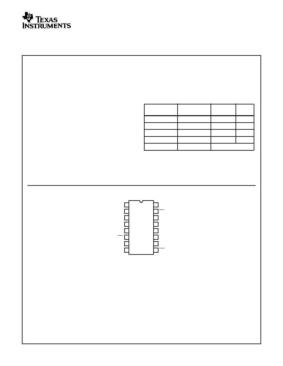
CD74HC166, CD74HCT166 (PDIP, SOIC)
TOP VIEW
Ordering Information
PART NUMBER
TEMP. RANGE
(
o
C)
PACKAGE
PKG.
NO.
CD74HC166E
-55 to 125
16 Ld PDIP
E16.3
CD74HCT166E
-55 to 125
16 Ld PDIP
E16.3
CD74HC166M
-55 to 125
16 Ld SOIC
M16.15
CD74HCT166M
-55 to 125
16 Ld SOIC
M16.15
CD54HC166W
-55 to 125
Wafer
NOTES:
1. When ordering, use the entire part number. Add the suffix 96 to
obtain the variant in the tape and reel.
2. Wafer and die is available which meets all electrical
specifications. Please contact your local sales office or Harris
customer service for ordering information.
14
15
16
9
13
12
11
10
1
2
3
4
5
7
6
8
DS
D0
D1
D2
D3
CE
GND
CP
V
CC
D7
Q7
D6
D5
D4
MR
PE
February 1998
CAUTION: These devices are sensitive to electrostatic discharge. Users should follow proper IC Handling Procedures.
Copyright
©
Harris Corporation 1998
CD74HC166,
CD74HCT166
High Speed CMOS Logic
8-Bit Parallel-In/Serial-Out Shift Register
File Number
1501.1
[ /Title
(CD74
HC166
,
CD74
HCT16
6)
/Sub-
ject
(High
Speed
CMOS
Logic
8-Bit
Paral-
lel-
In/Seri
2
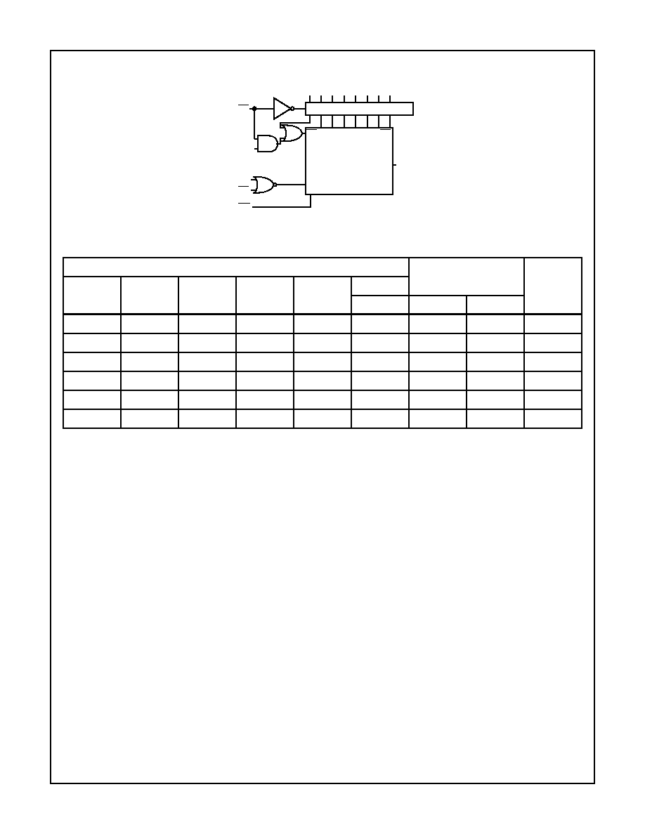
Functional Diagram
TRUTH TABLE
INPUTS
INTERNAL
Q STATES
OUTPUT
Q7
MASTER
RESET
PARALLEL
ENABLE
CLOCK
ENABLE
CLOCK
SERIAL
PARALLEL
D0 D7
Q0
Q1
L
X
X
X
X
X
L
L
L
H
X
L
L
X
X
Q00
Q10
Q0
H
L
L
X
a...h
a
b
h
H
H
L
H
X
H
Q0n
Q6n
H
H
L
L
X
L
Q0n
Q6n
H
X
H
X
X
Q00
Q10
Q70
NOTES:
H = High Voltage Level
L = Low Voltage Level
X = Don't Care
= Transition from Low to High Level
a...h = The level of steady-state input at inputs D0 thru D7, respectively.
Q00, Q10, Q70 = The level of Q0, Q1, or Q7, respectively, before the indicated steady-state input conditions were established.
Q0n, Q6n = The level of Q0 or Q6, respectively, before the most recent
transition of the clock.
8 - REGISTERS
PARALLEL ENABLE CIRCUIT
D0 D1 D2 D3 D4 D5 D6 D7
PE
D
S
CP
CE
MR
D0
D7
Q7
CD74HC166, CD74HCT166
3
Absolute Maximum Ratings
Thermal Information
DC Supply Voltage, V
CC
. . . . . . . . . . . . . . . . . . . . . . . . -0.5V to 7V
DC Input Diode Current, I
IK
For V
I
< -0.5V or V
I
> V
CC
+ 0.5V
. . . . . . . . . . . . . . . . . . . . . .±
20mA
DC Output Diode Current, I
OK
For V
O
< -0.5V or V
O
> V
CC
+ 0.5V
. . . . . . . . . . . . . . . . . . . .±
20mA
DC Drain Current, per Output, I
O
For -0.5V < V
O
< V
CC
+ 0.5V
. . . . . . . . . . . . . . . . . . . . . . . . . .±
25mA
DC Output Source or Sink Current per Output Pin, I
O
For V
O
> -0.5V or V
O
< V
CC
+ 0.5V
. . . . . . . . . . . . . . . . . . . .±
25mA
DC V
CC
or Ground Current, I
CC or
I
GND
. . . . . . . . . . . . . . . . . .±
50mA
Operating Conditions
Temperature Range (T
A
) . . . . . . . . . . . . . . . . . . . . . -55
o
C to 125
o
C
Supply Voltage Range, V
CC
HC Types . . . . . . . . . . . . . . . . . . . . . . . . . . . . . . . . . . . . .2V to 6V
HCT Types . . . . . . . . . . . . . . . . . . . . . . . . . . . . . . . . .4.5V to 5.5V
DC Input or Output Voltage, V
I
, V
O
. . . . . . . . . . . . . . . . . 0V to V
CC
Input Rise and Fall Time
2V . . . . . . . . . . . . . . . . . . . . . . . . . . . . . . . . . . . . . . 1000ns (Max)
4.5V. . . . . . . . . . . . . . . . . . . . . . . . . . . . . . . . . . . . . . 500ns (Max)
6V . . . . . . . . . . . . . . . . . . . . . . . . . . . . . . . . . . . . . . . 400ns (Max)
Thermal Resistance (Typical, Note 3)
JA
(
o
C/W)
PDIP Package . . . . . . . . . . . . . . . . . . . . . . . . . . . . .
90
SOIC Package . . . . . . . . . . . . . . . . . . . . . . . . . . . . .
160
Maximum Junction Temperature . . . . . . . . . . . . . . . . . . . . . . . 150
o
C
Maximum Storage Temperature Range . . . . . . . . . .-65
o
C to 150
o
C
Maximum Lead Temperature (Soldering 10s) . . . . . . . . . . . . . 300
o
C
(SOIC - Lead Tips Only)
CAUTION: Stresses above those listed in "Absolute Maximum Ratings" may cause permanent damage to the device. This is a stress only rating and operation
of the device at these or any other conditions above those indicated in the operational sections of this specification is not implied.
NOTE:
3.
JA
is measured with the component mounted on an evaluation PC board in free air.
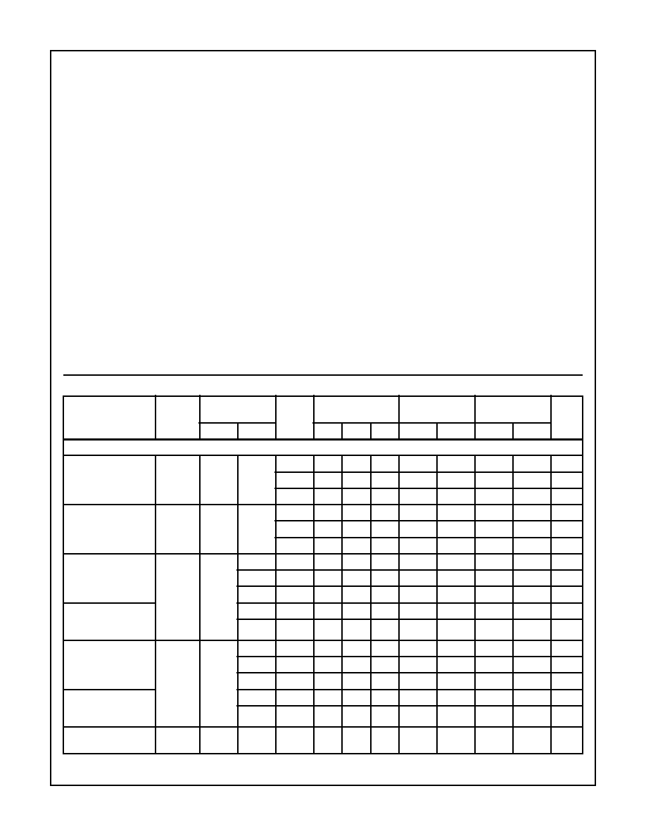
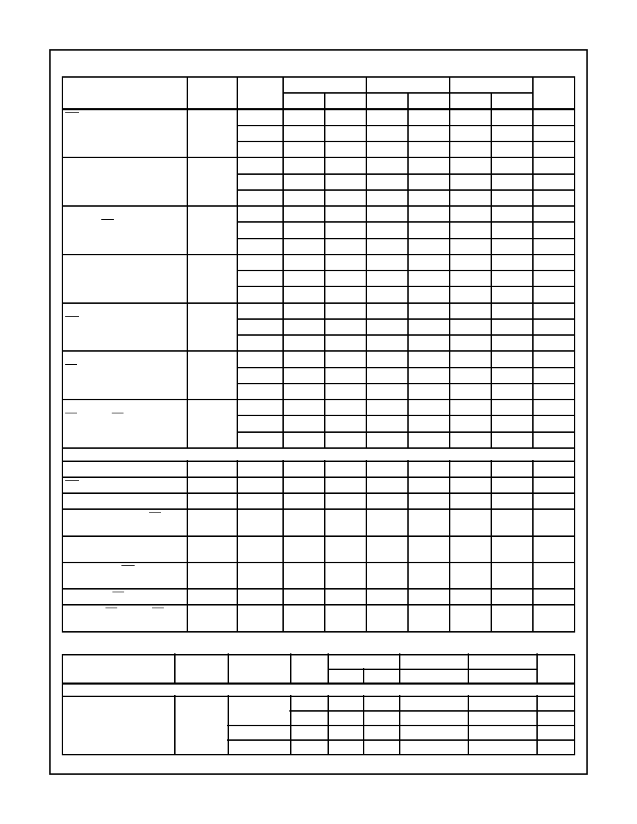
DC Electrical Specifications
PARAMETER
SYMBOL
TEST
CONDITIONS
V
CC
(V)
25
o
C
-40
o
C TO 85
o
C
-55
o
C TO 125
o
C
UNITS
V
I
(V)
I
O
(mA)
MIN
TYP
MAX
MIN
MAX
MIN
MAX
HC TYPES
High Level Input
Voltage
V
IH
-
-
2
1.5
-
-
1.5
-
1.5
-
V
4.5
3.15
-
-
3.15
-
3.15
-
V
6
4.2
-
-
4.2
-
4.2
-
V
Low Level Input
Voltage
V
IL
-
-
2
-
-
0.5
-
0.5
-
0.5
V
4.5
-
-
1.35
-
1.35
-
1.35
V
6
-
-
1.8
-
1.8
-
1.8
V
High Level Output
Voltage
CMOS Loads
V
OH
V
IH
or
V
IL
-0.02
2
1.9
-
-
1.9
-
1.9
-
V
-0.02
4.5
4.4
-
-
4.4
-
4.4
-
V
-0.02
6
5.9
-
-
5.9
-
5.9
-
V
High Level Output
Voltage
TTL Loads
-4
4.5
3.98
-
-
3.84
-
3.7
-
V
-5.2
6
5.48
-
-
5.34
-
5.2
-
V
Low Level Output
Voltage
CMOS Loads
V
OL
V
IH
or
V
IL
0.02
2
-
-
0.1
-
0.1
-
0.1
V
0.02
4.5
-
-
0.1
-
0.1
-
0.1
V
0.02
6
-
-
0.1
-
0.1
-
0.1
V
Low Level Output
Voltage
TTL Loads
4
4.5
-
-
0.26
-
0.33
-
0.4
V
5.2
6
-
-
0.26
-
0.33
-
0.4
V
Input Leakage
Current
I
I
V
CC
or
GND
-
6
-
-
±
0.1
-
±
1
-
±
1
µ
A
CD74HC166, CD74HCT166
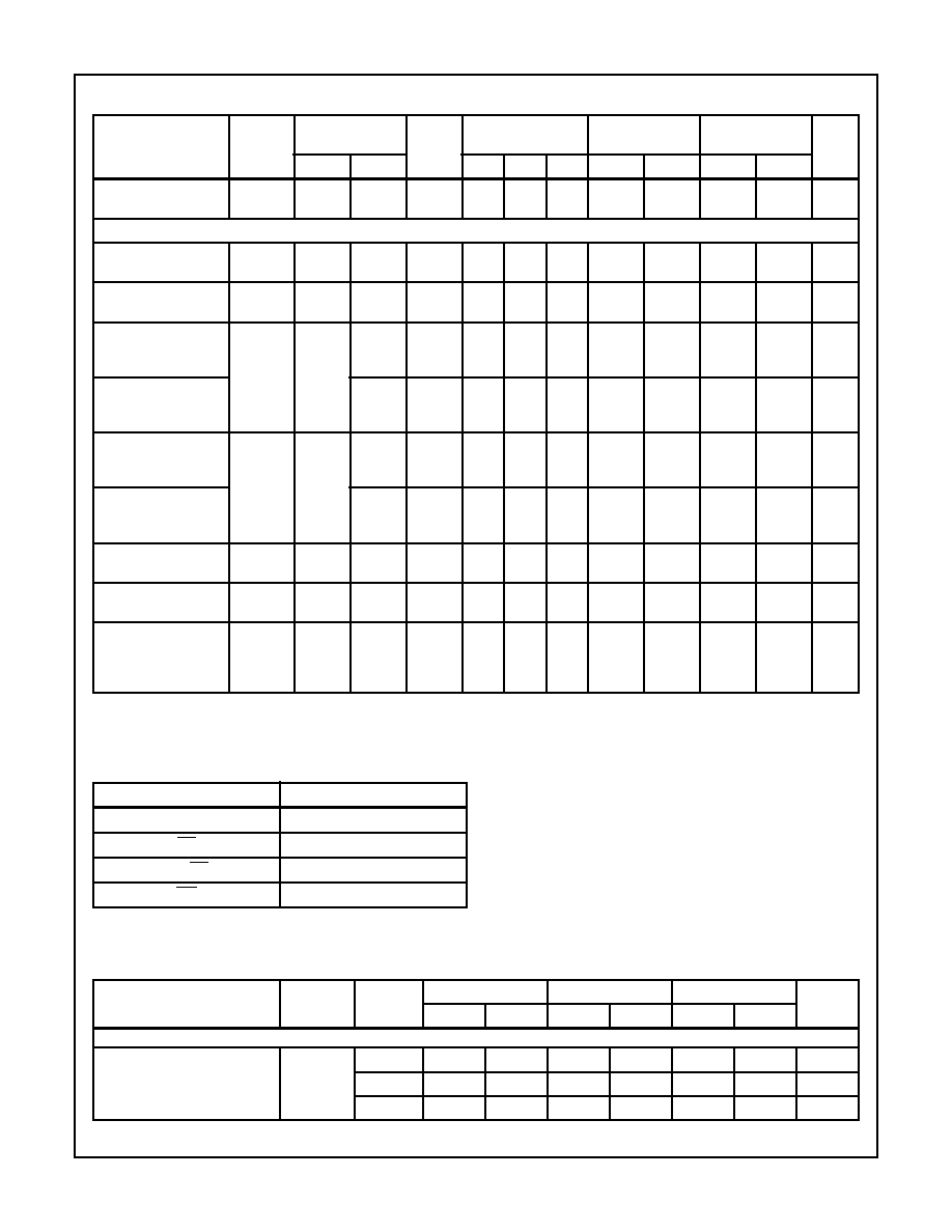
4
Quiescent Device
Current
I
CC
V
CC
or
GND
0
6
-
-
8
-
80
-
160
µ
A
HCT TYPES
High Level Input
Voltage
V
IH
-
-
4.5 to
5.5
2
-
-
2
-
2
-
V
Low Level Input
Voltage
V
IL
-
-
4.5 to
5.5
-
-
0.8
-
0.8
-
0.8
V
High Level Output
Voltage
CMOS Loads
V
OH
V
IH
or
V
IL
-0.02
4.5
4.4
-
-
4.4
-
4.4
-
V
High Level Output
Voltage
TTL Loads
-4
4.5
3.98
-
-
3.84
-
3.7
-
V
Low Level Output
Voltage
CMOS Loads
V
OL
V
IH
or
V
IL
0.02
4.5
-
-
0.1
-
0.1
-
0.1
V
Low Level Output
Voltage
TTL Loads
4
4.5
-
-
0.26
-
0.33
-
0.4
V
Input Leakage
Current
I
I
V
CC
to
GND
0
5.5
-
-
±
0.1
-
±
1
-
±
1
µ
A
Quiescent Device
Current
I
CC
V
CC
or
GND
0
5.5
-
-
8
-
80
-
160
µ
A
Additional Quiescent
Device Current Per
Input Pin: 1 Unit Load
(Note 4)
I
CC
V
CC
-2.1
-
4.5 to
5.5
-
100
360
-
450
-
490
µ
A
NOTE:
4. For dual-supply systems theoretical worst case (V
I
= 2.4V, V
CC
= 5.5V) specification is 1.8mA.
DC Electrical Specifications
(Continued)
PARAMETER
SYMBOL
TEST
CONDITIONS
V
CC
(V)
25
o
C
-40
o
C TO 85
o
C
-55
o
C TO 125
o
C
UNITS
V
I
(V)
I
O
(mA)
MIN
TYP
MAX
MIN
MAX
MIN
MAX
HCT Input Loading Table
INPUT
UNIT LOADS
DS, D0-D7
0.2
PE
0.35
CP, CE
0.5
MR
0.2
NOTE: Unit Load is
I
CC
limit specified in DC Electrical
Specifications table, e.g., 360
µ
A max at 25
o
C.
Prerequisite For Switching Specifications
PARAMETER
SYMBOL
V
CC
(V)
25
o
C
-40
o
C TO 85
o
C
-55
o
C TO 125
o
C
UNITS
MIN
MAX
MIN
MAX
MIN
MAX
HC TYPES
Clock Frequency
(Figure 1)
f
MAX
2
6
-
5
-
4
-
MHz
4.5
30
-
25
-
20
-
MHz
6
35
-
29
-
23
-
MHz
CD74HC166, CD74HCT166
5
MR Pulse Width
(Figure 1)
t
w
2
100
-
125
-
150
-
ns
4.5
20
-
25
-
30
-
ns
6
17
-
21
-
26
-
ns
Clock Pulse Width
(Figure 1)
t
W
2
80
-
100
-
120
-
ns
4.5
16
-
20
-
24
-
ns
6
14
-
17
-
20
-
ns
Set-up Time
Data and CE to Clock
(Figure 5)
t
SU
2
80
-
100
-
120
-
ns
4.5
16
-
20
-
24
-
ns
6
14
-
17
-
20
-
ns
Hold Time
Data to Clock
(Figure 5)
t
H
2
1
-
1
-
1
-
ns
4.5
1
-
1
-
1
-
ns
6
1
-
1
-
1
-
ns
Removal Time
MR to Clock
(Figure 5)
t
REM
2
0
-
0
-
0
-
ns
4.5
0
-
0
-
0
-
ns
6
0
-
0
-
0
-
ns
Set-up Time
PE to CP
(Figure 5)
t
SU
2
145
-
180
-
220
-
ns
4.5
29
-
36
-
44
-
ns
6
25
-
31
-
38
-
ns
Hold Time
PE to CP or CE
(Figure 5)
t
H
2
0
-
0
-
0
-
ns
4.5
0
-
0
-
0
-
ns
6
0
-
0
-
0
-
ns
HCT TYPES
Clock Frequency (Figure 2)
f
MAX
4.5
25
-
20
-
16
-
MHz
MR Pulse Width (Figure 2)
t
w
4.5
35
-
44
-
53
-
ns
Clock Pulse Width (Figure 2)
t
w
4.5
20
-
25
-
30
-
ns
Set-up Time Data and CE to
Clock (Figure 6)
t
SU
4.5
16
-
20
-
24
-
ns
Hold Time Data to Clock
(Figure 6)
t
H
4.5
0
-
0
-
0
-
ns
Removal Time MR to Clock
(Figure 6)
t
REM
4.5
0
-
0
-
0
-
ns
Set-up Time PE to CP (Figure 6)
t
SU
4.5
30
-
38
-
45
-
ns
Hold Time PE to CP or CE
(Figure 6)
t
H
4.5
0
-
0
-
0
-
ns
Switching Specifications
Input t
r
, t
f
= 6ns
PARAMETER
SYMBOL
TEST
CONDITIONS
V
CC
(V)
25
o
C
-40
o
C TO 85
o
C
-55
o
C TO 125
o
C
UNITS
TYP
MAX
MAX
MAX
HC TYPES
Propagation Delay,
Clock to Output (Figure 3)
t
PLH
, t
PHL
C
L
= 50pF
2
-
160
200
240
ns
4.5
-
32
40
48
ns
C
L
= 15pF
5
13
-
-
-
ns
CL = 50pF
6
-
27
34
41
ns
Prerequisite For Switching Specifications
(Continued)
PARAMETER
SYMBOL
V
CC
(V)
25
o
C
-40
o
C TO 85
o
C
-55
o
C TO 125
o
C
UNITS
MIN
MAX
MIN
MAX
MIN
MAX
CD74HC166, CD74HCT166