
Product Description
Stanford Microdevices' SNA-300 is a GaAs monolithic broad-
band amplifier (MMIC) in die form. This amplifier provides
22dB of gain when biased at 35mA and 4V.
External DC decoupling capacitors determine low frequency
response. The use of an external resistor allows for bias
flexibility and stability.
These unconditionally stable amplifiers are designed for use
as general purpose 50 ohm gain blocks. Also available in
packaged form (SNA-376, -386 & -387), its small size (0.33mm
x 0.33mm) and gold metallization make it an ideal choice for
use in hybrid circuits.
The SNA-300 is available in gel paks at 100 devices per
container.
SNA-300
DC-3 GHz, Cascadable
GaAs MMIC Amplifier
Product Features
À
Cascadable 50 Ohm Gain Block
À
22dB Gain, +10dBm P1dB
À
1.5:1 Input and Output VSWR
À
Operates From Single Supply
À
Chip Back is Ground
Applications
À
Narrow and Broadband Linear Amplifiers
À
Commercial and Industrial Applications
S y m b o l
P a r a m e t e r s : T e s t C o n d i t i o n s :
I d = 3 5 m A , Z
0
= 5 0 O h m s
U n i t s
M i n .
T y p .
M a x .
G
P
S m a l l S i g n a l P o w e r G a i n
f = 0 . 1 - 1 . 0 G H z
f = 1 . 0 - 2 . 0 G H z
f = 2 . 0 - 3 . 0 G H z
d B
d B
d B
2 1 . 0
2 0 . 0
1 9 . 0
2 3 . 0
2 2 . 0
2 1 . 0
G
F
G a i n F l a t n e s s
f = 0 . 1 - 3 . 0 G H z
d B
+ / - 1 . 5
B W 3 d B
3 d B B a n d w i d t h
G H z
3 . 0
P
1 d B
O u t p u t P o w e r a t 1 d B C o m p r e s s i o n
f = 2 . 0 G H z
d B m
1 0 . 0
N F
N o i s e F i g u r e
f = 2 . 0 G H z
d B
4 . 0
5 . 0
V S W R
I n p u t / O u t p u t
f = 0 . 1 - 3 . 0 G H z
1 . 5 : 1
I P
3
T h i r d O r d e r I n t e r c e p t P o i n t
f = 2 . 0 G H z
d B m
2 3 . 0
T
D
G r o u p D e l a y
f = 2 . 0 G H z
p s e c
1 0 0
I S O L
R e v e r s e I s o l a t i o n
f = 0 . 1 - 3 . 0 G H z
d B
2 2 . 0
V D
D e v i c e V o l t a g e
V
3 . 5
4 . 0
4 . 5
d G / d T
D e v i c e G a i n T e m p e r a t u r e C o e f f i c i e n t
d B / d e g C
- 0 . 0 0 3
d V / d T
D e v i c e V o l t a g e T e m p e r a t u r e C o e f f i c i e n t
m V / d e g C
- 4 . 0
The information provided herein is believed to be reliable at press time. Stanford Microdevices assumes no responsibility for inaccuracies or omissions.
Stanford Microdevices assumes no responsibility for the use of this information, and all such information shall be entirely at the user's own risk. Prices and specifications are subject to change
without notice. No patent rights or licenses to any of the circuits described herein are implied or granted to any third party. Stanford Microdevices does not authorize or warrant any Stanford
Microdevices product for use in life-support devices and/or systems.
Copyright 1999 Stanford Microdevices, Inc. All worldwide rights reserved.
522 Almanor Ave., Sunnyvale, CA 94086 Phone: (800) SMI-MMIC http://www.stanfordmicro.com
Electrical Specifications at Ta = 25C
Output Power vs. Frequency
8
9
10
11
12
0.1
0.5
1
1.5
2
4
6
8
10
GHz
dBm
5-37
50 Ohm Gain Blocks
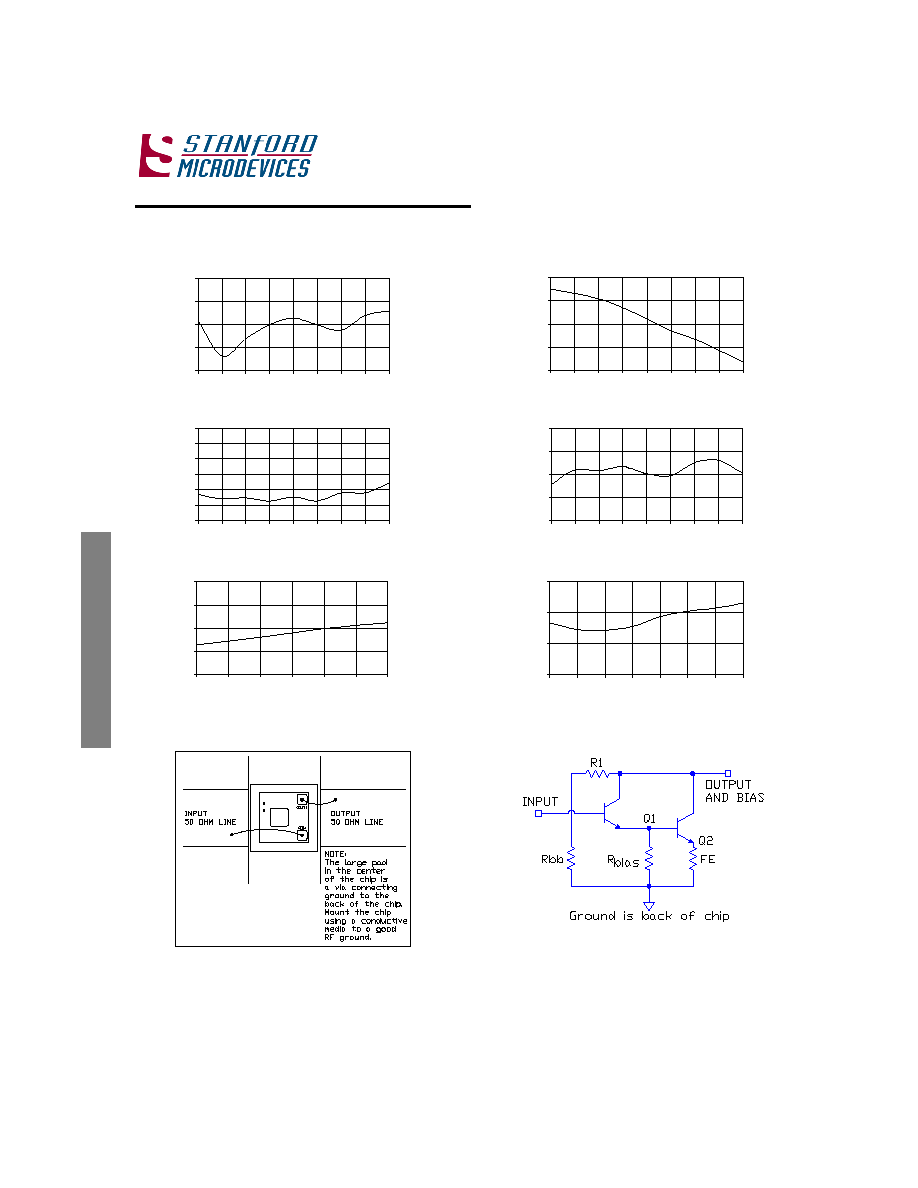
Noise Figure vs. Frequency
3
3.5
4
4.5
5
0.1
0.5
1.0
1.5
2.0
2.5
3.0
SNA-300 DC-3 GHz Cascadable MMIC Amplifier
Typical Performance at 25
░░
░░
░
C (Vds = 4.0V, Ids = 35mA)
522 Almanor Ave., Sunnyvale, CA 94086 Phone: (800) SMI-MMIC http://www.stanfordmicro.com
50 Ohm Gain Blocks
GHz
dB
|S11| vs. Frequency
|S21| vs. Frequency
|S12| vs. Frequency
|S22| vs. Frequency
TOIP vs. Frequency
-40
-30
-20
-10
0
0.1
0.5
1
1.5
2
2.5
3
3.5
4
-30
-25
-20
-15
-10
-5
0
0.1
0.5
1
1.5
2
2.5
3
3.5
4
15
17
19
21
23
0.1
0.5
1
1.5
2
2.5
3
3.5
4
-40
-30
-20
-10
0
0.1
0.5
1
1.5
2
2.5
3
3.5
4
20
22
24
26
0.5
1
1.5
2
2.5
3
3.5
4
GHz
dB
dBm
GHz
dB
GHz
dB
GHz
dB
GHz
Suggested Bonding Arrangement
Simplified Schematic of MMIC
5-38

SNA-300 DC-3 GHz Cascadable MMIC Amplifier
Absolute Maximum Ratings
Part Number
Devices Per Pak
SNA-300
100
Part Number Ordering Information
522 Almanor Ave., Sunnyvale, CA 94086 Phone: (800) SMI-MMIC http://www.stanfordmicro.com
Typical Biasing Configuration
Notes:
1. Operation of this device above any one of these
parameters may cause permanent damage.
MTTF vs. Temperature @ Id = 35mA
Thermal Resistance (Lead-Junction): 407░ C/W
P a r a m e te r
A b s o lu te
M a x im u m
D e vic e C ur re nt
9 0 m A
P o w e r D issipa tion
4 0 0m W
R F In p ut P o w er
2 0 m W
Ju n ction Te m p e ra ture
+2 0 0 C
O p e ra tin g Te m p e ra tu re
-4 5 C to +8 5 C
S to ra g e Te m pe ra tu re
-6 5 C to +1 5 0 C
Die Bottom
Temperature
Junction
Temperature
MTTF (hrs)
+65C
+120C
10000000
+100C
+155C
1000000
+135C
+190C
100000
50 Ohm Gain Blocks
Die Attach
The die attach process mechanically attaches the die to
the circuit substrate. In addition, it electrically connects
the ground to the trace on which the die is mounted and
establishes the thermal path by which heat can leave the
die.
Assembly Techniques
Epoxy die attach is recommended. The top and bottom
metallization is gold. Conductive silver-filled epoxies are
recommended. This method involves the use of epoxy to
form a joint between the backside gold of the chip and
the metallized area of the substrate. A 150 C cure for 1
hour is necessary. Recommended epoxy is Ablebond
84-1LMIT1 from Ablestik.
Wire Bonding
Electrical connections to the die are through wire
bonds. Stanford Microdevices recommends wedge
bonding or ball bonding to the pads of these devices.
Recommended Wedge Bonding Procedure
1. Set the heater block temperature to 260C +/- 10C.
2. Use pre-stressed (annealed) gold wire between
0.0005 to 0.001 inches in diameter.
3. Tip bonding pressure should be between 15 and
20 grams and should not exceed 20 grams. The
footprint that the wedge leaves on the gold wire
should be between 1.5 and 2.5 wire diameters
across for a good bond.
5-39