01-OVERV.PDF

KS57C0404/C0408/P0408 MICROCONTROLLER
PRODUCT OVERVIEW
11
1
PRODUCT OVERVIEW
The KS57C0404/C0408 single-chip CMOS microcontroller has been designed for very high-performance using
Samsung's newest 4-bit CPU core, SAM47 (Samsung Arrangeable Microcontrollers).
The KS57P0408 is the microcontroller which has 8K-bytes one-time-programmable ROM and the functions are
same to KS57C0404/C0408.
With two 8-bit timer/counters, an 8-bit serial I/O interface, and eight software n-channel open-drain I/O pins, the
KS57C0404/C0408 offers an excellent design solution for a wide variety of general-purpose applications.
Up to 36 pins of the 42-pin SDIP or 44-pin QFP package can be dedicated to I/O. Seven vectored interrupts
provide fast response to internal and external events.
In addition, the KS57C0404/C0408's advanced CMOS technology provides for low power consumption and a
wide operating voltage range.

PRODUCT OVERVIEW
KS57C0404/C0408/P0408 MICROCONTROLLER
12
FEATURES SUMMARY
Memory
·
512
×
4-bit RAM
·
4096
×
8-bit ROM: KS57C0404
·
8192
×
8-bit ROM: KS57C0408
36 I/O Pins
·
Input only: 4 pins
·
I/O: 24 pins
·
N-channel open-drain I/O: 8 pins
Memory-Mapped I/O Structure
·
Data memory bank 15
8-Bit Basic Timer
·
4 interval timer functions
Two 8-Bit Timer/Counters
·
Programmable interval timer
·
External event counter function
·
Timer/counters clock outputs to TCLO0 and
TCLO1 pins
Watch Timer
·
Time interval generation: 0.5 s, 3.9 ms at
4.19 MHz
·
4 frequency outputs to the BUZ pin
8-Bit Serial I/O Interface
·
8-bit transmit/receive mode
·
8-bit receive mode
·
LSB-first or MSB-first transmission selectable
Bit Sequential Carrier
·
Supports 16-bit serial data transfer in arbitrary
format
Interrupts
·
3 external interrupt vectors
·
4 internal interrupt vectors
·
2 quasi-interrupts
Power-Down Modes
·
Idle: Only CPU clock stops
·
Stop: System clock stops
Oscillation Sources
·
Crystal or Ceramic for system clock
·
Oscillation frequency : 0.4 6.0MHz
·
CPU clock divider circuit (by 4. 8, or 64)
Instruction Execution Times
·
0.95, 1.91, 15.3
µ
s at 4.19 MHz
·
0.67, 1.33, 10.7
µ
s at 6.0 MHz
Operating Temperature
·
- 40
°
C to 85
°
C
Operating Voltage Range
·
1.8 V to 5.5 V (Main)
·
2.0 V to 5.5 V (OTP)
Package Types
·
42-pin SDIP, 44-pin QFP

KS57C0404/C0408/P0408 MICROCONTROLLER
PRODUCT OVERVIEW
13
FUNCTION OVERVIEW
SAM47 CPU
All KS57-series microcontrollers have the advanced SAM47 CPU core. The SAM47 CPU can directly address up
to 32K-byte of program memory. The arithmetic logic unit(ALU) performs 4-bit addition, subtraction, logical, and
shift-and-rotate operations in one instruction cycle and most 8-bit arithmetic and logical operation in two cycles.
CPU REGISTERS
program counter
A 12-bit program counter (PC) stores addresses for instruction fetches during program execution. Usually, the PC
is incremented by the number of bytes of the fetched instruction. The one instruction fetch that does not
increment the PC is the 1-byte REF instruction which references instruction stored in a look-up table in the ROM.
Whenever a reset operation or an interrupt occurs, bits PC12 though PC0 are set to the vector address.
Stack pointer
An 8-bit stack pointer (SP) stores addresses for stack operation. The stack area is located in general-purpose
data memory bank 0. The SP is 8-bit read/writeable and SP bit 0 must always be logic zero.
During an interrupt or a subroutine call, the PC value and the PSW are written to the stack area. When the
service routine has completed, the values referenced by the stack pointer are restored. Then, the next instruction
is executed.
The stack pointer can access the stack despite data memory access enable flag status. Since the reset value of
the stack pointer is not defined in firmware, you use program code to initialize the stack pointer to 00H. This sets
the first register of the stack area to data memory location 0FFH.
PROGRAM MEMORY
In its standard configuration, the 4096 x 8-bit (KS57C0404), 8192 x 8-bit (KS57C0408) ROM is divided into four
areas:
16-byte area for vector addresses
96-byte instruction reference area
16-byte general-purpose area (0010 001FH)
3968-byte area for general-purpose program memory (KS57C0404)
8064-byte area for general-purpose program memory (KS57C0408)
The vector address area is used mostly during reset operation and interrupts. These 16 bytes can alternately be
used as general-purpose ROM.
The REF instruction references 2x1-byte or 2-byte instruction stored in reference area location 0020H 007FH.
REF can also reference three-byte instruction such as JP or CALL. So that a REF instruction can reference these
instruction, however, the JP or CALL must be shortened to a 2-byte format. To do this, JP or CALL is written to
the reference area with the format TJP or TCALL instead of the normal instruction name. Unused location in the
REF instruction look-up area can be allocated to general-purpose use.

PRODUCT OVERVIEW
KS57C0404/C0408/P0408 MICROCONTROLLER
14
DATA MEMORY
Overview
The 512 x 4bit data memory has five areas:
32 x 4-bit working register area
224 x 4-bit general-purpose area in bank 0 which is also used as the stack area
256 x 4-bit general-purpose area in bank 1
128 x 4-bit area in bank 15 for memory-mapped I/O addresses
The data memory area is also organized as three memory banks
bank0, bank1, and bank15. You use the
select memory bank instruction (SMB) to select one of the banks as working data memory.
Data stored in RAM location are 1-, 4-, and 8-bit addressable. After a hardware reset, data memory initialization
values must be defined by program code.
Data Memory addressing modes
The enable memory bank (EMB) flag controls the addressing mode for data memory banks 0, 1, or 15. When the
EMB flag is logic zero, only location 00H7FH of bank 0 and bank 15 can be accessed. When the EMB flag is set
to logic one, all three data memory banks can be accessed based on the current SMB value.
Working registers
The RAM's working register area in data memory bank 0 is also divided into four register banks. Each register
bank has eight 4-bit registers. Paired 4-bit registers are 8-bit addressable.
Register A can be used as a 4-bit accumulator and double register EA as an 8-bit extended accumulator; double
registers WX, WL, and HL are used as address pointers for indirect addressing.
To limit the possibility of data corruption due to incorrect register addressing, it is advisable to use bank 0 for
main programs and banks 1, 2, and 3 for interrupt service routines.
Bit sequential carrier
The bit sequential carrier (BSC) mapped in data memory bank 15 is a 16-bit general register that you can
manipulate using 1-, 4-, and 8-bit RAM control instructions.
Using the BSC register, addresses and bit location can be specified sequentially using 1-bit indirect addressing
instructions. In this way, a program can generate 16-bit data output by moving the bit location sequentially,
incrementing or decrementing the value of the L register. You can also use direct addressing to manipulate data
in the BSC.
KS57C0404/C0408/P0408 MICROCONTROLLER
PRODUCT OVERVIEW
15
CONTROL REGISTERS
Program Status Word
The 8-bit program status word (PSW) controls ALU operation and instruction execution sequencing. It is also
used to restore a program's execution environment when an interrupt has been serviced. Program instructions
can always address the PSW regardless of the current value of data memory access enable flags.
Before an interrupt is processed, the PSW is pushed onto the stack in data memory bank 0. When the routine is
completed, PSW values are restored.
IS1
IS0
EMB
ERB
C
SC2
SC1
SC0
Interrupt status flags (IS1, IS0), the enable memory bank and enable register bank flags (EMB, ERB), and the
carry flag ( C ) are 1- and 4-bit read/write or 8-bit read-only addressable. Skip condition flags (SC0SC2) can be
addressed using 8-bit read instructions only.
Select Bank (SB) Register
Two 4-bit location called the SB register store address values used to access specific memory and register
banks: the select memory bank register, SMB, and the select register bank register, SRB.
'SMB n' instructions select a data memory bank (0, 1, or 15) and store the upper four bits of the 12-bit data
memory address in the SMB register. The 'SMB n' instruction is used to select register bank 0, 1, 2, or 3, and to
store the address data in the SRB.
The instructions 'PUSH SB' and 'POP SB' move SMB and SRB values to and from the stack for interrupts and
subroutines.
CLOCK CIRCUITS
System oscillation circuit generates the internal clock signals for the CPU and peripheral hardwares. The system
clock can use a crystal, ceramic, or RC oscillation source, or an externally-generated clock signal. To drive
KS57C0404/C0408 using an external clock source, the external clock signal should be input to Xin, and its
inverted signal to Xout.
A 4-bit power control register is used to enable or disable oscillation, and to select the CPU clock. The internal
system clock signal (fx) can be divided internally to produce three CPU clock frequencies
fx/4, fx/8, or fx/64.
INTERRUPTS
Interrupt requests can be generated internally by on-chip processes (INTB, INTT0, INTT1, and INTS) or
externally by peripheral devices (INT0, INT1, and INT4). There are two quasi-interrupts: INT2 and INTW.
INT2/KS0KS7 detects rising/falling edges of incoming signals and INTW detects time intervals of 0.5 seconds of
3.91 milliseconds at 4.19MHz. The following components support interrupt processing:
Interrupt enable flags
Interrupt request flags
Interrupt priority registers
Power-down termination circuit

PRODUCT OVERVIEW
KS57C0404/C0408/P0408 MICROCONTROLLER
16
POWER-DOWN
To reduce power consumption, there are two power-down modes: idle and stop. The IDLE instruction initiates idle
mode and the STOP instruction initiates stop mode.
In idle mode, only the CPU clock stops while peripherals and the oscillation source continue to operate normally.
Stop mode effects only the system clock. In stop mode system clock oscillation stops completely, halting all
operations except for a few basic peripheral functions.
RESET
or an interrupt (with the exception of INT0) can be
used to terminate either idle or stop mode.
RESET
When a
RESET
signal occurs during normal operation or during power-down mode, the CPU enters idle mode
when the reset operation is initiated. When the standard oscillation stabilization interval (31.3 ms at 4.19 MHz)
has elapsed, normal CPU operation resumes.
I/O PORTS
The KS57C0404/C0408 has 9 I/O ports. Pin addresses for all I/O ports are mapped to locations FF0HFFCH in
bank 15 of the RAM.
There are 4 input pins, 24 configurable I/O pins, and 8 software n-channel open-drain I/O pins, for a total of 36
I/O pins. The contents of I/O port pin latches can be read, writen, or tested at the corresponding address using
bit manipulation instructions.
TIMERS AND TIMER/COUNTERS
The timer function has four main components: an 8-bit basic interval timer, two 8-bit timer/counters, and a watch
timer. The 8-bit basic timer generates interrupt requests at precise intervals, based on the selected CPU clock
frequency.
The programmable 8-bit timer/counters are used for external event counting, generation of arbitrary clock
frequencies for output, and dividing external clock signals. The 8-bit timer/counter 0 generates a clock signal
(
SCK
) for the serial I/O interface.
The watch timer has an 8-bit watch timer mode register, a clock selector, and a frequency divider circuit. Its
functions include real-time and watch-time measurement, and frequency outputs for buzzer sound.
SERIAL I/O INTERFACE
The serial I/O interface supports the transmission or reception of 8-bit serial data with an external device. The
serial interface has the following functional components:
8-bit mode register
Clock selector circuit
8-bit buffer register
3-bit serial clock counter
The serial I/O circuit can be set either to transmit-and-receive or to receive-only mode. MSB-first or LSB-first
transmission is also selectable. The serial interface operates with an internal or an external clock source, or using
the clock signal generated by the 8-bit timer/counter 0. To modify transmission frequency, the appropriate bits in
the serial I/O mode register (SMOD) must be manipulated.
KS57C0404/C0408/P0408 MICROCONTROLLER PRODUCT OVERVIEW
17
BLOCK DIAGRAM
P4.0 - 4.3
P5.0 - 5.3
P6.0 - 6.3 /
KS0 - S3
P7.0 - 7.3 /
KS4 - S7
ARITHMETIC
AND
LOGIC UNIT
INTERRUPT
CONTROL
BLOCK
INSTRUCTION
REGISTER
PROGRAM
COUNTER
PROGRAM
STATUS WORD
512 x 4-BIT
DATA
MEMORY
PROGRAM MEMORY
4 KBYTE: KS57C0404
8 KBYTE: KS57C0408
8-BIT
TIMER/
COUNTER 0
STACK
POINTER
INSTRUCTION DECODER
CLOCK
RESET
Xin Xout
INTERNAL
INTERRUPTS
I/O PORT 4
I/O PORT 5
8-BIT
TIMER/
COUNTER 1
I/O PORT 6
I/O PORT 7
INT0, INT1,
INT2,INT4
BASIC
TIMER
WATCH
TIMER
P0.0 /
SCK
P0.1 / SO
P0.2 / SI
P0.3 / BTCO
I/O PORT 0
SERIAL
I/O
P1.0 / INT0
P1.1 / INT1
P1.2 / INT2
P1.3 / INT4
INPUT
PORT 1
P2.0 / TCLO0
P2.1 / TCLO1
P2.2 / CLO
P2.3 / BUZ
I/O PORT 2
P3.0 / TCL0
P3.1 / TCL1
P3.2
P3.3
I/O PORT 3
P8.0 - 8.3
I/O PORT 8
Figure 11. KS57C0404/C0408/P0408 Block Diagram
PRODUCT OVERVIEW
KS57C0404/C0408/P0408 MICROCONTROLLER
18
PIN ASSIGNMENTS
NC
P8.0
P8.1
P8.2
P8.3
P0.0 /
SCK
P0.1 / SO
P0.2 / SI
P0.3 / BTCO
P2.0 / TCLO0
P2.1 / TCLO1
VSS
P7.0 / KS4
P7.1 / KS5
P7.2 / KS6
P7.3 / KS7
P6.0 / KS0
P6.1 / KS1
P6.2 / KS2
P6.3 / KS3
Xin
Xout
RESET
P5.0
P5.1
P5.2
P5.3
P4.0
P4.1
P4.2
P4.3
TEST
42
41
40
39
38
37
36
35
34
33
32
31
30
29
28
27
26
25
24
23
22
1
2
3
4
5
6
7
8
9
10
11
12
13
14
15
16
17
18
19
20
21
P1.3 / INT4
P1.2 / INT2
P1.1 / INT1
P1.0 / INT0
P2.3 / BUZ
P2.2 / CLO
P2.1 / TCLO1
P2.0 / TCLO0
P0.3 / BTCO
P0.2 / SI
P0.1 / SO
P0.0 /
SCK
P8.3
P8.2
P8.1
P8.0
P3.3
P3.2
P3.1 / TCL1
P3.0 / TCL0
VDD
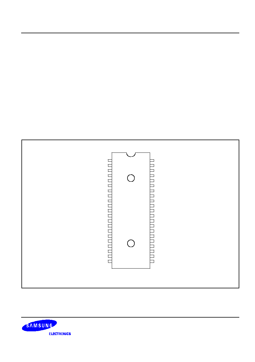
KS57C0404/C0408
(42-SDIP-600)
P2.2 / CLO
P2.3 / BUZ
P1.0 / INT0
P1.1 / INT1
P1.2 / INT2
P1.3 / INT4
VSS
P7.0 / KS4
P7.1 / KS5
P7.2 / KS6
P7.3 / KS7
34
35
36
37
38
39
40
41
42
43
44
22
21
20
19
18
17
16
15
14
13
12
NC
P3.3
P3.2
P3.1 / TCL1
P3.0 / TCL0
VDD
TEST
P4.3
P4.2
P4.1
P4.0
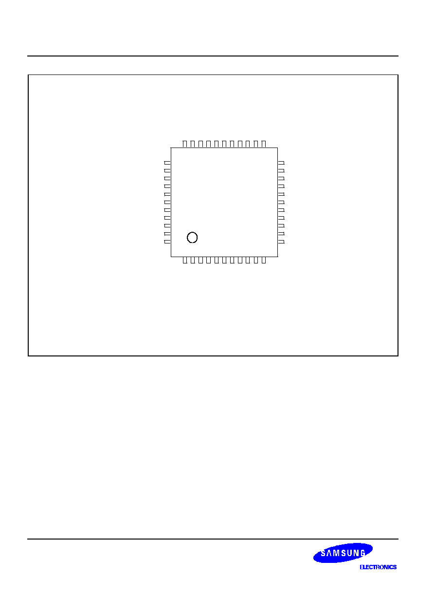
KS57C0404/C0408
(44-QFP-1010B)
1
2
3
4
5
6
7
8
9
10
11
33
32
31
30
29
28
27
26
25
24
23
P5.3
P5.2
P5.1
P5.0
RESET
Xout
Xin
P6.3/KS3
P6.2/KS2
P6.1/KS1
P6.0/KS0
Figure 12. KS57C0404/C0408 Pin Assignment Diagrams
KS57C0404/C0408/P0408 MICROCONTROLLER
PRODUCT OVERVIEW
19
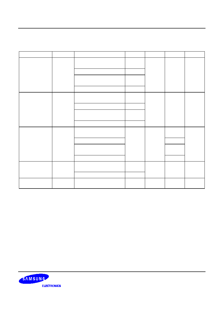
PIN DESCRIPTI/ONS
Table 11. KS57C0404/C0408/P0408 Pin Description
Pin Name
Pin Type
Description
Number
Share Pin
P0.0
P0.1
P0.2
P0.3
I/O
4-bit I/O port.
1-bit or 4-bit read/write and test is possible.
Individual pins are software configurable as input or
output.
4-bit pull-up resistors are software assignable; pull-up
resistors are automatically disabled for output pins.
12 (28)
11 (27)
10 (26)
9 (25)
SCK
SO
SI
BTCO
P1.0
P1.1
P1.2
P1.3
I
4-bit input port.
1-bit and 4-bit read and test is possible.
3-bit pull-up resistors are assignable by software to
pins P1.0, P1.1, and P1.2.
4 (20)
3 (19)
2 (18)
1 (17)
INT0
INT1
INT2
INT4
P2.0
P2.1
P2.2
P2.3
I/O
Same as port 0.
8 (24)
7 (23)
6 (22)
5 (21)
TCLO0
TCLO1
CLO
BUZ
P3.0
P3.1
P3.2
P3.3
I/O
Same as port 0.
20 (38)
19 (37)
18 (36)
17 (35)
TCL0
TCL1
P4.0P4.3
P5.0P5.3
I/O
4-bit I/O ports.
N-channel open-drain output up to 9 volts.
1-bit and 4-bit read/write and test is possible.
Ports 4 and 5 can be paired to support 8-bit data
transfer.
8-bit unit pull-up resistors are assignable by mask
option.
2623
(4441)
3027
(41)
P6.0P6.3
P7.0P7.3
I/O
4-bit I/O ports.
1-bit or 4-bit read/write and test is possible.
Port 6 pins are individually software configurable as
input or output.
4-bit pull-up resistors are software assignable; pull-up
resistors are automatically disabled for output pins
(port 6 only).
Ports 6 and 7 can be paired to enable 8-bit data
transfer.
3734
(118)
4138
(1512)
KS0KS3
KS4KS7
P8.0P8.3
I/O
4-bit I/O ports.
1-bit and 4-bit read/write and test is possible.
Pins are individually software configurable as input or
output.
4-bit pull-down resistors are software assignable;
pull-down resistors are automatically disabled for
output pins.
1613
(3229)
NOTE:
Parentheses indicate pin number for 44 QFP package.
PRODUCT OVERVIEW
KS57C0404/C0408/P0408 MICROCONTROLLER
110
Table 11. KS57C0404/C0408 Pin Descriptions (Continued)
Pin Name
Pin Type
Description
Number
Share
Pin
SCK
I/O
Serial I/O interface clock signal
12 (28)
P0.0
SO
I/O
Serial data output
11 (27)
P0.1
SI
I/O
Serial data input
10 (26)
P0.2
BTCO
I/O
Basic timer clock output (2 Hz, 16 Hz, 64 Hz, or 256
Hz at 4.19 MHz)
9 (25)
P0.3
INT0, INT1
I
External interrupts. The triggering edge for INT0 and
INT1 is selectable. INT0 is synchronized to system
clock.
4, 3
(20, 19)
P1.0, P1.1
INT2
I
Quasi-interrupt with detection of rising edges
2 (18)
P1.2
INT4
I
External interrupt with detection of rising and falling
edges.
1 (17)
P1.3
TCLO0
I/O
Timer/counter 0 clock output
8 (24)
P2.0
TCLO1
I/O
Timer/counter 1 clock output
7 (23)
P2.1
CLO
I/O
Clock output
6 (22)
P2.2
BUZ
I/O
2 kHz, 4 kHz, 8 kHz, or 16 kHz frequency output at
4.19 MHz for buzzer sound
5 (21)
P2.3
TCL0
I/O
External clock input for timer/counter 0
20 (38)
P3.0
TCL1
I/O
External clock input for timer/counter 1
19 (37)
P3.1
KS0KS3
KS4KS7
I/O
Quasi-interrupt inputs with falling edge detection
3734
(118)
4138
(1512)
P6.0P6.3
P7.0P7.3
V
DD
Power supply
21 (39)
V
SS
Ground
42 (16)
RESET
I
Reset signal
31 (5)
X
in
, X
out
Crystal, ceramic, or RC oscillator signal for system
clock (For external clock input, use X
in
and input
X
in
's reverse phase to X
out
)
33, 32
(7, 6)
TEST
Test signal input (must be connected to V
SS
)
22 (40)
NC
No connection (must be connected to V
SS
)
(33, 34)
NOTE:
Parentheses indicate pin number for 44 QFP package.
KS57C0404/C0408/P0408 MICROCONTROLLER
PRODUCT OVERVIEW
111
Table 12. Overview of KS57C0404/C0408 Pin Data
Pin Names
Share Pins
I/O Type
Reset Value
Circuit Type
P0.0P0.3
SCK
, SO, SI, BTCO
I/O
Input
D-1
P1.0P1.2
INT0, INT1, INT2
I
Input
A-3
P1.3
INT4
I
Input
B-4
P2.0P2.3
TCLO0, TCLO1, CLO,
BUZ
I/O
Input
D
P3.0P3.1
TCL0, TCL1
I/O
Input
D-1
P3.2P3.3
I/O
Input
D
P4.0P4.3
P5.0P5.3
I/O
(NOTE)
E-2
P6.0P6.3
P7.0P7.3
KS0KS3
KS4KS7
I/O
Input
D-1
P8.0P8.3
I/O
Input
D-2
X
in
, X
out
RESET
I
B
TEST
I
NC
V
DD
, V
SS
NOTE: When pull-up resistors are provided, port 4 and port 5 pins are reset to high level; with no pull-ups, they are reset to
high impedance.
PRODUCT OVERVIEW
KS57C0404/C0408/P0408 MICROCONTROLLER
112
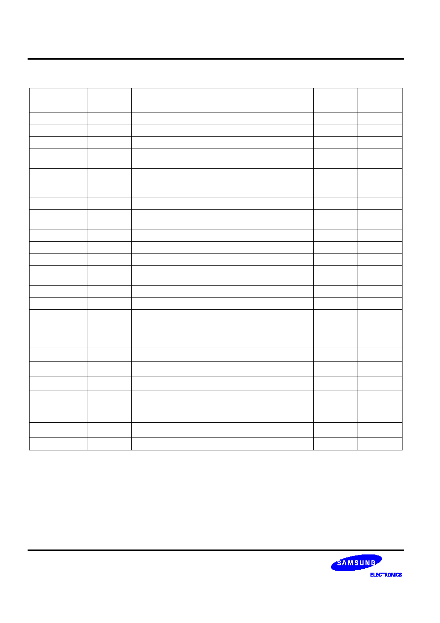
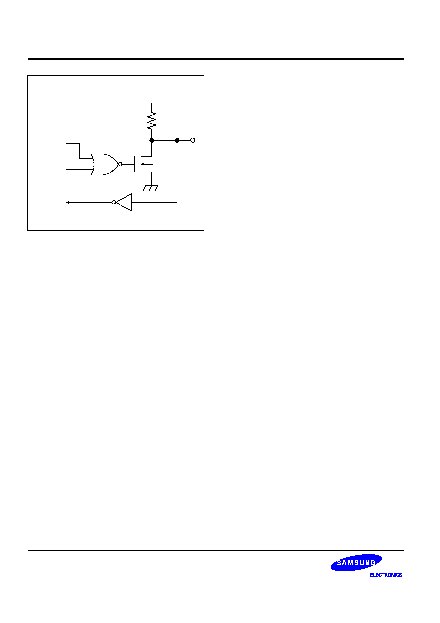
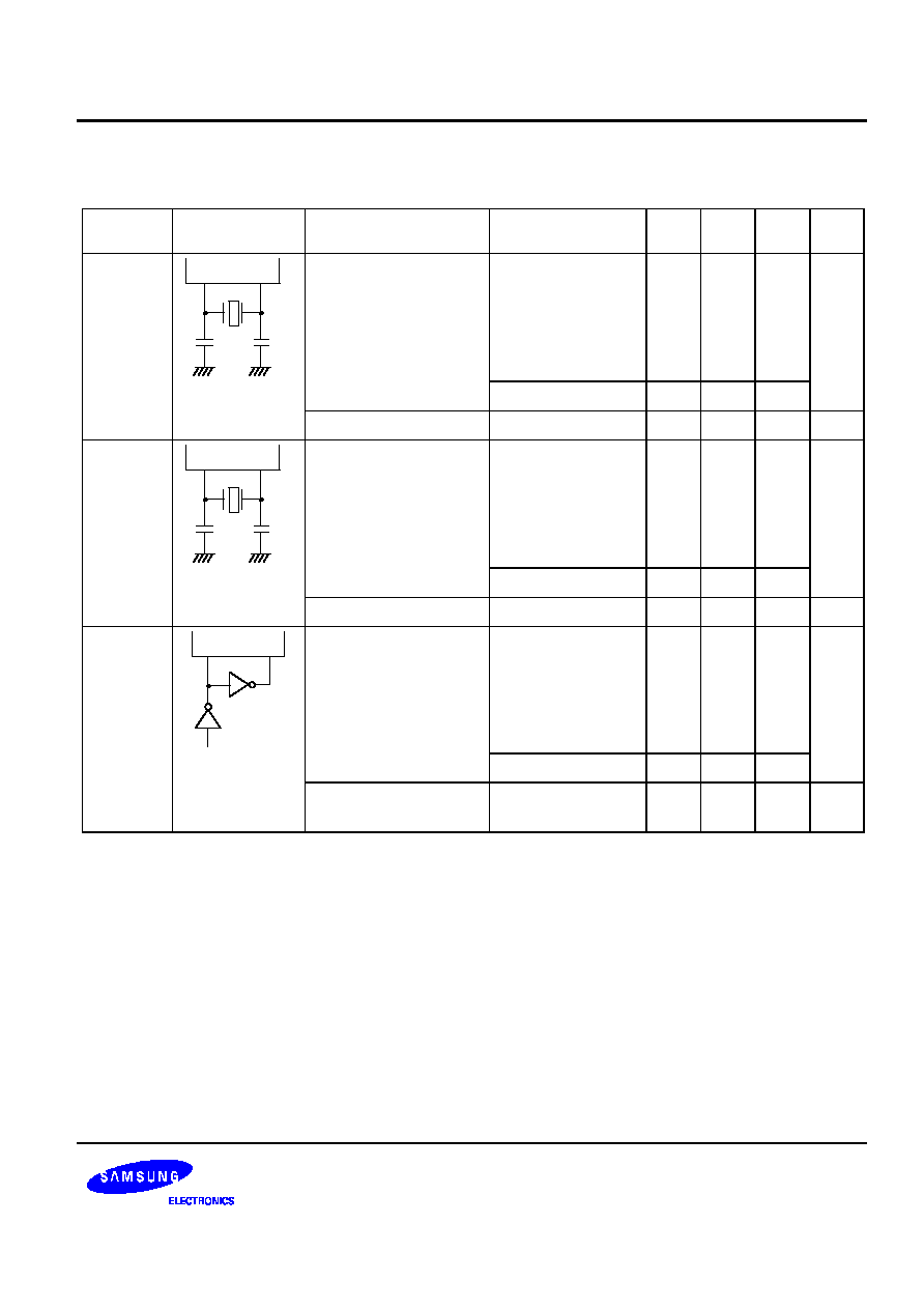
PIN CIRCUIT DIAGRAMS
P
-
CHANNEL
IN
N
-
CHANNEL
V
DD
Figure 13. Pin Circuit Type A
P
-
CHANNEL
PULL-UP
RESISTOR
PULL-UP RESISTOR
ENABLE
SCHMITT TRIGGER
IN
V
DD
Figure 14. Pin Circuit Type A3
IN
V
DD
PULL-UP
RESISTOR
SCHMITT TRIGGER
Figure 15. Pin Circuit Type B
SCHMITT TRIGGER
IN
Figure 16. Pin Circuit Type B4
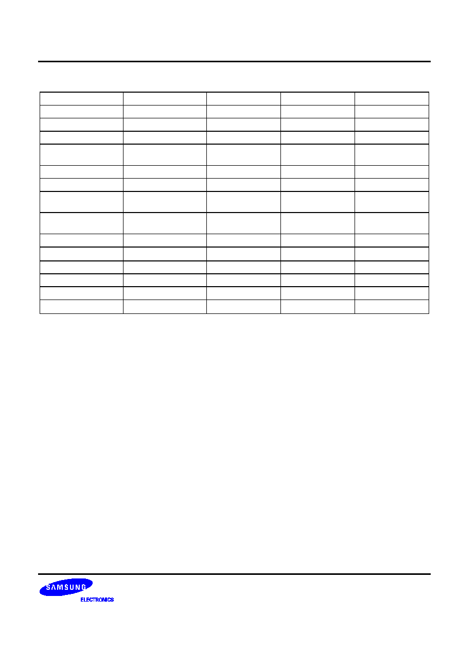
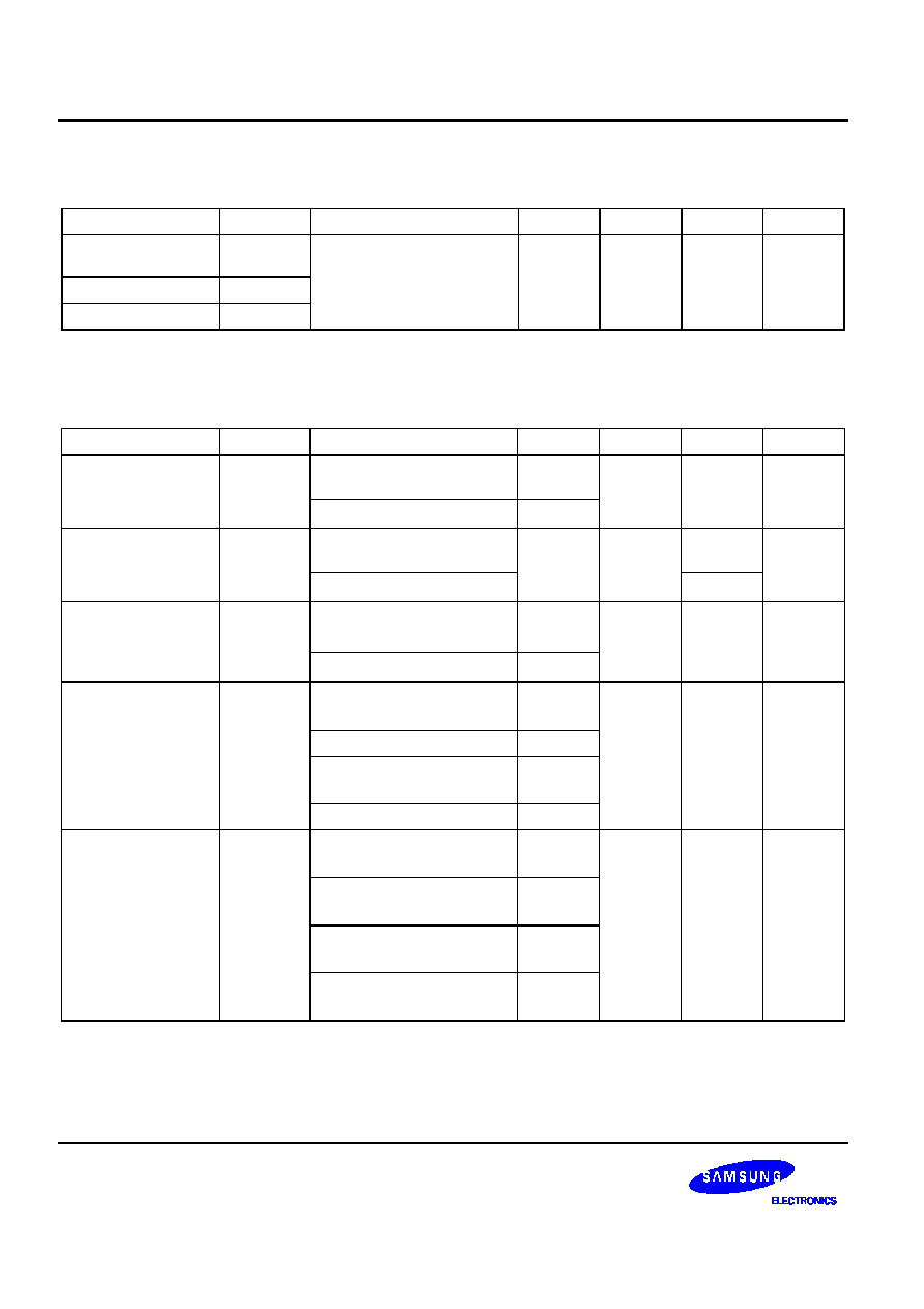
KS57C0404/C0408/P0408 MICROCONTROLLER
PRODUCT OVERVIEW
113
P
-
CHANNEL
DATA
OUTPUT
DISABLE
OUT
N
-
CHANNEL
V
DD
Figure 17. Pin Circuit Type C
P
-
CHANNEL
PULL-UP
RESISTOR
RESISTOR
ENABLE
CIRCUIT
TYPE C
DATA
OUTPUT
DISABLE
CIRCUIT TYPE A
I/O
V
DD
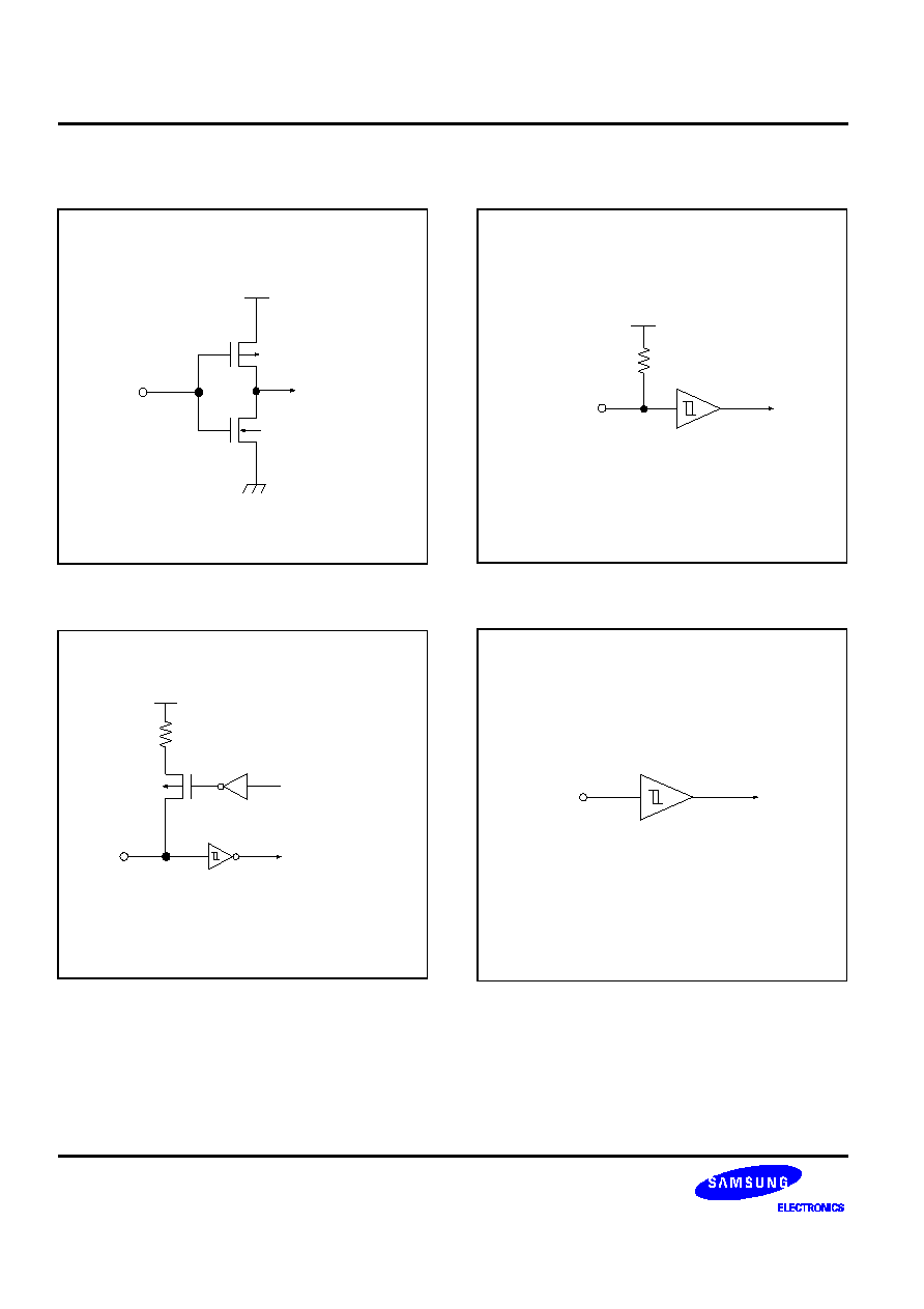
Figure 18. Pin Circuit Type D
P
-
CHANNEL
PULL-UP
RESISTOR
RESISTOR
ENABLE
CIRCUIT
TYPE C
DATA
OUTPUT
DISABLE
SCHMITT TRIGGER
I/O
V
DD
Figure 19. Pin Circuit Type D-1
N
-
CHANNEL
PULL-DOWN
RESISTOR
RESISTOR
ENABLE
CIRCUIT
TYPE C
DATA
OUTPUT
DISABLE
CIRCUIT TYPE A
I/O
Figure 110. Pin Circuit Type D2
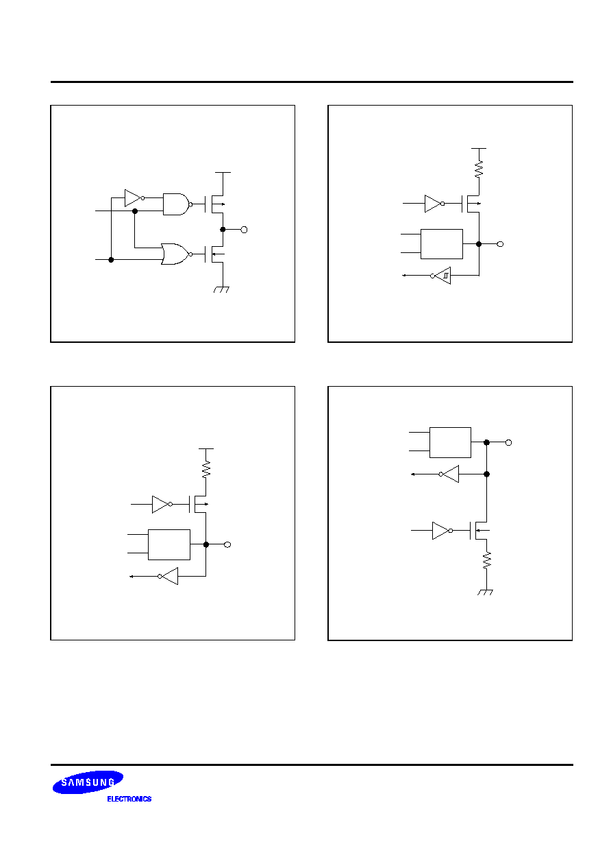
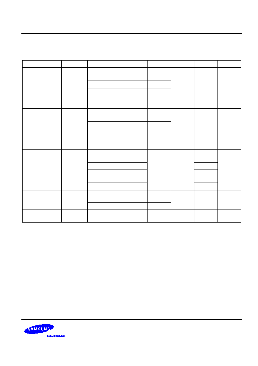
PRODUCT OVERVIEW
KS57C0404/C0408/P0408 MICROCONTROLLER
114
DATA
OUTPUT
DISABLE
VDD
I/O
N-CHANNEL
Figure 111. Pin Circuit Type E-2

KS57C0404/C0408/P0408 MICROCONTROLLER
ELECTRICAL DATA
131
13
ELECTRICAL DATA
In this section, information on KS57C0404/0408 electrical characteristics is presented as tables and graphics.
The information is arranged in the following order:
Standard Electrical Characteristics
-- Absolute maximum ratings
-- D.C. electrical characteristics
-- System clock oscillator characteristics
-- I/O capacitance
-- A.C. electrical characteristics
-- Operating voltage range
Miscellaneous Timing Waveforms
-- A.C timing measurement point
-- Clock timing measurement at X
in
and X
out
-- TCL timing
-- Input timing for
RESET
-- Input timing for external interrupts
-- Serial data transfer timing
Stop Mode Characteristics and Timing Waveforms
-- RAM data retention supply voltage in stop mode
-- Stop mode release timing when initiated by
RESET
-- Stop mode release timing when initiated by an interrupt request
ELECTRICAL DATA
KS57C0404/C0408/P0408 MICROCONTROLLER
132
Table 131. Absolute Maximum Ratings
(T
A
= 25
°
C)
Parameter
Symbol
Conditions
Rating
Units
Supply Voltage
V
DD
0.3 to + 6.5
V
Input Voltage
V
I1
All I/O ports except 4 and 5
0.3 to V
DD
+ 0.3
V
Output Voltage
V
O
0.3 to V
DD
+ 0.3
V
Output Current High
I
OH
One I/O port active
15
mA
All I/O ports active
30
Output Current Low
I
OL
One I/O port active
+ 30 (Peak value)
mA
+ 15
(note)
All I/O ports, total
+ 100 (Peak value)
+ 60
(note)
Operating Temperature
T
A
40 to + 85
°
C
Storage Temperature
T
stg
65 to + 150
°
C
NOTE: The values for output current low ( I
OL
) are calculated as peak value
×
Duty .
KS57C0404/C0408/P0408 MICROCONTROLLER
ELECTRICAL DATA
133
Table 132. D.C. Electrical Characteristics
(T
A
= 40
°
C to + 85
°
C, V
DD
= 1.8 V to 5.5 V)
Parameter
Symbol
Conditions
Min
Typ
Max
Units
Input High
Voltage
V
IH1
All input pins except those
specified below for V
IH2
V
IH4
0.7 V
DD
V
DD
V
V
IH2
Ports 0, 1, 3, 6, 7, and
RESET
0.8 V
DD
V
IH3
Ports 4 and 5 with pull-up
resistors assigned
0.7 V
DD
Ports 4 and 5 are open-drain
V
IH4
X
in
and X
out
V
DD
0.1
Input Low
Voltage
V
IL1
All input pins except those
specified below for V
IL2
V
IL3
0.3 V
DD
V
V
IL2
Ports 0, 1, 3, 6, 7, and
RESET
0.2 V
DD
V
IL3
X
in
and X
out
0.1
Output High
Voltage
V
OH
I
OH
= 1 mA
Ports except 1, 4, and 5
V
DD
1.0
V
Output Low
Voltage
V
OL1
V
DD
= 4.5 V to 5.5 V
I
OL
= 15 mA, Ports 4, 5 only
2
V
V
DD
= 1.8 to 5.5 V
I
OL
= 1.6mA
0.4
V
OL2
V
DD
= 4.5 V to 5.5 V
I
OL
= 4 mA
All output ports except ports 4,5
2
V
DD
= 1.8 to 5.5 V
I
OL
= 1.6mA
0.4
Input High
Leakage
Current
I
LIH1
V
I
= V
DD
All input pins except those
specified below for I
LIH2
3
µA
I
LIH2
V
I
= V
DD
X
in
and X
out
20
Input Low
Leakage
Current
I
LIL1
V
I
= 0
V
All input pins except below and
RESET
3
µA
I
LIL2
V
I
= 0 V
X
i
n
and X
out
only
20
ELECTRICAL DATA
KS57C0404/C0408/P0408 MICROCONTROLLER
134
Table 132. D.C. Electrical Characteristics (Continued)
(T
A
= 40
°
C to + 85
°
C, V
DD
= 1.8 V to 5.5 V)
Parameter
Symbol
Conditions
Min
Typ
Max
Units
Output High
Leakage Current
I
LOH
V
O
= V
DD,
All output pins
3
µA
Output Low
Leakage Current
I
LOL
V
O
= 0 V, All output pins
3
µA
Pull-Up
Resistor
R
L1
V
I
= 0 V; V
DD
= 5 V
Ports 0, 1 (not P1.3), 2, 3, 6, 7
25
47
100
k
V
DD
= 3 V
50
95
200
R
L2
V
O
= V
DD
2V; V
DD
= 5V
Ports 4 and 5 only
15
47
70
V
DD
= 3 V
10
45
60
R
L3
V
DD
= 5 V; V
I
= 0V;
RESET
100
220
400
V
DD
= 3 V
200
450
800
Pull-Down
R
L4
V
DD
= 5 V; V
I
= V
DD
; Port 8
25
47
100
k
Resistor
V
DD
= 3 V
50
95
200
Supply
I
DD1
Run mode; V
DD
= 5 V
±
10%
6.0 MHz
3.9
8.0
mA
Current
(1)
Crystal oscillator; C1 = C2 = 22 pF
4.19 MHz
2.9
5.5
V
DD
= 3 V ± 10%
6.0 MHz
1.8
4.0
4.19 MHz
1.3
3.0
I
DD2
Run mode; V
DD
= 5 V
±
10%
6.0 MHz
1.3
2.5
mA
crystal oscillator, C1 = C2 = 22 pF
4.19 MHz
1.2
1.8
V
DD
= 3 V ± 10%
6.0 MHz
0.5
1.5
4.19 MHz
0.44
1.0
I
DD
3
Stop mode; V
DD
= 5 V
±
10%
0.2
3
µA
Stop mode; V
DD
= 3 V
±
10%
0.1
2
NOTES
1.
D.C. electrical values for Supply Current (I
DD1
to I
DD3
) do not include current drawn through internal pull-up resistors.
2.
The supply current assumes a CPU clock of fx/4.
KS57C0404/C0408/P0408 MICROCONTROLLER
ELECTRICAL DATA
135
Table 133. Main System Clock Oscillator Characteristics
(T
A
= 40
°
C + 85
°
C, V
DD
= 1.8 V to 5.5 V)
Oscillator
Clock
Configuration
Parameter
Test Condition
Min
Typ
Max
Units
Ceramic
Oscillator
Xin
Xout
C1
C2
Oscillation frequency
(1)
V
DD
= 2.7 V to 5.5 V
0.4
6.0
MHz
V
DD
= 1.8 V to 5.5 V
0.4
4.2
Stabilization time
(2)
V
DD
= 3 V
4
ms
Crystal
Oscillator
Xin
Xout
C1
C2
Oscillation frequency
(1)
V
DD
= 2.7 V to 5.5 V
0.4
6.0
MHz
V
DD
= 1.8 V to 5.5 V
0.4
4.2
Stabilization time
(2)
V
DD
= 3 V
10
ms
External
Clock
Xin
Xout
X
in
input frequency
(1)
V
DD
= 2.7 V to 5.5 V
0.4
6.0
MHz
V
DD
= 1.8 V to 5.5 V
0.4
4.2
X
in
input high and low
level width (t
XH
, t
XL
)
83.3
1250
ns
NOTES
1.
Oscillation frequency and X
in
input frequency data are for oscillator characteristics only.
2.
Stabilization time is the interval required for oscillating stabilization after a power-on occurs, or when stop mode is
terminated.
ELECTRICAL DATA
KS57C0404/C0408/P0408 MICROCONTROLLER
136
Table 134. Input/Output Capacitance
(T
A
= 25
°
C, V
DD
=
0 V )
Parameter
Symbol
Condition
Min
Typ
Max
Units
Input Capacitance
C
IN
f = 1 MHz; Unmeasured
pins are returned to V
SS
15
pF
Output Capacitance
C
OUT
I/O Capacitance
C
IO
Table 135. A.C. Electrical Characteristics
(T
A
= 40
°
C to + 85
°
C, V
DD
= 1.8 V to 5.5 V)
Parameter
Symbol
Conditions
Min
Typ
Max
Units
Instruction Cycle
Time
t
CY
V
DD
= 2.7 V to 5.5 V
0.67
64
µs
V
DD
= 1.8 V to 5.5 V
0.95
TCL0, TCL1 Input
Frequency
f
TI0
,
f
TI1
V
DD
= 2.7 V to 5.5 V
0
1.5
MHz
V
DD
= 1.8 V to 5.5V
1
TCL0, TCL1 Input
High, Low Width
t
TIH0
,
t
TIL0
t
TIH1
,
t
TIL1
V
DD
= 2.7 V to 5.5 V
0.48
µs
V
DD
= 1.8 V to 5.5 V
1.8
SCK
Cycle Time
t
KCY
V
DD
= 2.7 V to 5.5 V
External
SCK
source
800
µs
Internal
SCK
source
670
V
DD
= 1.8 V to 5.5 V
External
SCK
source
3200
Internal
SCK
source
3800
SCK
High, Low
Width
t
KH,
t
KL
V
DD
= 2.7 V to 5.5 V
External
SCK
source
335
µs
Internal
SCK
source
t
KCY
/
2 50
V
DD
= 1.8 V to 5.5 V
External
SCK
source
1600
Internal
SCK
source
t
KCY
/
2 150
KS57C0404/C0408/P0408 MICROCONTROLLER
ELECTRICAL DATA
137
Table 135. A.C. Electrical Characteristics (Continued)
(T
A
= 40
°
C to + 85
°
C, V
DD
= 1.8 V to 5.5 V)
Parameter
Symbol
Conditions
Min
Typ
Max
Units
SI Setup Time to
SCK
High
t
SIK
V
DD
= 2.7 V to 5.5 V
External
SCK
source
100
ns
Internal
SCK
source
150
V
DD
= 1.8 V to 5.5 V
External
SCK
source
150
Internal
SCK
source
500
SI Hold Time to
SCK
High
t
KSI
V
DD
= 2.7 V to 5.5 V
External
SCK
source
400
ns
Internal
SCK
source
400
V
DD
= 1.8 V to 5.5 V
External
SCK
source
600
Internal
SCK
source
500
Output Delay for
SCK
to SO
t
KSO
(1)
V
DD
= 2.7 V to 5.5 V
External
SCK
source
300
ns
Internal
SCK
source
250
V
DD
= 1.8 V to 5.5 V
External
SCK
source
1000
Internal
SCK
source
1000
Interrupt Input
High, Low Width
t
INTH
, t
INTL
INT0
(2)
µ
s
INT1, INT2, INT4, KS0 - KS7
10
RESET
Input Low
Width
t
RSL
Input
10
µ
s
NOTES
1.
R(1Kohm) and C(100pF) are the load resistance and load capacitance of the SO output line.
2.
Minimum value for INT0 is based on a clock of 2t
CY
or 128 / fx as assigned by the IMOD0 register setting.
ELECTRICAL DATA
KS57C0404/C0408/P0408 MICROCONTROLLER
138
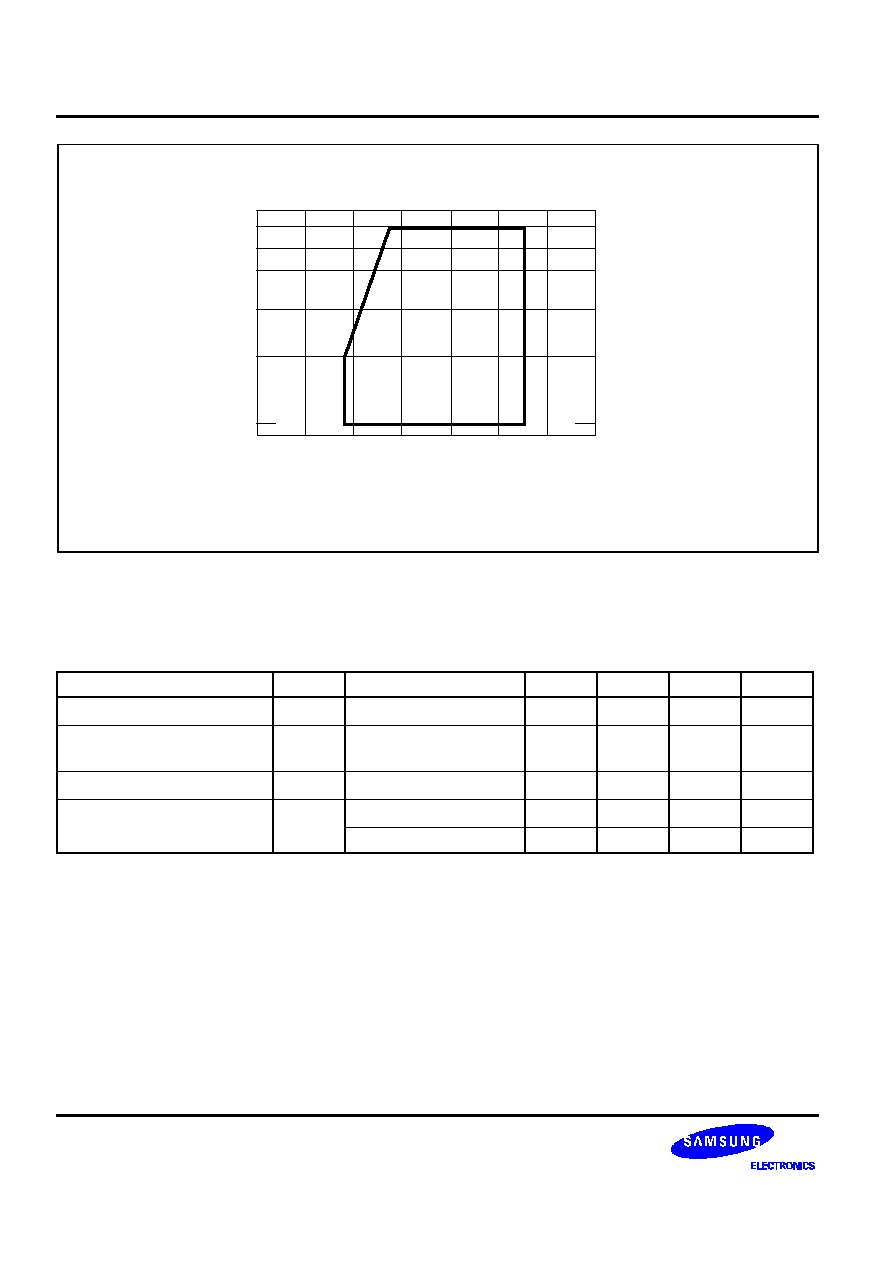
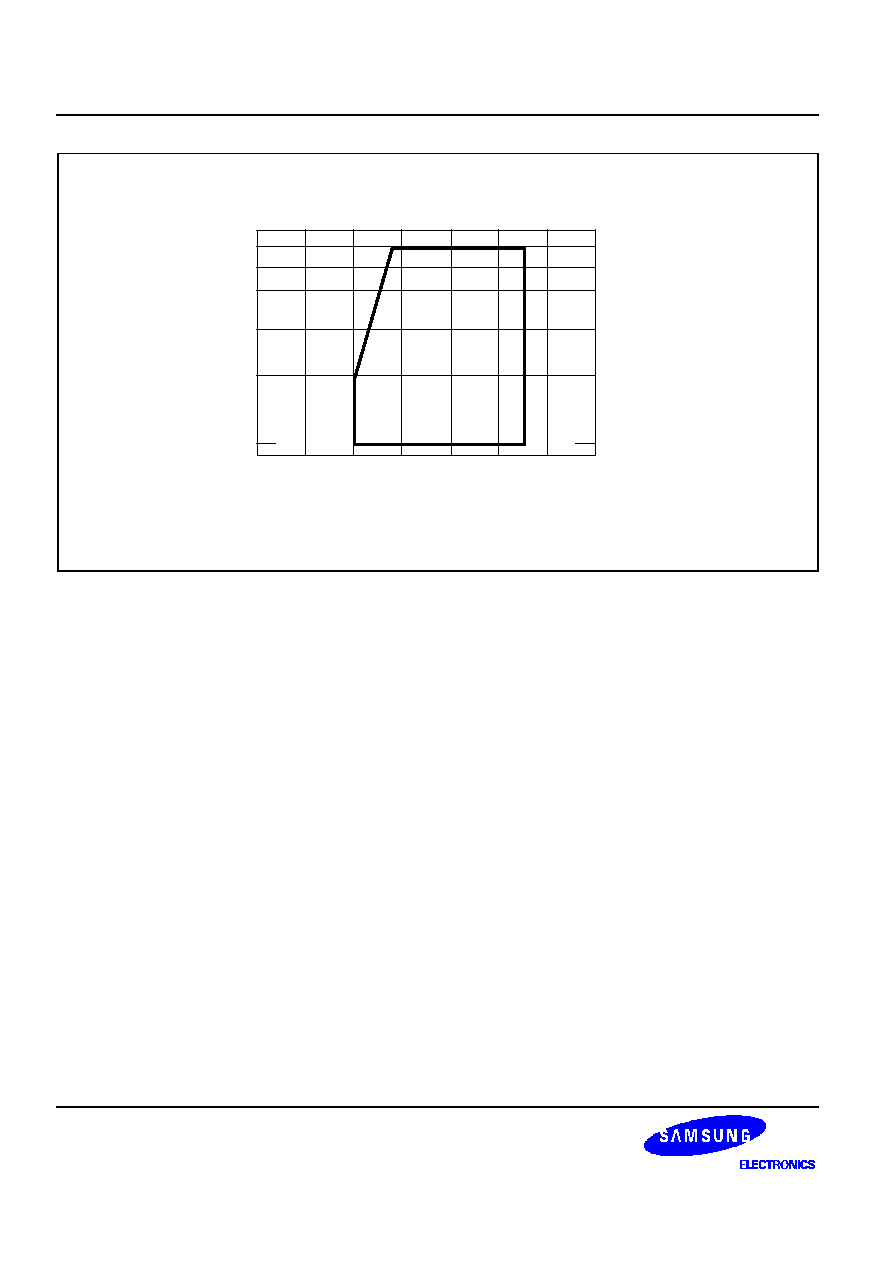
CPU CLOCK = 1/n x oscillator frequency (n = 4, 8, 64)
1 2 3 4 5 6 7
SUPPLY VOLTAGE (V)
1.05 kHz
1.5 MHz
15.625 kHz
CPU CLOCK
4.2 MHz
6 MHz
400 kHz
Main Osc. Freq. ( Divided by 4 )
Figure 131. Standard Operating Voltage Range
Table 136. RAM Data Retention Supply Voltage in Stop Mode
(T
A
= 40
°
C to + 85
°
C)
Parameter
Symbol
Conditions
Min
Typ
Max
Unit
Data retention supply voltage
V
DDDR
1.5
5.5
V
Data retention supply current
I
DDDR
V
DDDR
= 1.5 V
0.1
10
µ
A
Release signal set time
t
SREL
0
µ
s
Oscillator stabilization wait
t
WAIT
Released by
RESET
2
17
/ fx
ms
time
(1)
Released by interrupt
(2)
ms
NOTES
1.
During oscillator stabilization wait time, all CPU operations must be stopped to avoid instability during oscillator start-up.
2.
Use the basic timer mode register (BMOD) interval timer to delay execution of CPU instructions during the wait time.
KS57C0404/C0408/P0408 MICROCONTROLLER
ELECTRICAL DATA
139
TIMING WAVEFORMS
t
SREL
t
WAIT
V
DD
RESET
EXECUTION OF
STOP INSTRUCTION
V
DDDR
DATA RETENTION MODE
STOP MODE
INTERNAL RESET
OPERATION
IDLE MODE
OPERATING
MODE
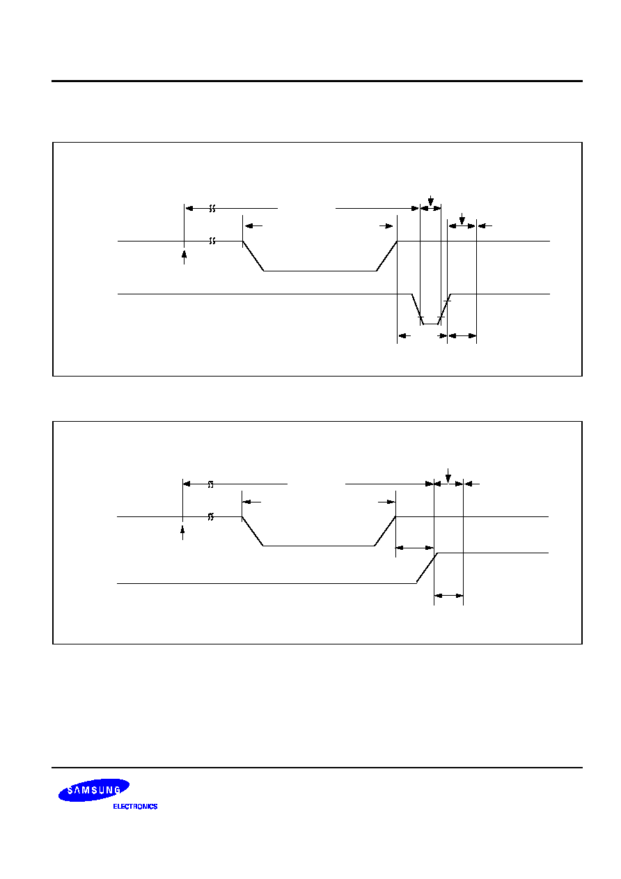
Figure 132. Stop Mode Release Timing When Initiated By
RESET
V
DD
EXECUTION OF
STOP INSTRUCTION
V
DDDR
DATA RETENTION MODE
STOP MODE
t
WAIT
t
SREL
IDLE MODE
NORMAL
OPERATING
MODE
POWER-DOWN MODE TERMINATING SIGNAL
(INTERRUPT REQUEST)
Figure 133. Stop Mode Release Timing When Initiated By Interrupt Request
ELECTRICAL DATA KS57C0404/C0408/P0408 MICROCONTROLLER
1310
Timing Waveforms (continued)
0.8
V
DD
0.2
V
DD
0.8
V
DD
0.2
V
DD
MEASUREMENT
POINTS
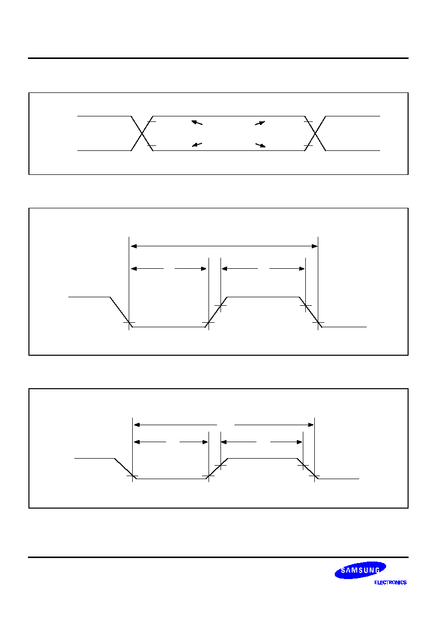
Figure 134. A.C. Timing Measurement Points (Except for X
in
)
Xin
t
XL
t
XH
1 / fx
V
DD
- 0.1 V
0.1 V
Figure 135. Clock Timing Measurement at X
in
TCL
t
TIL
t
TIH
1 /
f
TI
0.8
V
DD
0.2
V
DD
Figure 136. TCL Timing
KS57C0404/C0408/P0408 MICROCONTROLLER
ELECTRICAL DATA
1311
RESET
tRSL
0.2 V DD
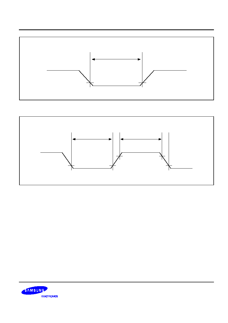
Figure 137. Input Timing for
RESET
Signal
INT0, 1, 2, 4
KS0 to KS7
t
INTL
tINTH
0.8 VDD
0.2 VDD
Figure 138. Input Timing for External Interrupts and Quasi-Interrupts
ELECTRICAL DATA
KS57C0404/C0408/P0408 MICROCONTROLLER
1312
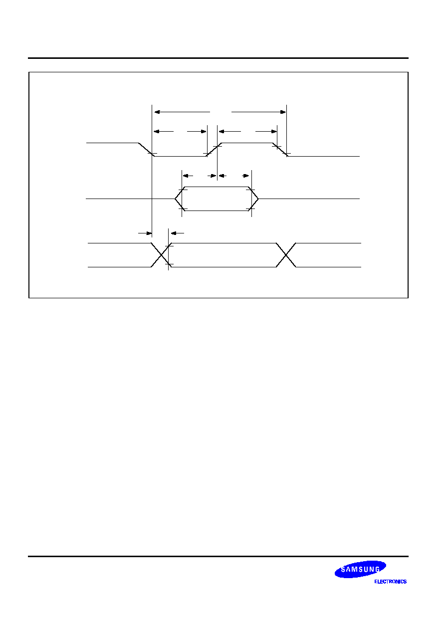
SCK
tKL
tKH
tKCY
0.8 VDD
INPUT DATA
OUTPUT DATA
0.2 VDD
0.8 VDD
0.2 VDD
SI
SO
tKSO
tSIK
tKSI
Figure 139. Serial Data Transfer Timing
KS57C0408/P0408 MICROCONTROLLER
ECHANICAL DATA
141
14
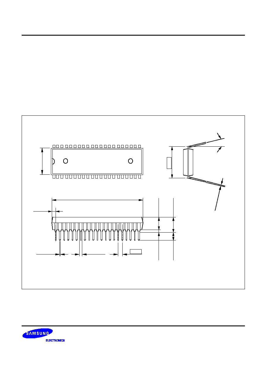
MECHANICAL DATA
This section contains the following information about the device package:
-- 42-SDIP-600 package dimensions in millimeters
-- 44-QFP-1010B package dimensions in millimeters
N OTE: D imens ions are in millim eters.
4 2-SD IP -6 0 0
1
4
.0
0
±
0
.
2
0.50 ± 0. 1
39.10 ± 0.2
0 ~ 15
°
0
.
2
5
+0
.1
0
.
0
5
#1
#21
#42
#22
1
5
.
2
4
(1. 77)
1. 00 ± 0.1
1.778
0
.
5
1
M
I
N
3
.
5
0
±
0
.
2
3
.
3
0
±
0
.
3
5
.
0
8
M
A
X
Figure 141. 42-SDIP-600 Package Dimensions
MECHANICAL DATA
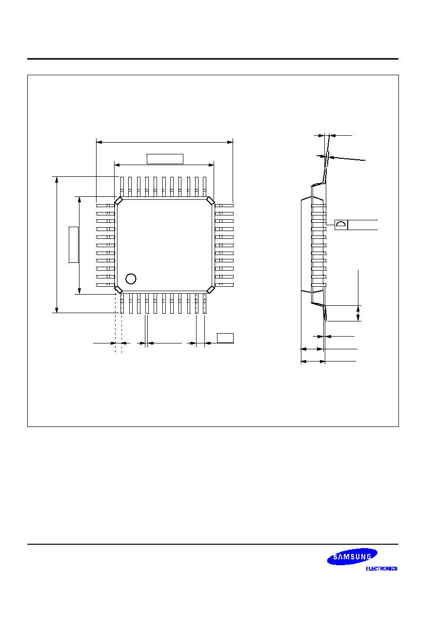
KS57C0408/P0408 MICROCONTROLLER
142
N OTE: Dim ensions are in m illimet ers.
4 4-QFP -1 0 10 B
1
3
.
2
0
±
0
.
3
0
1
0
.
0
0
±
0
.
2
#44
13.20 ± 0.30
10. 00 ± 0.2
#1
0.80
0
.
8
0
±
0
.
2
0
0.15
+ 0.1
0.05
0.1 MAX
0.0 MIN
2.05 ± 0. 1
2.30 MAX
0~8
°
0. 35
+ 0.10
- 0.05
1. 00
Figure 142. 44-QFP-1010B Package Dimensions
KS57C0404/C0408/P0408 MICROCONTROLLER
KS57P0408 OTP
15-1
15
KS57P0408 OTP
OVERVIEW
The KS57P0408 single-chip CMOS microcontroller is the OTP (One Time Programmable)
version of the
KS57C0404/C0408 microcontroller. It has an on-chip OTP ROM instead of masked ROM. The EPROM is
accessed by serial data format.
The KS57P0408 is fully compatible with the KS57C0404/C0408, both in function and in pin configuration.
Because of its simple programming requirements, the KS57P0408 is ideal for use as an evaluation chip for the
KS57C0404/C0408.
VSS / VSS
P7.0 / KS4
P7.1 / KS5
P7.2 / KS6
P7.3 / KS7
P6.0 / KS0
P6.1 / KS1
P6.2 / KS2
P6.3 / KS3
Xin
Xout
RESET /
RESET
P5.0
P5.1
P5.2
P5.3
P4.0
P4.1
P4.2
P4.3
TEST / TEST
42
41
40
39
38
37
36
35
34
33
32
31
30
29
28
27
26
25
24
23
22
1
2
3
4
5
6
7
8
9
10
11
12
13
14
15
16
17
18
19
20
21
P1.3 / INT4
P1.2 / INT2
P1.1 / INT1
P1.0 / INT0
P2.3 / BUZ
P2.2 / CLO
P2.1 / TCLO1
P2.0 / TCLO0
P0.3 / BTCO
P0.2 / SI
P0.1 / SO
P0.0 /
SCK
P8.3
P8.2
P8.1
P8.0
P3.3
P3.2
SDAT / P3.1 / TCL1
SCLK / P3.0 / TCL0
VDD / VDD
KS57P0408
(42-SDIP-600)
NOTE: The bolds indicate an OTP pin name.
Figure 151. KS57P0408 Pin Assignments (42-SDIP Package)
KS57P0408 OTP
KS57C0404/C0408/P0408 MICROCONTROLLER
15-2
NC
P8.0
P8.1
P8.2
P8.3
P0.0 /
SCK
P0.1 / SO
P0.2 / SI
P0.3 / BTCO
P2.0 / TCLO0
P2.1 / TCLO1
P2.2 / CLO
P2.3 / BUZ
P1.0 / INT0
P1.1 / INT1
P1.2 / INT2
P1.3 / INT4
VSS / VSS
P7.0 / KS4
P7.1 / KS5
P7.2 / KS6
P7.3 / KS7
34
35
36
37
38
39
40
41
42
43
44
22
21
20
19
18
17
16
15
14
13
12
NC
P3.3
P3.2
SDAT / P3.1 / TCL1
SCLK / P3.0 / TCL0
VDD / VDD
TEST / TEST
P4.3
P4.2
P4.1
P4.0
KS57P0408
(44-QFP-1010B)
1
2
3
4
5
6
7
8
9
10
11
33
32
31
30
29
28
27
26
25
24
23
P5.3
P5.2
P5.1
P5.0
RESET
/RESET
Xout
Xin
P6.3/KS3
P6.2/KS2
P6.1/KS1
P6.0/KS0
NOTE: The bolds indicate an OTP pin name.
Figure 152. KS57P0408 Pin Assignments (44-QFP Package)
KS57C0404/C0408/P0408 MICROCONTROLLER
KS57P0408 OTP
15-3
Table 151. Descriptions of Pins Used to Read/Write the EPROM
Main Chip
During Programming
Pin Name
Pin Name
Pin No.
I/O
Function
P3.1
SDAT
19 (37)
I/O
Serial data pin. Output port when reading and
input port when writing. Can be assigned as a
Input / push-pull output port.
P3.0
SCLK
20 (38)
I/O
Serial clock pin. Input only pin.
TEST
V
PP
(TEST)
22 (40)
I
Power supply pin for EPROM cell writing
(indicates that OTP enters into the writing
mode). When 12.5 V is applied, OTP is in
writing mode and when 5 V is applied, OTP is in
reading mode. (Option)
RESET
RESET
31 (5)
I
Chip initialization
V
DD
/ V
SS
V
DD
/ V
SS
21/42(39/16)
I
Logic power supply pin. VDD should be tied to
+5 V during programming.
NOTE: ( ) means the 44-QFP OTP pin number.
Table 152. Comparison of KS57P0408 and KS57C0404/C0408 Features
Characteristic
KS57P0408
KS57C0404/C0408
Program Memory
8 K-byte EPROM
4 K-byte mask ROM: KS57C0404
8 K-byte mask ROM: KS57C0408
Operating Voltage (V
DD
)
2.0 V to 5.5 V
1.8 V to 5.5V
OTP Programming Mode
V
DD
= 5 V, V
PP
(TEST)=12.5V
Pin Configuration
42SDIP, 44QFP
42SDIP, 44QFP
EPROM Programmability
User Program 1 time
Programmed at the factory
OPERATING MODE CHARACTERISTICS
When 12.5 V is supplied to the VPP(TEST) pin of the KS57P0408, the EPROM programming mode is entered.
The operating mode (read, write, or read protection) is selected according to the input signals to the pins listed in
Table 153 below.
Table 153. Operating Mode Selection Criteria
VDD
Vpp
(TEST)
REG/
MEM
Address
(A15-A0)
R/W
Mode
5 V
5 V
0
0000H
1
EPROM read
12.5 V
0
0000H
0
EPROM program
12.5 V
0
0000H
1
EPROM verify
12.5 V
1
0E3FH
0
EPROM read protection
NOTE: "0" means Low level; "1" means High level.
KS57P0408 OTP
KS57C0404/C0408/P0408 MICROCONTROLLER
15-4
Table 154. D.C. Electrical Characteristics
(T
A
= 40
°
C to + 85
°
C, V
DD
= 2.0 V to 5.5 V)
Parameter
Symbol
Conditions
Min
Typ
Max
Units
Input High
Voltage
V
IH1
All input pins except those
specified below for V
IH2
V
IH4
0.7 V
DD
V
DD
V
V
IH2
Ports 0, 1, 3, 6, 7, and
RESET
0.8 V
DD
V
IH3
Ports 4 and 5 with pull-up
resistors assigned
0.7 V
DD
Ports 4 and 5 are open-drain
V
IH4
X
in
and X
out
V
DD
0.1
Input Low
Voltage
V
IL1
All input pins except those
specified below for V
IL2
V
IL3
0.3 V
DD
V
V
IL2
Ports 0, 1, 3, 6, 7, and
RESET
0.2 V
DD
V
IL3
X
in
and X
out
0.1
Output High
Voltage
V
OH
I
OH
= 1 mA
Ports except 1, 4, and 5
V
DD
1.0
V
Output Low
Voltage
V
OL1
V
DD
= 4.5 V to 5.5 V
I
OL
= 15 mA, Ports 4, 5 only
2
V
V
DD
= 2.0 to 5.5 V
I
OL
= 1.6mA
0.4
V
OL2
V
DD
= 4.5 V to 5.5 V
I
OL
= 4 mA
All output ports except ports 4,5
2
V
DD
= 2.0 to 5.5 V
I
OL
= 1.6mA
0.4
Input High
Leakage
Current
I
LIH1
V
I
= V
DD
All input pins except those
specified below for I
LIH2
3
µA
I
LIH2
V
I
= V
DD
X
in
and X
out
20
Input Low
Leakage
Current
I
LIL1
V
I
= 0
V
All input pins except below and
RESET
3
µA
I
LIL2
V
I
= 0 V
X
i
n
and X
out
only
20
KS57C0404/C0408/P0408 MICROCONTROLLER
KS57P0408 OTP
15-5
Table 154. D.C. Electrical Characteristics (Continued)
(T
A
= 40
°
C to + 85
°
C, V
DD
= 2.0 V to 5.5 V)
Parameter
Symbol
Conditions
Min
Typ
Max
Units
Output High
Leakage Current
I
LOH
V
O
= V
DD,
All output pins
3
µA
Output Low
Leakage Current
I
LOL
V
O
= 0 V, All output pins
3
µA
Pull-Up
Resistor
R
L1
V
I
= 0 V; V
DD
= 5 V
Ports 0, 1 (not P1.3), 2, 3, 6, 7
25
47
100
k
V
DD
= 3 V
50
95
200
R
L2
V
O
= V
DD
2V; V
DD
= 5V
Ports 4 and 5 only
15
47
70
V
DD
= 3 V
10
45
60
R
L3
V
DD
= 5 V; V
I
= 0V;
RESET
100
220
400
V
DD
= 3 V
200
450
800
Pull-Down
R
L4
V
DD
= 5 V; V
I
= V
DD
; Port 8
25
47
100
k
Resistor
V
DD
= 3 V
50
95
200
Supply
I
DD1
Run mode; V
DD
= 5 V
±
10%
6.0 MHz
3.9
8.0
mA
Current
(1)
Crystal oscillator; C1 = C2 = 22 pF
4.19 MHz
2.9
5.5
V
DD
= 3 V ± 10%
6.0 MHz
1.8
4.0
4.19 MHz
1.3
3.0
I
DD2
Run mode; V
DD
= 5 V
±
10%
6.0 MHz
1.3
2.5
mA
crystal oscillator, C1 = C2 = 22 pF
4.19 MHz
1.2
1.8
V
DD
= 3 V ± 10%
6.0 MHz
0.5
1.5
4.19 MHz
0.44
1.0
I
DD
3
Stop mode; V
DD
= 5 V
±
10%
0.2
3
µA
Stop mode; V
DD
= 3 V
±
10%
0.1
2
NOTES
1.
D.C. electrical values for Supply Current (I
DD1
to I
DD3
) do not include current drawn through internal pull-up resistors.
2.
The supply current assumes a CPU clock of fx/4.
KS57P0408 OTP
KS57C0404/C0408/P0408 MICROCONTROLLER
15-6
Table 155. A.C. Electrical Characteristics
(T
A
= 40
°
C to + 85
°
C, V
DD
= 2.0 V to 5.5 V)
Parameter
Symbol
Conditions
Min
Typ
Max
Units
Instruction Cycle
Time
t
CY
V
DD
= 2.7 V to 5.5 V
0.67
64
µs
V
DD
= 2.0 V to 5.5 V
0.95
TCL0, TCL1 Input
Frequency
f
TI0
,
f
TI1
V
DD
= 2.7 V to 5.5 V
0
1.5
MHz
V
DD
= 2.0 V to 5.5V
1
TCL0, TCL1 Input
High, Low Width
t
TIH0
,
t
TIL0
t
TIH1
,
t
TIL1
V
DD
= 2.7 V to 5.5 V
0.48
µs
V
DD
= 2.0 V to 5.5 V
1.8
SCK
Cycle Time
t
KCY
V
DD
= 2.7 V to 5.5 V
External
SCK
source
800
µs
Internal
SCK
source
670
V
DD
= 2.0 V to 5.5 V
External
SCK
source
3200
Internal
SCK
source
3800
SCK
High, Low
Width
t
KH,
t
KL
V
DD
= 2.7 V to 5.5 V
External
SCK
source
335
µs
Internal
SCK
source
t
KCY
/
2 50
V
DD
= 2.0 V to 5.5 V
External
SCK
source
1600
Internal
SCK
source
t
KCY
/
2 150
KS57C0404/C0408/P0408 MICROCONTROLLER
KS57P0408 OTP
15-7
Table 155. A.C. Electrical Characteristics (Continued)
(T
A
= 40
°
C to + 85
°
C, V
DD
= 2.0 V to 5.5 V)
Parameter
Symbol
Conditions
Min
Typ
Max
Units
SI Setup Time to
SCK
High
t
SIK
V
DD
= 2.7 V to 5.5 V
External
SCK
source
100
ns
Internal
SCK
source
150
V
DD
= 2.0 V to 5.5 V
External
SCK
source
150
Internal
SCK
source
500
SI Hold Time to
SCK
High
t
KSI
V
DD
= 2.7 V to 5.5 V
External
SCK
source
400
ns
Internal
SCK
source
400
V
DD
= 2.0 V to 5.5 V
External
SCK
source
600
Internal
SCK
source
500
Output Delay for
SCK
to SO
t
KSO
(1)
V
DD
= 2.7 V to 5.5 V
External
SCK
source
300
ns
Internal
SCK
source
250
V
DD
= 2.0 V to 5.5 V
External
SCK
source
1000
Internal
SCK
source
1000
Interrupt Input
High, Low Width
t
INTH
, t
INTL
INT0
(2)
µ
s
INT1, INT2, INT4, KS0 - KS7
10
RESET
Input Low
Width
t
RSL
Input
10
µ
s
NOTES
1.
R(1Kohm) and C(100pF) are the load resistance and load capacitance of the SO output line.
2.
Minimum value for INT0 is based on a clock of 2t
CY
or 128 / fx as assigned by the IMOD0 register setting.
KS57P0408 OTP
KS57C0404/C0408/P0408 MICROCONTROLLER
15-8
CPU CLOCK = 1/n x oscillator frequency (n = 4, 8, 64)
SUPPLY VOLTAGE (V)
1.05 kHz
1.5 MHz
15.625 kHz
CPU CLOCK
4.2 MHz
6 MHz
400 kHz
Main Osc. Freq. ( Divided by 4 )
1
2
3
4
5
6
7
Figure 153. Standard Operating Voltage Range
KS57C0404/C0408/P0408 MICROCONTROLLER
KS57P0408 OTP
15-9
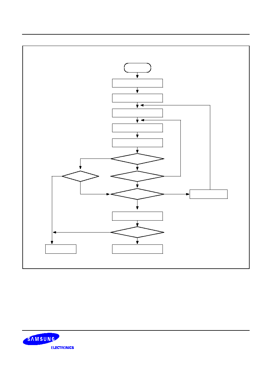
START
Address= First Location
V
DD
=5V, V
PP
=12.5V
x = 0
Program One 1ms Pulse
Increment X
x = 10
Verify 1 Byte
Last Address
V
DD
= V
PP
= 5 V
Compare All Byte
Device Passed
Increment Address
Verify Byte
Device Failed
PASS
FAIL
NO
FAIL
YES
FAIL
NO
Figure 154. OTP Programming Algorithm

KS57P0408 OTP
KS57C0404/C0408/P0408 MICROCONTROLLER
15-10
NOTES