
ü
11-53
11
T
R
A
N
S
C
EI
VE
R
S
Product Description
Ordering Information
Typical Applications
Features
Functional Block Diagram
RF Micro Devices, Inc.
7628 Thorndike Road
Greensboro, NC 27409, USA
Tel (336) 664 1233
Fax (336) 664 0454
http://www.rfmd.com
Optimum Technology Matching® Applied
Si BJT
GaAs MESFET
GaAs HBT
Si Bi-CMOS
SiGe HBT
Si CMOS
17
18
26
12
11
9
Linear
RSSI
24
7
5
Gain
Control
47
3
31
30
34
Prescaler
128/129 or
64/65
Phase
Detector &
Charge Pump
41
40
39
38
35
36
Lock
Detector
42
43
Ref
Select
37
14
13
DATA OUT
RSSI
DIV CTRL
MOD CTRL
OSC SEL
23
MU
T
E
IF
2
I
N
IF
1
O
U
T
21
I
F
2
BP+
20
VREF
I
F
22
I
F
2
BP-
16
I
F
1
BP-
15
I
F
1
BP+
IF
1
I
N
-
IF
1
I
N
+
MIX OUT-
MIX OUT+
MIX IN
LNA OUT
RX IN
TX OUT
LV
L
A
D
J
RESNTR+
MOD
I
N
VREF
P
L
O
CK
DET
L
OOP
F
L
T
OS
C
B
1
OS
C
B
2
OS
C
E
45 PRESCL OUT
28
IF
2
O
U
T
27
DEM
O
D
I
N
RESNTR-
25 FM OUT
RF2905
433/868/915MHZ FM/FSK/ASK/OOK
TRANSCEIVER
· Wireless Meter Reading
· Keyless Entry Systems
· 433/868/915MHz ISM Band Systems
· Wireless Data Transceiver
· Wireless Security Systems
· Battery Powered Portable Devices
The RF2905 is a monolithic integrated circuit intended for
use as a low cost FM transceiver. The device is provided
in 7 mmx7mm, 48-lead plastic LQFP packaging and is
designed to provide a fully functional FM transceiver. The
chip is intended for linear (AM, FM) or digital (ASK, FSK,
OOK) applications in the North American 915MHz ISM
band and European 433MHz and 868MHz ISM bands.
The integrated VCO, dual modulus/dual divide (128/129
or 64/65) prescaler, and reference oscillator require only
the addition of an external crystal to provide a complete
phase-locked oscillator.
· Fully Monolithic Integrated Transceiver
· 2.7V to 5.0V Supply Voltage
· Narrow Band and Wide Band FM/FSK
· 300MHz to 1000MHz Frequency Range
· 10dB Cascaded Noise Figure
· 10mW Output Power at 433MHz
RF2905
433/868/915MHz FM/FSK/ASK/OOK Transceiver
RF2905 PCBA-L
Fully Assembled Evaluation Board (433MHz)
RF2905 PCBA-M Fully Assembled Evaluation Board (868MHz)
RF2905 PCBA-H Fully Assembled Evaluation Board (915MHz)
11
Rev B11 010516
Dimensions in mm.
7.00
+ 0.10 sq.
9.00
+ 0.20 sq.
0.22
+ 0.05
7° MAX
0° MIN
0.60
0.15
0.10
+
0.127
1.40
+ 0.05
0.50
0.35
0.25
Package Style: LQFP-48, 7x7

11-54
RF2905
Rev B11 010516
11
T
R
A
N
S
C
EI
VE
R
S
Absolute Maximum Ratings
Parameter
Ratings
Unit
Supply Voltage
-0.5 to +5.5
V
DC
Control Voltages
-0.5 to +5.0
V
DC
Input RF Level
+10
dBm
Output Load VSWR
50:1
Operating Ambient Temperature
-40 to +85
°C
Storage Temperature
-40 to +150
°C
Parameter
Specification
Unit
Condition
Min.
Typ.
Max.
Overall
T=25 °C, V
CC
= 3.6V, Freq= 915MHz
RF Frequency Range
300 to 1000
MHz
VCO and PLL Section
VCO Frequency Range
300 to 1000
MHz
Prescaler divide ratio
64/65 or 128/129
Prescaler Output Impedance
50
PLL Phase Noise
-75
dBc/Hz
Freq= 915MHz, 10kHz Offset, 5kHz Loop
Bandwidth
-100
dBc/Hz
Freq= 915MHz, 100kHz Offset, 5kHz loop
Bandwidth
Reference Frequency
TBD
17
MHz
Crystal R
S
50
100
Charge Pump Current
-40
+40
µ
A
Transmit Section
Max Modulation Frequency
2
MHz
Min Modulation Frequency
Set by loop filter bandwidth
Maximum Power Level
+7
+10
dBm
Freq= 433MHz
0
+3
8
dBm
Freq= 915MHz
Power Control Range
12
dB
Power Control Sensitivity
10
dB/V
Max FM Deviation
200
kHz
Instantaneous frequency deviation is
inversely proportional with the modulation
voltage
Antenna Port Impedance
50
TX ENABL= "1". RX ENABL= "0"
Antenna Port VSWR
1.5:1
TX Mode
Modulation Input Impedance
4
k
Harmonics
-23
dBc
Spurious
dBc
Compliant to Part 15.249 and I-ETS 300 220
Overall Receive Section
Frequency Range
300 to 1000
MHz
Cascaded Voltage Gain
35
dB
Freq= 433MHz
23
dB
Freq= 915MHz
Cascaded Noise Figure
10
dB
Cascaded Input IP
3
-31
dBm
Freq= 433MHz
-26
dBm
Freq= 915MHz
RX Sensitivity
-95
-101
dBm
IF BW = 180kHz, Freq= 915MHz, S/N= 8dB
LO Leakage
-70
dBm
RSSI DC Output Range
0.5 to 2.5
V
R
LOAD
=51k
RSSI Sensitivity
25
mV/dB
RSSI Dynamic Range
70
80
dB
Caution! ESD sensitive device.
RF Micro Devices believes the furnished information is correct and accurate
at the time of this printing. However, RF Micro Devices reserves the right to
make changes to its products without notice. RF Micro Devices does not
assume responsibility for the use of the described product(s).

11-55
RF2905
Rev B11 010516
11
T
R
A
N
S
C
EI
VE
R
S
Parameter
Specification
Unit
Condition
Min.
Typ.
Max.
LNA
Voltage Gain
23
dB
433MHz
16
dB
915MHz
Noise Figure
4.8
dB
433MHz
5.5
dB
915MHz
Input IP
3
-27
dBm
433MHz
-20
dBm
915MHz
Input P
1dB
-37
dBm
433MHz
-30
dBm
915MHz
Antenna Port Impedance
50
RX ENABL= "1". TX ENABL= "0"
Antenna Port VSWR
1.5:1
RX Mode
Output Impedance
Open Collector
433MHz
Open Collector
915MHz
Mixer
Single-ended configuration
Conversion Voltage Gain
8
dB
433MHz
7
dB
915MHz
Noise Figure (SSB)
10
dB
433MHz
17
dB
915MHz
Input IP
3
-21
dBm
433MHz
-17
dBm
915MHz
Input P
1dB
-31
dBm
433MHz
-28
dBm
915MHz
Maximum Output Voltage
V
PP
Balanced
First IF Section
IF Frequency Range
0.1
10.7
25
MHz
Voltage Gain
34
dB
IF= 10.7MHz, Z
L
= 330
Noise Figure
13
dB
IF1 Input Impedance
330
IF1 Output Impedance
330
Second IF Section
IF Frequency Range
0.1
10.7
25
MHz
Voltage Gain
60
dB
IF= 10.7MHz
IF2 Input Impedance
330
IF2 Output Impedance
1
k
At IF2 OUT- pin
Demod Input Impedance
10
k
FM Output Impedance
500
Data Output Impedance
>1
FM Output Bandwidth
500
kHz
3dB Bandwidth, Dependent upon IF band-
width and Discriminator.
Data Output Bandwidth
500
kHz
3dB Bandwidth, Z
LOAD
=1M
|| 3pF; Depen-
dent upon IF bandwidth and Discriminator.
Data Output Level
0.3
V
CC
-0.3
V
Z
LOAD
=1M
|| 3pF; Output voltage is pro-
portional with the instantaneous frequency
deviation.
FM Output DC Level
2.6
V
Z
LOAD
>10k
FM Output AC Level
200
mV
PP
Z
LOAD
>10k

11-56
RF2905
Rev B11 010516
11
T
R
A
N
S
C
EI
VE
R
S
Parameter
Specification
Unit
Condition
Min.
Typ.
Max.
Power Down Control
Logical Controls "ON"
2.0
V
Voltage supplied to the input
Logical Controls "OFF"
1.0
V
Voltage supplied to the input
Control Input Impedance
25k
Turn On Time
4
ms
Reference Crystal= 7.075MHz
Turn Off Time
4
ms
Dependent upon reference crystal. Higher
RX to TX and TX to RX Time
4
ms
frequencies reduce turn on/off times
Power Supply
Voltage
3.6
V
Specifications
2.7 to 5.0
V
Operating limits
Current Consumption
22
25
34.5
mA
TX Mode, LVL ADJ= 3.6V
8
10
13.5
mA
TX Mode, LVL ADJ= 0V
7
9
12
mA
RX Mode
1
µ
A
Power Down Mode which sets:
PLL ENABL, TX ENABL, RX ENABL,
LVL ADJ, OSC SEL, and MUTE = 0V
5.3
8
10
mA
PLL Only Mode

11-57
RF2905
Rev B11 010516
11
T
R
A
N
S
C
EI
VE
R
S
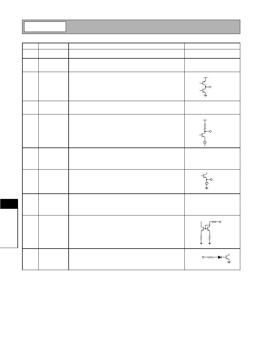
Pin
Function
Description
Interface Schematic
1
RX ENABL
Enable pin for the receiver circuits. RX ENABL> 2.0V powers up all
receiver functions. RX ENABL<1.0V turns off all receiver functions
except the PLL functions and the RF mixer.
2
TX ENABL
Enables the transmitter circuits. TX ENABL>2.0V powers up all trans-
mitter functions. TX ENABL<1.0V turns off all transmitter functions
except the PLL functions.
3
TX OUT
RF output pin for the transmitter electronics. TX OUT output impedance
is a low impedance when the transmitter is enabled. TX OUT is a high
impedance when the transmitter is disabled.
4
GND2
Ground connection for the 40dB IF limiting amplifier and Tx PA func-
tions. Keep traces physically short and connect immediately to ground
plane for best performance.
5
RX IN
RF input pin for the receiver electronics. RX IN input impedance is a
low impedance when the transmitter is enabled. RX IN is a high imped-
ance when the receiver is disabled.
6
GND1
Ground connection for RF receiver functions. Keep traces physically
short and connect immediately to ground plane for best performance.
7
LNA OUT
Output pin for the receiver RF low noise amplifier. This pin is an open
collector output and requires an external pull up coil to provide bias and
tune the LNA output.
8
GND3
Same as pin 4.
9
MIX IN
RF input to the RF Mixer. An LC matching network between LNA OUT
and MIX IN can be used to connect the LNA output to the RF mixer
input in applications where an image filter is not needed or desired.
10
GND5
GND5 is the ground connection shared by the input stage of the trans-
mit power amplifier and the receiver RF mixer.
11
MIX OUT+
Complementary (with respect to pin 12) IF output from the RF mixer.
Interfaces directly to 10.7MHz ceramic IF filters as shown in the appli-
cation schematic. A pull-up inductor and series matching capacitor
should be used to present a 330
termination impedance to the
ceramic filter. Alternately, an IF tank can be used to tailor the IF fre-
quency and bandwidth to meet the needs of a given application.
12
MIX OUT-
IF output from the RF mixer. For a balanced mixer output, pull-up induc-
tors from pin 11 and 12 to V
CC
and a capacitor between the pins should
be used. The sum of the total pull-up inductance should be used to res-
onate the capacitor between pins 11 and 12. DC blocking capacitors of
10nF can then be used to connect the balanced output to IF1 IN+ (pin
13) and IF1 IN- (pin 14).
See pin 11.
50 k
RX ENABL
40 k
20 k
TX ENABL
TX OUT
20
V
CC
RX IN
500
LNA OUT
V
CC
GND5
MIX IN
MIX OUT-
MIX OUT+
15 pF
15 pF
GND5
GND5

11-58
RF2905
Rev B11 010516
11
T
R
A
N
S
C
EI
VE
R
S
Pin
Function
Description
Interface Schematic
13
IF1 IN+
Balanced IF input to the 40dB limiting amplifier strip. A 10nF DC block-
ing capacitor is required on this input.
14
IF1 IN-
Functionally the same as pin 13 except inverting node amplifier input.
In single-ended applications, this input should be bypassed directly to
ground through a 10nF capacitor.
See pin 13.
15
IF1 BP+
DC feedback node for the 40dB limiting amplifier strip. A 10nF bypass
capacitor from this pin to ground is required.
See pin 13.
16
IF1 BP-
Same as pin 15.
See pin 13.
17
IF1 OUT
IF output from the 40dB limiting amplifier. The IF1 OUT output presents
a nominal 330
output resistance and interfaces directly to 10.7MHz
ceramic filters.
18
IF2 IN
Balanced IF input to the 60dB limiting amplifier strip. A 10nF DC block-
ing capacitor is required on this input. The IF2 IN input presents a nom-
inal 330
input resistance and interfaces directly to 10.7MHz ceramic
filters.
19
GND6
Ground connection for 60dB IF limiting amplifier. Keep traces physically
short and connect immediately to ground plane for best performance.
20
VREF IF
DC voltage reference for the IF limiting amplifiers. A 10nF capacitor
from this pin to ground is required.
21
IF2 BP+
DC feedback node for the 60dB limiting amplifier strip. A 10nF bypass
capacitor from this pin to ground is required.
See pin 18.
22
IF2 BP-
Same as pin 21.
See pin 18.
23
MUTE
This pin is used to mute the data output (DATA OUT). MUTE > 2.0V
turns the DATA OUT signal on. MUTE <1.0V turns the DATA OUT sig-
nal off. The MUTE signal should be logic low in the Sleep Mode.
24
RSSI
A DC voltage proportional to the received signal strength is output from
this pin. The output voltage range is 0.5V to 2.5V, into 51k
load, and
increases with increasing signal strength.
25
FM OUT
Linear output from the FM demodulator. This pin is used in analog
applications when signal fidelity is important. This output is inverted for
low side injection of the LO and normal for high side injection.
26
DATA OUT
Demodulated data output from the demodulator. Output levels on this
are TTL/CMOS compatible. The magnitude of the load impedance is
intended to be 1M
or greater. When using a RF2905 transmitter and
receiver back to back a data inversion will occur, when the LO is low
side injected. A high side injection will add an inversion of the Rx data.
IF1 IN-
IF1 IN+
330
330
60 k
60 k
IF1 BP+
IF1 BP-
IF1 OUT
IF2 IN
330
330
60 k
60 k
IF2 BP+
IF2 BP-
25 k
75 k
MUTE
V
CC
RSSI
FM OUT
DATA OUT

11-59
RF2905
Rev B11 010516
11
T
R
A
N
S
C
EI
VE
R
S
Pin
Function
Description
Interface Schematic
27
DEMOD IN
This pin is the input to the FM demodulator. This pin is NOT AC cou-
pled. Therefore, a DC blocking capacitor is required on this pin to avoid
shorting the demodulator input with the LC tank. A ceramic discrimina-
tor or DC blocked LC tank resonant at the IF should be connected to
this pin.
28
IF2 OUT
Balanced IF output from the 60dB limiting amplifier strip. This pin is
intended to be connected to pin 27 through a 4pF (suggested) capaci-
tor and an FM discriminator circuit.
29
VCC6
This pin is used is supply DC bias to the second IF amplifier, Demodu-
lator and Data Slicer. An IF bypass capacitor should be connected
directly to this pin and returned to ground. A 10nF capacitor is recom-
mended for 10.7MHz IF applications.
30
RESNTR+
This port is used to supply DC voltage to the VCO as well as to tune the
center frequency of the VCO. Equal value inductors should be con-
nected to this pin and pin 31 although a small imbalance can be used
to tune in the proper frequency range.
31
RESNTR-
See RESNTR+ description.
See pin 30.
32
VCC2
This pin is used is supply DC bias to the VCO, prescaler, and PLL. An
RF bypass capacitor should be connected directly to this pin and
returned to ground. A 22pF capacitor is recommended for 915MHz
applications. A 68pF capacitor is recommended for 433MHz applica-
tions.
33
GND4
GND4 is the ground shared on chip by the VCO, prescaler, and PLL
electronics.
34
MOD IN
FM analog or digital modulation can be imparted to the VCO through
this pin. The VCO varies in accordance to the voltage level presented
to this pin. To set the deviation to a desired level, a voltage divider refer-
enced to Vcc is the recommended. This deviation is also dependent
upon the overall capacitance of the external resonant circuit.
See pin 30.
35
DIV CTRL
This pin is used to select the desired prescaler divisor. A logic high
(DIVCTRL>2.0V) selects the 64/65 divisor. A logic low
(DIVCTRL<1.0V) selects the 128/129 divisor.
36
MOD CTRL
This pin is used to select the prescaler modulus. A logic high (MOD
CTRL>2.0V) selects 64 or 128 for the prescaler divisor. A logic low
(MOD CTRL<1.0V) selects 65 or 129 for the prescaler divisor.
Due to design timing constraints, the prescaler in the divide by 65 or
129 modes has a limited frequency range for accurate operation.
These two modes are not recommended for use from 400MHz to
460MHz.
37
OSC SEL
A logic high (OSC SEL>2.0V) applied to this pin powers on reference
oscillator 2 and powers down reference oscillator 1. A logic low (OSC
SEL<1.0V) applied to this pin powers on reference oscillator 1 and
powers down reference oscillator 2.
38
OSC B2
This pin is connected directly to the reference oscillator 2 transistor
base. The intended reference oscillator configuration is a modified Col-
pitts.
DEMOD IN
10 k
V
CC
IF2 OUT
RESNTR-
ESNTR+
4 k
MOD IN
DIV CTL
MOD CTL
OSC E
OSC B1
OSC B2
11-60
RF2905
Rev B11 010516
11
T
R
A
N
S
C
EI
VE
R
S
Pin
Function
Description
Interface Schematic
39
OSC E
This pin is connected directly to the emitter of the reference oscillator
transistors.
See pin 38.
40
OSC B1
This pin is connected directly to the reference oscillator 1 transistor
base. The intended reference oscillator configuration is a modified Col-
pitts.
See pin 38.
41
LOOP FLT
Output of the charge pump, and input to the VCO control. An RC net-
work from this pin to ground is used to establish the PLL bandwidth.
42
VREF P
Bypass pin for the prescaler reference voltage. A 33nF capacitor to
ground is needed to suppress reference spurs in the device. This value
may be different for different PCB arrangements.
43
LOCK DET
This pin provides an analog output indicating the lock status of the PLL.
The amplitude of this signal is typically 200mV
PP
around a DC level of
V
CC
-0.1V.
44
VCC1
This pin is used to supply DC bias to the LNA, Mixer, first IF Amp, and
Bandgap reference. A RF bypass capacitor should be connected
directly to this pin and returned to ground. A 22pF capacitor is recom-
mended for 915MHz applications. A 68pF capacitor is recommended
for 433MHz applications.
45
PRESCL
OUT
Dual-modulus/Dual-divide prescaler output. The output can be inter-
faced to an external PLL IC for additional flexibility in frequency pro-
gramming.
46
VCC3
This pin is used to supply DC bias and collector current to the transmit-
ter PA. A RF bypass capacitor should be connected directly to this pin
and returned to ground. A 22pF capacitor is recommended for 915MHz
applications. A 68pF capacitor is recommended for 433MHz applica-
tions.
47
LVL ADJ
This pin is used to vary the transmitter output power. An output level
adjustment range greater than 12dB is provided through analog volt-
age control of this pin. DC current of the transmitter power amp ia also
reduced with output power. This pin MUST be low when the transmitter
is disabled.
48
PLL ENABL
This pin is used to power up or down the VCO and PLL. A logic high
(PLLENABL> 2.0V) powers up the VCO and PLL electronics. A logic
low (PLLENABL<1.0V) powers down the PLL and VCO.
LOOP FLT
V
CC
LOCK DET
20 k
V
CC
PRESCL
OUT
400
4 k
LVL ADJ
40 k
50 k
PLL ENABL

11-61
RF2905
Rev B11 010516
11
T
R
A
N
S
C
EI
VE
R
S
RF2905 Theory of Operation and Application Information
The RF2905 is a part of a family of low-power RF
transceiver IC's that was developed for wireless data
communication devices operating in the European 433/
868MHz ISM bands or 915MHz US ISM band.This IC
has been implemented in a 15GHz silicon bipolar pro-
cess technology that allows low-power transceiver
operation in a variety of commercial wireless products.
In its basic form, the RF2905 can implement a two-way
half duplex FSK transceiver with the addition of some
crystals, filters, and passive components. There are
two reference crystals that allow for the transmit carrier
and the receiver LO to be independently generated
with a common PLL and VCO. The receiver IF section
is optimized to interface with low cost 10.7 MHz
ceramic filters but has a -3 dB bandwidth of 25 MHz
and can still be used (with lower gain) at higher fre-
quency with the other type of filters. The PA output and
LNA input are available on separate pins and are
designed to be connected together through a DC
blocking capacitor. In the Transmit mode, the PA will
have a 50
impedance and the LNA will be a high
impedance. In Receive mode, the LNA will have a 50
interface and the PA will have a high impedance. This
eliminates the need for a TX/RX switch and allows a
single RF filter to be used in transmit and receive
modes. Separate access to the PA and LNA allow the
RF2905 to interface with external components such as
higher power PA's, lower NF LNA's, upconverters, and
downconverters for a variety of implementations.
FM/FSK SYSTEMS
The MOD IN pin drives an internal varactor for modu-
lating the VCO. This pin can be driven with a voltage
level needed to generate the desired deviation. This
voltage can be carried on a DC bias to select the
desired slope (deviation/volt) for FM systems. Or, a
resistor divider network referenced to Vcc or ground
can divide down logic level signals to the appropriate
level for a desired deviation in FSK systems.
On the receiver demod, two outputs are available, an
analog FM output and a digital FSK output. The FM
output is a buffered signal coming off of the quadrature
demodulator. The digital output is generated by a data
slicer that is DC coupled differentially to the demodula-
tor. An on-chip 1.6MHz RC filter is provided at the
demodulator output to filter the undesired 2xIF product.
This balanced data slicer has a speed advantage over
a conventional adaptive data slicer where a large
capacitor is used to provide DC reference for bit deci-
sion. Since the balanced data slicer does not have to
charge a large capacitor, the RF2905 exhibits a very
fast response time. For best operation of the on-chip
data slicer, FM deviation needs to exceed the carrier
frequency error anticipated between the receiver and
transmitter with margin.
The data slicer itself is a transconductance amp and
the DATA OUT pin is capable of driving rail to rail out-
put only into a very high impedance and small capaci-
tance. The amount of capacitance will determine the
bandwidth of the DATA OUT. At a 3pF load, the band-
width is in excess of 500kHz. The rail to rail output of
the data slicer is also limited by the frequency deviation
and bandwidth of the IF filters. With the 180kHz band-
width filters on the eval boards, the rail to rail output is
limited to less than 140kHz. Choosing the right IF
bandwidth and deviation vs. data rate (mod index) is
important in evaluating the applicability of the RF2905
for a given data rate.
While this type of data slicer is best for wideband devi-
ation, it can also work for narrowband if care is taken to
minimize frequency differences. By loading down the
DATA OUT pin, the output will be limited to a small data
signal on a DC carrier. With this signal, an external
data slicer can be used to achieve higher data rates or
improve performance in narrow deviations. Alterna-
tively, an AFC loop can be added to correct for fre-
quency errors with a few external components.
For FM or FSK modulation, an internal varactor is used
to directly modulate the VCO with the baseband data.
The primary consideration when directly modulating
the VCO is the data rate verses PLL loop bandwidth.
The PLL will track out the modulation to the extent of
its loop bandwidth which distorts the modulating data.
Therefore, the lower frequency components of the
modulating data should be 5 to 10 times the loop band-
width to minimize the distortion. The lower frequency
components are generated by long strings of 1's or 0's
in the data stream. By limiting the number of consecu-
tive, same bits, the lower frequency component can be
set. In addition, the data stream should be balanced to
minimize distortion. Using a coding pattern such as
Manchester is highly recommended to optimize system
performance.
The PLL loop bandwidth is important in several other
system parameters. For example, switching from trans-
mit to receive requires the VCO to retune to another
frequency. The switching speed is proportional to the
loop bandwidth, the higher the loop bandwidth, the

11-62
RF2905
Rev B11 010516
11
T
R
A
N
S
C
EI
VE
R
S
faster the switching times. Phase noise of the VCO is
another factor. Phase noise outside of the loop band-
width is due to the noise of the VCO itself rather than
the crystal reference. A design trade-off must be made
here in selecting a PLL loop bandwidth with acceptable
phase noise and switching characteristics and minimal
distortion of the modulation data.
AM/ASK SYSTEMS
The transmitter of the RF2905 has an output power
level adjustment (LVL ADJ) that can be used to provide
approximately 18dB of power control for amplitude
modulation. The RSSI output of the receiver section
can be used to recover the modulation. The RSSI out-
put is from a current source and needs to have a resis-
tor to convert to a voltage. A 51k
resistive load will
produce an RSSI voltage of 0.7V to 2.5V, typically. A
parallel capacitor is suggested to limit the bandwidth
and filter noise. For ASK applications, the 18 dB range
of the LVL ADJ does not produce enough voltage
swing in the RSSI for reliable communication. The On-
Off keying (OOK) is suggested to provide reliable com-
munications. To achieve this, both the LVL ADJ and TX
ENABL need to be controlled together (please note
that LVL ADJ cannot be left high when TX ENABL is
low). This will provide a on/off ratio of >50 dB. One
unfortunate consequence of modulating this way is
VCO pulling by the power amp. This results in a spuri-
ous output outside the desired transmit band as the
PLL momentarily loses lock and reacquires. This can
be avoided by pulse shaping the TX data to slow the
change in the VCO load to a pace that the PLL can
track with its given loop bandwidth. The loop bandwidth
can also be increased to allow it to track faster
changes due to load pulling.
For the ASK/OOK receiver demodulator, an external
data slicer is required. The RSSI output is used to pro-
vide both the filtered data and a very low pass filtered
(relative to the data rate) DC reference to a data slicer.
Because the very low pass filter has a slow time con-
stant, a longer preamble may be required to allow for
the DC reference to get to a stable state. Here, as in
the case of the FSK transmitter, the data pattern also
affects the DC reference and the reliability of the
received data. Again, a coding scheme such as
Manchester such should be used to improve data
integrity.
APPLICATION AND LAYOUT CONSIDERATIONS
Both the RX IN and TX OUT have a DC bias on them.
Therefore, DC blocking caps are required. If the RF fil-
ter has DC blocking characteristics like a ceramic
dielectric filter, then only 1 DC blocking capacitor would
be needed to separate the DC of RX IN and TX OUT.
These are RF signals and care should be taken to
route these signals keeping them physically short.
Because of the 50
/high impedance nature of these
two signals, they may be connected together into a sig-
nal 50
device such as a filter. An external LNA or PA
can be used, if desired, but an external RX/TX switch
may be required.
The VCO is a very sensitive block in this system. RF
signals feeding back into the VCO either radiated or
coupled by traces may cause the PLL to become
unlocked. The trace(s) for the anode of the tuning var-
actor should also be kept short. The layout of the reso-
nators and varactor are very important. The capacitor
and varactor should be closest to the RF2905 pins and
the trace length should be as short as possible. The
inductors can be placed further away and any trace
inductance can be compensated by reducing the value
of the inductors. Printed inductors may also be used
with careful design. For best results, the physical layout
should be as symmetrical as possible. Figure 1 is a
recommended layout pattern for the VCO components.
When using loop bandwidths lower than the 5kHz
shown on the eval board, better filtering of the Vcc at
the resonators (and lower Vcc noise as well) will help
reduce phase noise of the VCO. A series resistor of
100
to 200
and a 1
µ
F or larger capacitor can be
used.
For the interface between the LNA/mixer, the coupling
capacitor should be as close to the RF2905 pins as
possible with the bias inductor being further away.
Once again, the value of the inductor can be changed
to compensate to trace inductance. The output imped-
ance of the LNA is in the order of several k
which
makes matching to 50
very hard. If image filtering is
desired, a high impedance filter is recommended.
Figure 1. Recommended VCO Layout
33
32
31
30
29
28
Vcc
GND
GND
Loop Voltage
Not to Scale
Representative of Size

11-63
RF2905
Rev B11 010516
11
T
R
A
N
S
C
EI
VE
R
S
The quad tank of the discriminator can be implemented
with ceramic discriminators available from a couple of
sources. This design works well for wideband applica-
tions and where the temperature range is limited. The
temperature coefficient of a ceramic discriminator can
be in the order of +/- 50ppm per degree C. An auto-
matic frequency control loop can be implemented
using the DC level of the FM OUT for feedback to an
external varactor on the reference crystal. An alterna-
tive to the ceramic discriminator is a LC tank. Figure 2
shows a schematic implementation of a LC tank.
The DEMOD IN pin has a DC bias on it and must be
DC blocked. This can be done either at the pin or at the
ground side of the LC tank (this must also be done if a
parallel resistor is used with a ceramic discriminator).
The decision whether to used a LC or a ceramic dis-
criminator should be based upon the frequency devia-
tion in the system, discriminator Q needed, and
frequency and temperature tolerances. Tuning of the
LC tank is required to overcome the component toler-
ances in the tank.
PREDICTING AND MINIMIZING PLL LOCK TIME
The RF2905 implements a conventional PLL on chip,
with a VCO followed by a prescaler dividing the output
frequency down to be compared with a signal from the
reference oscillator. The output of the phase discrimi-
nator is a sequence of pulse width modulated current
pulses in the required direction to steer the VCO's con-
trol voltage to maintain phase lock, with a loop filter
integrating the current pulses. The lock time of this PLL
is a combination of the loop transient response time
and the slew rate set by the phase discriminator output
current combined with the magnitude of the loop filter
capacitance. A good approximation for total lock time
of the RF29.5 is:
Lock time=D/fc+35000*C*dV
Where D is a factor to account for the loop damping.
For loops with low phase margin (30° to 40°), use D= 2
whereas for loops with better phase margin (50° to
60°), use D =1. fc is the loop cut frequency. C is the
sum of all shunt capacitors in the loop filter. dV is the
required step voltage change to produce the desired
frequency change during the transient.
To lock faster, we need to minimize C.
1. To this end, use the divide by 128 rather than the
64, and a correspondingly lower frequency refer-
ence crystal to achieve the desired output fre-
quency.
2. Design the loop filter for the minimum phase margin
possible without causing loop instability problems;
this allows C to be kept at a minimum.
3. Design the loop filter for the highest loop cut fre-
quency possible without distorting low frequency
modulation components; this also allows C to be
kept at a minimum.
CRYSTAL SELECTION
Several issues arise in the selection of the crystals.
Timing specifications such as start-up and switching
are related to the crystal specifications, as well as
external circuitry. The tolerance of the crystals are also
an issue in optimum radio performance. In general,
tighter tolerance crystals lead to better performance
and are more critical to higher data rates. Frequency
offsets between the TX crystal, RX crystal and discrim-
inator generate duty cycle variations in the receive
demodulator.
The crystals used on the RF2905 evaluation boards
are specified as a parallel resonant, 30pF crystal with
a maximum ESR of 80
. The initial tolerance is
+20ppm and temperature stability is +30 ppm for -10°C
to 70°C. The transistor oscillator will work with a variety
of different crystals and the final crystal specifications
should be evaluated for each application.
Faster start-up or switching times are achievable by
specifying crystals with low motion inductance and low
motional resistance. Additionally, the feedback caps of
the oscillator can be changed to increase the voltage
on the crystal. Generally, crystals in the leaded
HC-49U packages will provide better start-up times
than the smaller surface-mount types used on the eval-
uation board.
4-22
pF
R
opt.
C16 10 nF
C17 7 pF
3.3
µ
H
39 pF
28
27
Figure 2. LC Type Discriminator Circuit

11-64
RF2905
Rev B11 010516
11
T
R
A
N
S
C
EI
VE
R
S
Pin Out
1
2
3
4
5
6
7
8
9
10
11
12
36
35
34
33
32
31
30
29
28
27
26
25
RX ENABL
TX ENABL
TX OUT
GND2
RX IN
GND1
LNA OUT
GND3
MIX IN
GND5
MIX OUT+
MIX OUT-
MOD CTRL
DIV CTRL
MOD IN
GND4
VCC2
RESNTR-
RESNTR+
VCC6
IF2 OUT
DEMOD IN
DATA OUT
FM OUT
48
45
46
47
IF
1
I
N
+
IF
1
I
N
-
IF
1
BP+
IF
1
BP-
IF
1
O
U
T
IF
2
I
N
G
ND6
VREF
IF
IF
2
BP+
IF
2
BP-
MU
T
E
RSSI
PL
L
E
NABL
LV
L
A
DJ
VCC3
PRESCL
O
UT
VCC1
LO
CK
DET
VREF
P
LOOP
FLT
OS
C
B
1
OS
C
E
OS
C
B
2
O
S
C
SEL
44
43
42
41
40
39
38
37
13
16
15
14
17
18
19
20
21
22
23
24

11-65
RF2905
Rev B11 010516
11
T
R
A
N
S
C
EI
VE
R
S
Application Schematic
915MHz
17
18
26
12
11
9
Linear
RSSI
24
7
5
Gain
Control
47
3
31
30
34
Prescaler
128/129 or
64/65
Phase
Detector &
Charge Pump
41
40
39
38
35
36
Lock
Detector
42
43
Ref
Select
37
14
13
DATA OUT
RSSI
DIV CTRL
MOD CTRL
OSC SEL
23
MUTE
21
20
22
16
15
LVL ADJ
LOCK DET+
45
PRESCL OUT
28
27
25
FM OUT
D1
4.7
nH
4.7
nH
V
CC
2.7
k
3.3
nF
47 nF
Filter
22 pF
10 nH
10 pF
V
CC
8.2
µ
H
22 pF
V
CC
Filter
Filter
FM Disc.
51 k
10 pF
TX DATA
3.9 k
5 pF
22 pF
10 nF
100 pF
100 pF
10 nF
10 nF
10 nF
10 nF
10 nF
10 nF
5 pF
100
pF
100
pF
100
pF
0.1
uF
10
11 pF
10
10 nF
10
10 nF
D1 : SMV1233-011
22 pF
29
10
V
CC
10 nF
2
1
48
PLL ENABL
RX ENABL
TX ENABL
22
pF
V
CC
10 nF
32
PLL LOOP BANDWIDTH ~5 kHz
10
46
4.7
uF
22 pF
V
CC
10 nF
10
44
10
nF
22
pF

11-66
RF2905
Rev B11 010516
11
T
R
A
N
S
C
EI
VE
R
S
Application Schematic
868MHz
17
18
26
12
11
9
Linear
RSSI
24
7
5
Gain
Control
47
3
31
30
34
Prescaler
128/129 or
64/65
Phase
Detector &
Charge Pump
41
40
39
38
35
36
Lock
Detector
42
43
Ref
Select
37
14
13
DATA OUT
RSSI
DIV CTRL
MOD CTRL
OSC SEL
23
MUTE
21
20
22
16
15
LVL ADJ
LOCK DET+
45
PRESCL OUT
28
27
25
FM OUT
D1
6.8
nH
6.8
nH
V
CC
2.7
k
3.3
nF
47 nF
Filter
22 pF
10 nH
10 pF
V
CC
8.2 uH
22 pF
V
CC
Filter
Filter
FM Disc.
51 k
10 pF
TX DATA
3.9 k
3 pF
22 pF
10 nF
100 pF
100 pF
10 nF
10 nF
10 nF
10 nF
10 nF
10 nF
5 pF
100
pF
100
pF
100
pF
0.1
uF
10
11 pF
10
10 nF
10
10 nF
D1 : SMV1233-011
22 pF
29
10
V
CC
10 nF
2
1
48
PLL ENABL
RX ENABL
TX ENABL
22
pF
V
CC
10 nF
32
PLL LOOP BANDWIDTH ~5 kHz
10
46
4.7
uF
22 pF
V
CC
10 nF
10
44
10
nF
22
pF

11-67
RF2905
Rev B11 010516
11
T
R
A
N
S
C
EI
VE
R
S
Application Schematic
433MHz
17
18
26
12
11
9
Linear
RSSI
24
7
5
Gain
Control
47
3
31
30
34
Prescaler
128/129 or
64/65
Phase
Detector &
Charge Pump
41
40
39
38
35
36
Lock
Detector
42
43
Ref
Select
37
14
13
DATA OUT
RSSI
DIV CTRL
MOD CTRL
OSC SEL
23
MUTE
21
20
22
16
15
LVL ADJ
LOCK DET+
45
PRESCL OUT
28
27
25
FM OUT
D1
27
nH
27
nH
V
CC
2.7
k
3.3
nF
47 nF
Filter
22 pF
47 nH
33 pF
V
CC
8.2 uH
22 pF
V
CC
Filter
Filter
FM Disc.
51 k
10 pF
TX DATA
3.9 k
3 pF
22 pF
10 nF
100 pF
100 pF
10 nF
10 nF
10 nF
10 nF
10 nF
10 nF
5 pF
100
pF
100
pF
100
pF
0.1
uF
10
11 pF
10
10 nF
10
10 nF
D1 : SMV1233-011
22 pF
29
10
V
CC
10 nF
2
1
48
PLL ENABL
RX ENABL
TX ENABL
22
pF
V
CC
10 nF
32
PLL LOOP BANDWIDTH ~5 kHz
10
46
4.7
uF
22 pF
V
CC
10 nF
10
44
10
nF
22
pF

11-68
RF2905
Rev B11 010516
11
T
R
A
N
S
C
EI
VE
R
S
Evaluation Board Schematic
(Download Bill of Materials from www.rfmd.com.)
1
2
3
4
5
6
7
8
9
1 0
1 1
1 2
3 6
3 5
3 4
3 3
3 2
3 1
3 0
2 9
2 8
2 7
2 6
2 5
4 8
4 5
4 6
4 7
4 4
4 3
42
4 1
4 0
3 9
3 8
3 7
1 3
1 6
1 5
1 4
1 7
1 8
19
2 0
2 1
2 2
2 3
2 4
V C C
M O D C T R L
P 3 -1
P 3 -3
P 3
G N D
1
2
3
P L L E N A B L
T X E N A B L
P 1 -1
P 1 -3
P 1
G N D
1
2
3
O S C S E L
G N D
P 4 -2
P 4 -3
P 4
R X E N A B L
1
2
3
4
5
P 4 -4
P 4 -5
D IV C T R L
M U T E
N /C
L V L A D J
P 2 -1
P 2 -3
P 2
G N D
1
2
3
L O C K D E T
P 5 -1
P 5
G N D
1
2
C 4
2 2 p F
L 1 *
C 5 *
L 2 8 .2 uH
C 7
2 2 p F
C 8
10 p F
C 6
1 0 n F
R 1
1 0
C 3
1 0 n F
F 1
S F E C V 1 0 .7
M S 3 S -A -T C
B W = 1 8 0 k H z
C 1 0
1 0 n F
C 1 1
1 0 n F
C 9
10 n F
F 2
S F E C V 1 0 .7
M S 3 S -A -T C
B W = 1 8 0 k H z
C 1 3
1 0 n F
C 1 4
1 0 n F
C 1 2
1 0 n F
M U T E
R 5
5 1 k
C 1 5
1 n F
J3
R 2 2
N /C
S L IC E R IN
J4
F M O U T
J5
D A T A O U T
C 1 6 1 0 n F
C 1 7 4 p F
R 1 3 1 .5 k
C D F 1 0 7 B -A 0 .0 0 1
D IS C
R 8
0
C 2 1
2 2 p F
R 7
1 0
D 1
L 4 *
L 5 *
C 1 8 *
R 6
1 0
C 2 2
1 0 n F
C 2 0
1 0 n F
C 1 9
2 2 p F
X 1 *
X 2 *
O S C S E L
M O D C T R L
D IV C T R L
J6
M O D IN
R 1 7
3 .9 k
C 26
3 .3 n F
C 2 7
4 7 n F
C 1 1 0 0 p F
C 2
1 0 0 p F
L 7 *
L 6 *
C 3 6 *
C 3 9 *
C 3 5 *
J1
R F
R X E N A B L
T X E N A B L
P L L E N A B L
L V L A D J
C 3 1
2 2 p F
C 3 0
1 0 n F
R 1 2
1 0
C 3 4
4 .7
µ
F
C 3 2
10 n F
C 3 3
2 2 p F
R 1 5
0
R 1 4
0
L 3
2 .2
µ
H
C 3 7
1 2 0 p F
J2
M IX O U T
C 3 8
0 .1
µ
F
R 2 3
0
Q 1
2 N 3 9 0 4
R 1 6
T B D
R 1 0
5 0 k
R 2 1
5 0 k
1
3
4
5
2
C 2 8
1 0 n F
C 4 0
3 3 n F
R 1 1 1 M
C 2 9 1 n F
R 1 8 T B D
L O C K D E T
T e st O n ly
N ot P o p ula te d
U 3
L M C 7 21 1
S LIC E R IN
C ircu it n o t p o p u la te d .
O p tio n a l L o c k D e te c to r
o r O O K D a ta S lice r
S M V 1 2 33 -0 1 1
L in e a r
R S S I
G a in
C o n tro l
P rescale r
1 2 8 /1 2 9 o r
6 4 /6 5
P h a s e
D e te cto r &
C h a rg e P u m p
L o c k
D e te cto r
R e f
S e le ct
C 2 4
1 0 0 p F
V C C
V C C
V C C
R 3
1 0
R 4
8 .2 k
V C C
R 9*
L (4 3 3 M H z)
M (86 8 M H z)
H (9 1 5 M H z)
B o a rd
8
4
4
C 3 5 (p F )
2 2
8 .2
8 .2
L6 (n H )
2 2
J u m p e r
J u m p e r
L 7 (n H )
3
5
5
C 1 8 (p F )
8
N /C
N /C
C 3 9 (p F )
4 7
1 0
1 0
L 1 (n H )
3 5
1 0
1 0
C 5 (p F )
2 7
4 .7
4 .7
L 4 ,L 5 (n H )
2 .4
2 .7
2 .7
R 9 (k
)
6 .7 8
1 3 .5 7 7 3 4 4
7 .1 5 9 0 9
X 1 (M H z)
6 .6 1 2
1 3 .4 10 1 5 6
7 .07 5 4 9
X 2 (M H z)
2905400-, 401-, 402-
C 4 1
3 -1 0
p F
C 4 2
3 -1 0
p F
C 2 5
1 0 0 p F
C 2 3
1 0 0 p F

11-69
RF2905
Rev B11 010516
11
T
R
A
N
S
C
EI
VE
R
S
Evaluation Board Layout
Board Size 3.05" x 3.05"
Board Thickness 0.031", Board Material FR-4, Multi-Layer
(Same board layout is used for the -L, -M, and -H versions.)

11-70
RF2905
Rev B11 010516
11
T
R
A
N
S
C
EI
VE
R
S

11-71
RF2905
Rev B11 010516
11
T
R
A
N
S
C
EI
VE
R
S

11-72
RF2905
Rev B11 010516
11
T
R
A
N
S
C
EI
VE
R
S
0
1.
0
1.
0
-1
.
0
10.
0
10.0
-1
0.0
5.
0
5.0
-5
.0
2.
0
2.
0
-2
.0
3.
0
3.
0
-3
.0
4.
0
4.0
-4
.0
0.
2
0.2
-0.2
0.
4
0.
4
-0
.4
0.
6
0
.6
-0
.6
0.
8
0
.8
-0
.8
LNA S11
Swp Max
1.2GHz
Swp Min
0.3GHz
RXoffTXoff
RXonTXoff
0.3GHz
0.3GHz
0
1.
0
1.
0
-1
.
0
10.
0
10.0
-1
0.0
5.
0
5.0
-5
.0
2.
0
2.
0
-2
.0
3.
0
3.
0
-3
.0
4.
0
4.0
-4
.0
0.
2
0.2
-0.2
0.
4
0.
4
-0
.4
0.
6
0
.6
-0
.6
0.
8
0
.8
-0
.8
RF OUT S22
Swp Max
1.2GHz
Swp Min
0.3GHz
TXonRXoff
0.3GHz

11-73
RF2905
Rev B11 010516
11
T
R
A
N
S
C
EI
VE
R
S
RSSI
Freq. = 915 MHz, VCC = 3.6V, RLoad = 51 k
0.0
0.5
1.0
1.5
2.0
2.5
-120.0
-100.0
-80.0
-60.0
-40.0
Received Power (dBm)
RSSI
Output
(Volts)
Modulation Deviation
Freq. = 915 MHz, VCC = 2.7 V, LVL ADJ = 2.7 V
0.0
100.0
200.0
300.0
400.0
500.0
600.0
0.0
0.5
1.0
1.5
2.0
2.5
3.0
MOD IN (Volts)
Deviation
F
rom
C
arrier
(kHz)
Modulation Deviation
Freq. = 915 MHz, VCC = 3.3 V, LVL ADJ = 3.3 V
0.0
100.0
200.0
300.0
400.0
500.0
600.0
0.0
0.5
1.0
1.5
2.0
2.5
3.0
3.5
MOD IN (Volts)
Deviation
F
rom
C
arrier
(kHz)
Modulation Deviation
Freq. = 915 MHz, VCC = 5.0 V, LVL ADJ = 5.0 V
0.0
200.0
400.0
600.0
800.0
1000.0
1200.0
0.0
1.0
2.0
3.0
4.0
5.0
6.0
MOD IN (Volts)
Deviation
F
rom
C
arrier
(kHz)

11-74
RF2905
Rev B11 010516
11
T
R
A
N
S
C
EI
VE
R
S
TX Power Output and I
CC
versus
Level Adjust at 433 MHz, 3.6 V VCC
-15.0
-10.0
-5.0
0.0
5.0
10.0
0.0
0.5
1.0
1.5
2.0
2.5
3.0
3.5
4.0
LVL ADJ (V)
RF
P
O
(dBm)
5.0
10.0
15.0
20.0
25.0
30.0
I
CC
(mA)
P out (dB)
Icc (mA)
TX Power Output and I
CC
versus
Level Adjust at 868 MHz, 3.6 V VCC
-15.0
-10.0
-5.0
0.0
5.0
10.0
0.0
0.5
1.0
1.5
2.0
2.5
3.0
3.5
4.0
LVL ADJ (V)
RF
P
O
(dBm)
5.0
10.0
15.0
20.0
25.0
30.0
I
CC
(mA)
P out (dB)
Icc (mA)
TX Power Output and I
CC
versus
Level Adjust at 905 MHz, 3.6 V VCC
-15.0
-10.0
-5.0
0.0
5.0
10.0
0.0
0.5
1.0
1.5
2.0
2.5
3.0
3.5
4.0
LVL ADJ (V)
RF
P
O
(dBM)
5.0
10.0
15.0
20.0
25.0
30.0
I
CC
(mA)
P out (dB)
Icc (mA)
RX Mode Current versus VCC
Freq = 905 MHz
6.00
7.00
8.00
9.00
10.00
11.00
12.00
2.50
2.75
3.00
3.25
3.50
3.75
4.00
4.25
4.50
4.75
5.00
VCC (V)
I
CC
(mA)
Icc (mA)
TX Power Output and I
CC
versus
VCC at 905 MHz, LVL ADJ = VCC
0.00
1.00
2.00
3.00
4.00
5.00
6.00
7.00
8.00
9.00
10.00
2.50
2.75
3.00
3.25
3.50
3.75
4.00
4.25
4.50
4.75
5.00
VCC, LVL ADJ (V)
RF
P
O
(dBm)
10.00
15.00
20.00
25.00
30.00
35.00
40.00
I
CC
(mA)
Power(dBm)
Icc(mA)