Äîêóìåíòàöèÿ è îïèñàíèÿ www.docs.chipfind.ru
DS89C21
Differential CMOS Line Driver and Receiver Pair
General Description
The DS89C21 is a differential CMOS line driver and receiver
pair, designed to meet the requirements of TIA/EIA-422-A
(RS-422) electrical characteristics interface standard. The
DS89C21 provides one driver and one receiver in a mini-
mum footprint. The device is offered in an 8-pin SOIC pack-
age.
The CMOS design minimizes the supply current to 6 mA,
making the device ideal for use in battery powered or power
conscious applications.
The driver features a fast transition time specified at 2.2 ns,
and a maximum differential skew of 2 ns making the driver
ideal for use in high speed applications operating above
10 MHz.
The receiver can detect signals as low as 200 mV, and also
incorporates hysteresis for noise rejection. Skew is specified
at 4 ns maximum.
The DS89C21 is compatible with TTL and CMOS levels (DI
and RO).
Features
n
Meets TIA/EIA-422-A (RS-422) and CCITT V.11
recommendation
n
LOW POWER design -- 15 mW typical
n
Guaranteed AC parameters:
-- Maximum driver skew 2.0 ns
-- Maximum receiver skew 4.0 ns
n
Extended temperature range:
-40°C to +85°C
n
Available in SOIC packaging
n
Operates over 20 Mbps
n
Receiver OPEN input failsafe feature
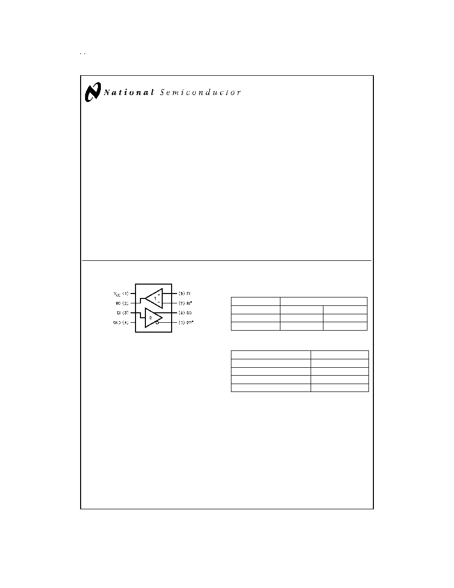
Connection Diagram
Truth Tables
Driver
Input
Outputs
DI
DO
DO
*
H
H
L
L
L
H
Receiver
Inputs
Output
RIRI
*
RO
V
DIFF
+200 mV
H
V
DIFF
-200 mV
L
OPEN
H
Non-terminated
DS011753-1
Order Number DS89C21TM
See NS Package Number M08A
June 1998
DS89C21
Differential
CMOS
Line
Driver
and
Receiver
Pair
© 1998 National Semiconductor Corporation
DS011753
www.national.com
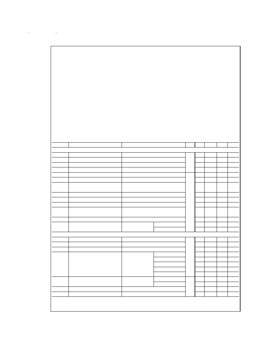
Absolute Maximum Ratings
(Note 1)
If Military/Aerospace specified devices are required,
please contact the National Semiconductor Sales Office/
Distributors for availability and specifications.
Supply Voltage (V
CC
)
7V
Driver Input Voltage (DI)
-1.5V to V
CC
+ 1.5V
Driver Output Voltage (DO,
DO
*
)
-0.5V to +7V
Receiver Input Voltage -- V
CM
(RI, RI
*
)
±
14V
Differential Receiver Input
±
14V
Voltage -- V
DIFF
(RI, RI
*
)
Receiver Output Voltage
(RO)
-0.5V to V
CC
+0.5V
Receiver Output Current
(RO)
±
25 mA
Storage Temperature Range
(T
STG
)
-65°C to +150°C
Lead Temperature (T
L
)
+260°C
(Soldering 4 sec.)
Maximum Junction
Temperature
150°C
Maximum Package Power Dissipation
@
+25°C
M Package
714 mW
Derate M Package
5.7 mW/°C above
+25°C
Recommended Operating
Conditions
Min
Max
Units
Supply Voltage (V
CC
)
4.50
5.50
V
Operating Temperature (T
A
)
-40
+85
°C
Input Rise or Fall Time (DI)
500
ns
Electrical Characteristics
(Notes 2, 3)
Over recommended supply voltage and operating temperature ranges, unless otherwise specified.
Symbol
Parameter
Conditions
Pin
Min
Typ
Max
Units
DRIVER CHARACTERISTICS
V
IH
Input Voltage HIGH
2.0
V
CC
V
V
IL
Input Voltage LOW
DI
GND
0.8
V
I
IH
, I
IL
Input Current
V
IN
= V
CC
, GND, 2.0V, 0.8V
0.05
±
10
µA
V
CL
Input Clamp Voltage
I
IN
= -18 mA
-1.5
V
V
OD1
Unloaded Output Voltage
No Load
DO,
DO
*
4.2
6.0
V
V
OD2
Differential Output Voltage
R
L
= 100
2.0
3.0
V
V
OD2
Change in Magnitude of V
OD2
5.0
400
mV
for Complementary Output States
V
OD3
Differential Output Voltage
R
L
= 150
2.1
3.1
V
V
OD4
Differential Output Voltage
R
L
= 3.9 k
4.0
6.0
V
V
OC
Common Mode Voltage
R
L
= 100
2.0
3.0
V
V
OC
Change in Magnitude of V
OC
2.0
400
mV
for Complementary Output States
I
OSD
Output Short Circuit Current
V
OUT
= 0V
-30
-115
-150
mA
I
OFF
Output Leakage Current
V
CC
= 0V
V
OUT
= +6V
0.03
+100
µA
V
OUT
= -0.25V
-0.08
-100
µA
RECEIVER CHARACTERISTICS
V
TL
, V
TH
Differential Thresholds
V
IN
= +7V, 0V, -7V
RI,
RI
*
-200
±
25
+200
mV
V
HYS
Hysteresis
V
CM
= 0V
20
50
mV
R
IN
Input Impedance
V
IN
= -7V, +7V, Other = 0V
5.0
9.5
k
I
IN
Input Current
Other Input = 0V,
V
IN
= +10V
+1.0
+1.5
mA
V
CC
= 5.5V and
V
IN
= +3.0V
0
+0.22
mA
V
CC
= 0V
V
IN
= +0.5V
-0.04
mA
V
IN
= -3V
0
-0.41
mA
V
IN
= -10V
-1.25
-2.5
mA
V
OH
Output HIGH Voltage
I
OH
= -6 mA
V
DIFF
= +1V
RO
3.8
4.9
V
V
DIFF
= OPEN
3.8
4.9
V
V
OL
Output LOW Voltage
I
OL
= +6 mA, V
DIFF
= -1V
0.08
0.3
V
I
OSR
Output Short Circuit Current
V
OUT
= 0V
-25
-85
-150
mA
www.national.com
2
Electrical Characteristics
(Notes 2, 3) (Continued)
Over recommended supply voltage and operating temperature ranges, unless otherwise specified.
Symbol
Parameter
Conditions
Pin
Min
Typ
Max
Units
DRIVER AND RECEIVER CHARACTERISTICS
I
CC
Supply Current
No Load
DI = V
CC
or GND
V
CC
3.0
6
mA
DI = 2.4V or 0.5V
3.8
12
mA
Switching Characteristics
(Note 3)
Over recommended supply voltage and operating temperature ranges, unless otherwise specified.
Symbol
Parameter
Conditions
Min
Typ
Max
Units
DIFFERENTIAL DRIVER CHARACTERISTICS
t
PLHD
Propagation Delay LOW to HIGH
R
L
= 100
(
Figures 2, 3)
2
4.9
10
ns
t
PHLD
Propagation Delay HIGH to LOW
C
L
= 50 pF
2
4.5
10
ns
t
SKD
Skew, |t
PLHD
t
PHLD
|
0.4
2.0
ns
t
TLH
Transition Time LOW to HIGH
(
Figures 2, 4)
2.2
9
ns
t
THL
Transition Time HIGH to LOW
2.1
9
ns
RECEIVER CHARACTERISTICS
t
PLH
Propagation Delay LOW to HIGH
C
L
= 50 pF
(
Figures 5, 6)
6
18
30
ns
t
PHL
Propagation Delay HIGH to LOW
V
DIFF
= 2.5V
6
17.5
30
ns
t
SK
Skew, |t
PLH
t
PHL
|
V
CM
= 0V
0.5
4.0
ns
t
r
Rise Time
(
Figure 7)
2.5
9
ns
t
f
Fall Time
2.1
9
ns
Note 1: "Absolute Maximum Ratings" are those values beyond which the safety of the device cannot be guaranteed. They are not meant to imply that the devices
should be operated at these limits. The tables of "Electrical Characteristics" specify conditions for device operation.
Note 2: Current into device pins is defined as positive. Current out of device pins is defined as negative. All voltages are referenced to ground unless otherwise
specified.
Note 3: All typicals are given for V
CC
= 5.0V and T
A
= 25°C.
Note 4: f = 1 MHz, t
r
and t
f
6 ns.
Note 5: ESD Rating: HBM (1.5 k
, 100 pF) all pins
2000V.
EIAJ (0
, 200 pF)
250V
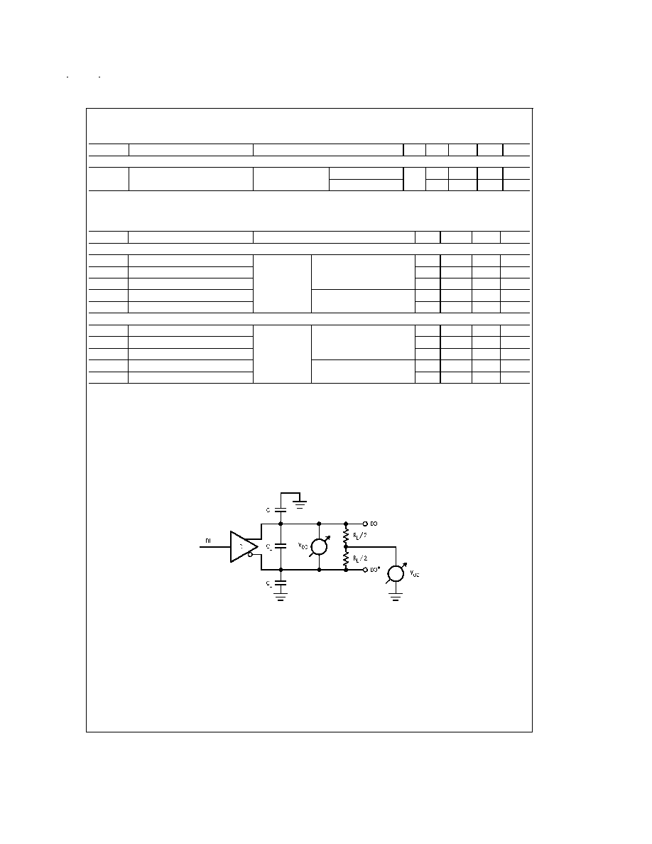
Parameter Measurement Information
DS011753-2
FIGURE 1. V
OD
and V
OC
Test Circuit
www.national.com
3
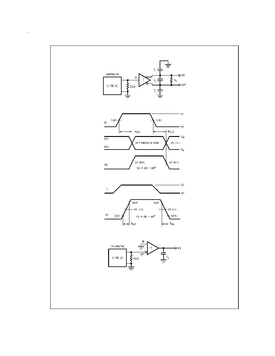
Parameter Measurement Information
(Continued)
DS011753-3
FIGURE 2. Driver Propagation Delay Test Circuit
DS011753-4
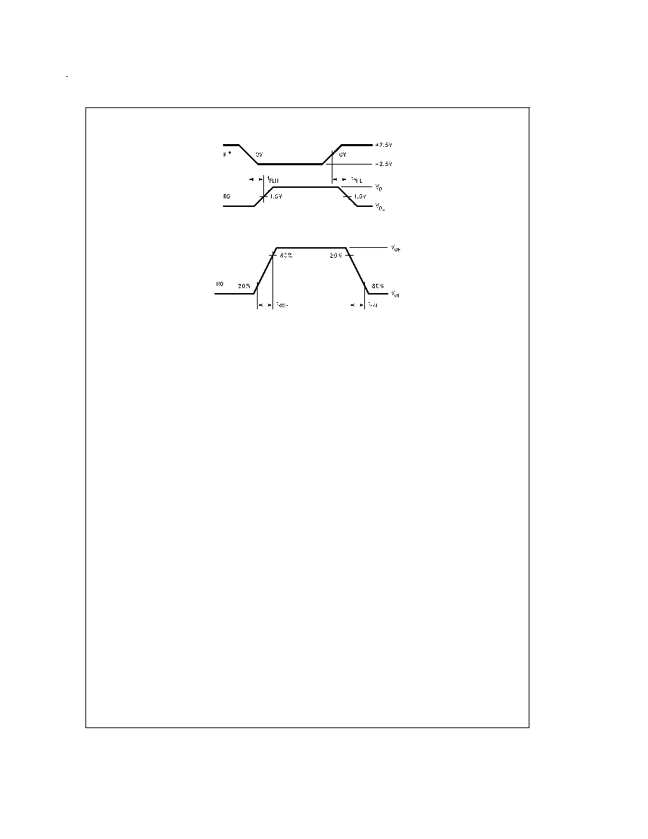
FIGURE 3. Driver Differential Propagation Delay Timing
DS011753-5
FIGURE 4. Driver Differential Transition Timing
DS011753-6
FIGURE 5. Receiver Propagation Delay Test Circuit
www.national.com
4
Parameter Measurement Information
(Continued)
DS011753-7
FIGURE 6. Receiver Propagation Delay Timing
DS011753-8
FIGURE 7. Receiver Rise and Fall Times
www.national.com
5