
General Description
The MAX3850 is a +3.3V DC-coupled laser driver for
SDH/SONET applications up to 2.7Gbps. The device
accepts differential data and clock inputs and provides
bias and modulation currents for driving a laser. If a
clock signal is available, a synchronizing input latch
can be used to reduce jitter. An automatic power-con-
trol (APC) feedback loop is incorporated to maintain a
constant average optical power over temperature and
lifetime. The wide modulation current range of 5mA to
60mA (up to 80mA AC-coupled) and bias current of
1mA to 100mA are easy to program, making this prod-
uct ideal for SDH/SONET applications. The MAX3850
also provides laser current-enable control, two current
monitors that are directly proportional to the laser bias
and modulation currents, and a failure-monitor output to
indicate when the APC loop is unable to maintain the
average optical power. Designed to be DC-coupled to
the laser with a supply voltage of only 3.3V, the
MAX3850 greatly simplifies interface requirements. The
MAX3850 is available in a small 32-pin QFN package
as well as dice.
Applications
Features
Single +3.3V Power Supply
35mA Supply Current
Programmable Bias Current from 1mA to 100mA
Programmable Modulation Current from 5mA to
60mA (Up to 80mA AC-Coupled)
Bias Current and Modulation Current Monitors
70ps Rise/Fall Time
Automatic Average Power Control with Failure
Monitor
Complies with ANSI, ITU, and Bellcore
SDH/SONET Specifications
Laser Current-Enable Control
MAX3850
2.7Gbps, +3.3V DC-Coupled
Laser Driver
________________________________________________________________
Maxim Integrated Products
1
SERIALIZER
WITH
CLOCK GEN
11
LD
16
50
8.0pF
3.3V
3.3V
0.01µF
BIASMON
MODMON
3.3V
1000pF
BIASMAX
LATCH
ENABLE
FAIL
MODSET
APCSET
APCFILT
GND
CLOCK-
CLOCK+
DATA-
DATA+
OUT+
BIAS
MD
OUT-
CAPC
MAX3850
MAX3890
100
100
TYPICAL APPLICATION CIRCUIT
WITH DC-COUPLED INPUTS
392
392
V
CC
0.1µF 0.1µF
Ordering Information
Typical Application Circuits
19-2294; Rev 1; 5/03
For pricing, delivery, and ordering information, please contact Maxim/Dallas Direct! at
1-888-629-4642, or visit Maxim's website at www.maxim-ic.com.
*Dice are designed to operate over this range, but are tested
and guaranteed at T
A
= +25°C only. Contact factory for
availability.
Covered by U.S. Patent numbers 5,802,089 and 5,883,910
Typical Application Circuits are continued at the end of the
data sheet.
Pin Configuration appears at the end of the data sheet.
PART
TEMP
RANGE
PIN-
PACKAGE
PACKAGE
CODE
MAX3850EGJ
- 40°C to + 85°C 32
QFN
G3255-1
MAX3850E/D
- 40°C to + 85°C Dice*
--
SDH/SONET Transmission
Systems
MPLS Transmitter Systems
Add/Drop Multiplexers
Digital Cross-Connects
Section Regenerators
EVALUATION KIT
AVAILABLE
MAX3850
2.7Gbps, +3.3V DC-Coupled Laser Driver
2
_______________________________________________________________________________________
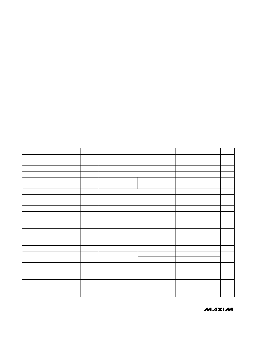
ABSOLUTE MAXIMUM RATINGS
DC ELECTRICAL CHARACTERISTICS
(V
CC
= +3.0V to +3.6V, T
A
= -40°C to +85°C. Typical values are at V
CC
= +3.3V, I
MOD
= 30mA, I
BIAS
= 60mA, T
A
= +25°C, unless
otherwise noted.) (Note 1)
Stresses beyond those listed under "Absolute Maximum Ratings" may cause permanent damage to the device. These are stress ratings only, and functional
operation of the device at these or any other conditions beyond those indicated in the operational sections of the specifications is not implied. Exposure to
absolute maximum rating conditions for extended periods may affect device reliability.
Supply Voltage, V
CC
..............................................-0.5V to +4.0V
Current into BIAS ............................................-20mA to +150mA
Current into OUT+, OUT- ................................-20mA to +100mA
Current into MD.....................................................-5mA to +5mA
Voltage at DATA+, DATA-, CLK+, CLK-, ENABLE, LATCH,
FAIL, BIASMON, MODMON, CAPC,
MODSET, BIASMAX, APCSET................-0.5V to (V
CC
+ 0.5V)
Voltage at APCFILT ...............................................-0.5V to +3.0V
Voltage at OUT+, OUT-.............................................0.4V to 4.8V
Voltage at BIAS............................................1.0V to (V
CC
+ 0.5V)
Continuous Power Dissipation (T
A
= +85°C)
32-Pin QFN (derate 21.2mW/°C above +85°C) ........13.84mW
Storage Temperature Range .............................-65°C to +165°C
Operating Junction Temperature Range ...........-55°C to +150°C
Processing Temperature (die) .........................................+400°C
Lead Temperature (soldering,10s) ..................................+300°C
PARAMETER
SYMBOL
CONDITIONS
MIN
TYP
MAX
UNITS
Supply Voltage
V
CC
3.0
3.3
3.6
V
Supply Current
I
CC
(Note 2)
35
65
mA
Bias-Current Range
I
BIAS
(Note 3)
1
100
mA
Bias Off-Current
I
BIAS-OFF
ENABLE = low (Note 4)
100
µA
I
BIAS
= 100mA
-480
12
480
Bias-Current Stability
APC open loop
I
BIAS
= 1mA
-1000
456
1000
ppm/°C
Differential Input Voltage Range
V
ID
(Figure 1)
200
1600
mV
P-P
Common-Mode Input Voltage
V
ICM
LVPECL compatible
V
CC
-
1.49
V
CC
-
1.32
V
CC
-
V
ID
/4
V
TTL Input High Voltage
ENABLE, LATCH
2.0
V
TTL Input Low Voltage
ENABLE, LATCH
0.8
V
TTL Output High Voltage
FAIL sourcing 50µA
2.4
V
CC
-
0.3
V
CC
V
TTL Output Low Voltage
Sinking 100µA
0
0.025
0.4
V
Monitor-Diode Reverse Bias
Voltage
1.5
V
Monitor-Diode DC Current Range
I
MD
18
1000
µA
I
MD
= 1mA
-480
95
480
Monitor-Diode Set-Point Stability
(Note 6)
I
MD
= 18µA
-1000
295
1000
ppm/°C
Monitor-Diode Bias Absolute
Accuracy
(Note 5)
-15
+15
%
BIASMON to I
BIAS
Gain
A
BIAS
I
BIAS
/I
BIASMON
36
41
46
A/A
MODMON to I
MOD
Gain
A
MOD
I
MOD
/I
MODMON
25
30
35
A/A
V
OUT
+, V
OUT
- = 0.6V (DC-coupled)
5
60
Modulation-Current Range
I
MOD
V
OUT
+, V
OUT
- = 2.0V (AC-coupled)
5
80
mA

MAX3850
2.7Gbps, +3.3V DC-Coupled Laser Driver
_______________________________________________________________________________________
3
DC ELECTRICAL CHARACTERISTICS (continued)
(V
CC
= +3.0V to +3.6V, T
A
= -40°C to +85°C. Typical values are at V
CC
= +3.3V, I
MOD
= 30mA, I
BIAS
= 60mA, T
A
= +25°C, unless
otherwise noted.) (Note 1)
AC ELECTRICAL CHARACTERISTICS
(V
CC
= +3.0V to +3.6V, I
MOD
= 5mA to 60mA, T
A
= -40°C to +85°C. Typical values are at V
CC
= +3.3V, I
MOD
= 30mA, T
A
= +25°C.)
(Note 7)
Note 1: Dice are tested at T
A
= +25°C only. Specifications at -40°C are guaranteed by design and characterization.
Note 2: Tested at R
MODSET
= 2.61k, R
BIASMAX
= 1.96k, excluding I
BIAS
and I
MOD
.
Note 3: Voltage on BIAS pin is (V
CC
- 1.5V).
Note 4: The bias and modulation currents will be switched off if any of the current set pins are grounded.
Note 5: Accuracy refers to part-to-part variation.
Note 6: Assuming the laser-to-monitor diode transfer function does not change with temperature. Guaranteed by design and
characterization.
Note 7: AC characteristics are guaranteed by design and characterization using the characterization circuit of Figure 2.
Note 8: Measured with repeating 0000 1111 pattern, LATCH = high.
PARAMETER
SYMBOL
CONDITIONS
MIN
TYP
MAX
UNITS
Modulation Off-Current
I
MOD-OFF
ENABLE = low (Note 4)
100
µA
I
MOD
= 60mA
-480
66
480
Modulation-Current Stability
I
MOD
= 5mA
-1000
110
1000
ppm/°C
PARAMETER
SYMBOL
CONDITIONS
MIN
TYP
MAX
UNITS
Maximum Data Rate
2.7
Gbps
Input Latch Setup Time
t
SU
LATCH = high (Figure 3)
90
ps
Input Latch Hold Time
t
H
LATCH = high (Figure 3)
60
ps
Output Rise Time
t
R
20% to 80% ed g e sp eed s ( N ote 8)
66
110
ps
Output Fall Time
t
F
20% to 80% ed g e sp eed s ( N ote 8)
70
100
ps
30mA
I
MOD
60 (Note 8)
±2
Output Overshoot
I
MOD
= 5mA (Note 8)
±12
%
I
MOD
Enable/Startup Delay
270
ns
I
BIAS
Typical Startup Delay
APC open loop, C
APC
and C
APCFILT
= 0
370
ns
Output Random Jitter
RJ
OUT
(Note 8)
0.66
1.4
ps
RMS
Output Deterministic Jitter
TJ
OUT
LATCH = high, 2
7
- 1 PRBS with 80 inserted 0s
and 80 inserted 1s
8.6
50
ps
P-P

MAX3850
2.7Gbps, +3.3V DC-Coupled Laser Driver
4
_______________________________________________________________________________________
DATA+
DATA-
(DATA+) - (DATA-)
I
OUT
+
100mV MIN
800mV MAX
200mV
P-P
MIN
1600mV
P-P
MAX
I
MOD
Figure 1. Required Input Signal and Output Polarity
CLK
DATA
t
CLK
t
SU
t
H
Figure 3. Setup/Hold Time Definition
30
30
OUT+
BIAS
OUT-
15
OSCILLOSCOPE
50
75
30
0.5pF
1.0pF
Z
0
= 30
Z
0
= 30
V
CC
V
CC
V
CC
MAX3850
I
OUT+
Figure 2. Output Termination for Characterization

MAX3850
2.7Gbps, +3.3V DC-Coupled Laser Driver
_______________________________________________________________________________________
5
OPTICAL EYE DIAGRAM
(2.7Gbps, 130mm FP LASER
1.87Gbps FILTER, 32-QFN)
MAX3850 toc01
MITSUBISHI ML725C8F LASER DIODE
BIAS CURRENT ENABLE
STARTUP DELAY vs. C
APC
MAX3850 toc02
CAPC (F)
STARTUP DELAY (ms)
0.1µ
0.01µ
1000p
1.0
10
100
0.1
100p
1.0µ
ELECTRICAL EYE DIAGRAM
(I
MOD
= 25mA, 2
13
- 1 + 80 CID, 32 QFN)
MAX3850 toc03
58ps/div
ELECTRICAL EYE DIAGRAM
(I
MOD
= 60mA, 2
13
- 1 + 80 CID, 32 QFN)
MAX3850 toc04
58ps/div
ELECTRICAL EYE DIAGRAM
AC-COUPLED
(I
MOD
= 80mA, 2
13
- 1 + 80 CID, 32 QFN)
MAX3850 toc05
58ps/div
RANDOM JITTER vs. I
MOD
MAX3850 toc06
I
MOD
(mA)
RANDOM JITTER (psms)
50
40
30
20
0.2
0.4
0.6
0.8
1.0
1.2
1.4
1.6
1.8
2.0
0
10
60
DETERMINISTIC JITTER vs. I
MOD
MAX3850 toc07
I
MOD
(mA)
TOTAL JITTER (ps
P-P
)
50
40
30
20
5
10
15
20
25
30
0
10
60
I
BIASMAX
vs. R
BIASMAX
MAX3850 toc08
R
BIASMAX
()
I
BIASMAX
(mA)
10k
150
140
130
120
110
100
90
80
70
60
50
40
30
20
10
0
1k
100k
I
MOD
vs. R
MODSET
MAX3850 toc09
R
MODSET
()
I
MOD
(mA)
10k
10
20
30
40
50
60
70
0
1k
100k
Typical Operating Characteristics
(DC-coupled output, T
A
= +25°C, unless otherwise noted.)