Äîêóìåíòàöèÿ è îïèñàíèÿ www.docs.chipfind.ru
General Description
The MAX3747/MAX3747A multirate limiting amplifiers
function as data quantizers for OC-3 through OC-48 syn-
chronous optical network (SONET), Fibre-Channel, and
Gigabit Ethernet optical receivers. They are pin-for-pin
compatible with the SY88993V from Micrel
Semiconductor, Inc. The amplifiers accept a wide range
of input voltages and provide constant-level, current-
mode logic (CML) output voltages with controlled edge
speeds. The MAX3747 output voltage level is 500mVp-p
and the MAX3747A output voltage is 800mVp-p.
The MAX3747/MAX3747A limiting amplifiers feature a
programmable loss-of-signal detect (LOS) and an
optional disable function (DISABLE). Output disable can
be used to implement squelch.
The MAX3747/MAX3747A are available in a 3mm, 10-pin
µMAX® package ideal for small form-factor receivers.
Applications
Gigabit Ethernet SFP/SFF Optical Transceiver
Modules
1G/2G Fibre-Channel SFP/SFF Optical
Transceiver Modules
Multirate OC-3 to OC-48 FEC SFP/SFF Optical
Transceiver Modules
10G LX4 Transceiver Modules
Features
Pin Compatible with Micrel SY88993V
155Mbps to 3.2Gbps Operation
>57dB of Gain for the MAX3747 and MAX3747A
<10
-12
BER with 2mV
P-P
Input Amplitude
18mA Supply Current
Chatter-Free LOS with Programmable Threshold
Output DISABLE Function
PECL-Compatible Inputs
MAX3747/MAX3747A
155Mbps to 3.2Gbps, Low-Power SFP
Limiting Amplifiers
________________________________________________________________ Maxim Integrated Products
1
Ordering Information
MAX3745
SUPPLY FILTER
V
CC
MAX4004
V
CC
DS1859
3-INPUT
DIAGNOSTIC
MONITOR
SFP OPTICAL RECEIVER
5-PIN TO-HEADER
HOST BOARD
HOST FILTER
SERDES
50
50
MAX3747
MAX3747A
V
REF
TH
GND LOS
DISABLE
IN-
IN+
OUT-
OUT+
V
CC
0.1
µF
0.1
µF
0.1
µF
0.1
µF
0.1
µF
0.1
µF
50
50
R1
R2
R1 + R2
5k
V
CC_
RX
V
CC_
HOST
LOS
4.7k
TO 10k
Typical Application Circuit
19-3297; Rev 0; 5/04
For pricing, delivery, and ordering information, please contact Maxim/Dallas Direct! at
1-888-629-4642, or visit Maxim's website at www.maxim-ic.com.
PART
TEMP RANGE
PIN-
PACKAGE
PKG
CODE
MAX3747EUB
-40°C to +85°C
10 µMAX
U10C-4
MAX3747AEUB
-40°C to +85°C
10 µMAX
U10C-4
Pin Configuration appears at end of data sheet.
µMAX is a registered trademark of Maxim Integrated Products, Inc.
MAX3747/MAX3747A
155Mbps to 3.2Gbps, Low-Power SFP
Limiting Amplifiers
2
_______________________________________________________________________________________
ABSOLUTE MAXIMUM RATINGS
ELECTRICAL CHARACTERISTICS
(V
CC
= +2.97V to +3.63V, CML output load is 50
to V
CC
, T
A
= -40°C to +85°C. Typical values are at V
CC
= +3.3V and T
A
= +25°C,
unless otherwise specified.) (Note 1)
Stresses beyond those listed under "Absolute Maximum Ratings" may cause permanent damage to the device. These are stress ratings only, and functional
operation of the device at these or any other conditions beyond those indicated in the operational sections of the specifications is not implied. Exposure to
absolute maximum rating conditions for extended periods may affect device reliability.
Power-Supply Voltage (V
CC
) .................................-0.5V to +4.5V
Voltage at IN+, IN- ..........................(V
CC
- 2.4V) to (V
CC
+ 0.5V)
Voltage at DISABLE, LOS, TH, V
REF
..........-0.5V to (V
CC
+ 0.5V)
Current into LOS ...................................................-1mA to +9mA
Current into V
REF
..................................................................2mA
Differential Input Voltage (IN+ - IN-) .....................................2.5V
Continuous Current at CML Outputs
(OUT+, OUT-) ..............................................-25mA to +25mA
Continuous Power Dissipation (T
A
= +70°C)
10-Pin µMAX (derate 6.9mW/°C above +70°C) ...........552mW
Operating Junction Temperature Range (TJ) .......-55°C to +150°C
Storage Ambient Temperature Range (TS)...........-55°C to +150°C
PARAMETER
SYMBOL
CONDITIONS
MIN
TYP
MAX
UNITS
POWER SUPPLY
MAX3747 includes the CML output current
30
35
MAX3747A includes the CML output current
36
41
Supply Current (Note 2)
I
CC
MAX3747/MAX3747A exclude the CML
output current
18
24
mA
Power-Supply Noise Rejection
PSNR
f < 2MHz
30
dB
INPUT SPECIFICATION
Input Sensitivity
V
IN-MIN
(Note 3)
4
mV
P-P
Input Overload
V
IN-MAX
(Note 3)
1200
mV
P-P
OUTPUT SPECIFICATION
Output Resistance
R
OUT
42
50
58
Differential Output Return Loss
DUT is powered on, f < 3GHz
15
dB
MAX3747A 4mV
P-P
V
IN
1200mV
P-P
600
800
1000
CML Differential Output Voltage
MAX3747 4mV
P-P
V
IN
1200mV
P-P
400
500
600
mV
P-P
Differential Output Signal When
Disabled
AC-coupled outputs, V
IN-MAX
applied to the
input (Note 4)
15
mV
P-P
Data-Output Transition Time
20% to 80% (Note 4)
70
120
ps
TRANSFER CHARACTERISTIC
K28.5 pattern at 3.2Gbps
13.2
19
PRBS 2
23
- 1 equivalent pattern at 2.7Gbps
(Note 6)
14
25
K28.5 pattern at 2.1Gbps
12
17
Deterministic Jitter (Notes 4, 5)
DJ
PRBS 2
23
- 1 equivalent pattern at 155Mbps
(Note 6)
85
150
ps
P-P
Random Jitter
V
IN
= 4mV
P-P
(Notes 4, 7)
3.5
5
ps
RMS
Input-Referred Noise
V
IN
= 4mV
P-P
(Note 4)
120
150
µV
RMS
Low-Frequency Cutoff
6.4
kHz
MAX3747/MAX3747A
155Mbps to 3.2Gbps, Low-Power SFP
Limiting Amplifiers
_______________________________________________________________________________________
3
ELECTRICAL CHARACTERISTICS (continued)
(V
CC
= +2.97V to +3.63V, CML output load is 50
to V
CC
, T
A
= -40°C to +85°C. Typical values are at V
CC
= +3.3V and T
A
= +25°C,
unless otherwise specified.) (Note 1)
PARAMETER
SYMBOL
CONDITIONS
MIN
TYP
MAX
UNITS
LOSS OF SIGNAL
LOS Hysteresis
10log(V
DEASSERT
/ V
ASSERT
) (Note 4)
1.25
dB
LOS-Assert/Deassert Time
(Notes 4, 8)
2.3
40.0
µs
Low LOS Assert Level
V
TH
= -1.3V (Notes 4, 9)
2.5
4.1
5.9
mV
P-P
Low LOS Deassert Level
V
TH
= -1.3V (Notes 4, 9)
6.2
9.3
mV
P-P
Medium LOS Assert Level
V
TH
= -0.68V (Notes 4, 9)
22
29
31
mV
P-P
Medium LOS Deassert Level
V
TH
= -0.68V (Notes 4, 9)
44.8
57
mV
P-P
High LOS Assert Level
V
TH
= -0.114V (Notes 4, 9)
36.0
53.7
63.6
mV
P-P
High LOS Deassert Level
V
TH
= -0.114V (Notes 4, 9)
86
115
mV
P-P
TTL/CMOS I/O
V
REF
Voltage
V
REF
V
CC
-
1.35
V
CC
-
1.3V
V
CC
-
1.19
V
LOS Output High Voltage
V
OH
R
LOS
= 4.7k
to 10k to V
CC_HOST
(3V)
2.4
V
LOS Output Low Voltage
V
OL
R
LOS
= 4.7k
to 10k to V
CC_HOST
(3.6V)
0.4
V
DISABLE Input High
V
IH
2.0
V
DISABLE Input Low
V
IL
0.8
V
DISABLE Input Current
R
LOS
= 4.7k
to 10k to V
CC_HOST
10
µA
Note 1: The data-input transition time is controlled by a 4th-order Bessel filter with f
-3dB
= 0.75 x 2.667GHz for all data rates of
2.667Gbps and below. The f
-3db
= 0.75 x 3.2GHz for a data rate of 3.2Gbps.
Note 2: Supply current is measured with unterminated outputs or with AC-coupled output termination (see Figure 1).
Note 3: Between sensitivity and overload, all AC specifications are met and the output is 0.95 x limited output amplitude.
Note 4: Guaranteed by design and characterization.
Note 5: The deterministic jitter (DJ) caused by the input filter is not included in the DJ generation specification.
Note 6: The PRBS 2
23
- 1 equivalent pattern consists of a K28.5 pattern plus 240 ones plus K28.5 pattern plus 240 zeros.
Note 7: Random jitter was measured without using a filter at the input.
Note 8: The signal at the input is switched between two amplitudes, Signal_ON and Signal_OFF, as shown in Figure 2.
Note 9: V
TH
is the voltage at pin 5 referenced to V
CC
(see Figure 5).
MAX3747/MAX3747A
155Mbps to 3.2Gbps, Low-Power SFP
Limiting Amplifiers
4
_______________________________________________________________________________________
MAX3747
MAX3747A
V
CC
I
CC
(SUPPLY
CURRENT)
I
OUT
(CML OUTPUT
CURRENT)
50
50
Figure 1. Power-Supply Current Measurement
1dB
6dB
0V
V
IN
TIME
SIGNAL ON
MAXIMUM DEASSERT LEVEL
MINIMUM ASSERT LEVEL
SIGNAL OFF
MAXIMUM POWER-DETECT WINDOW
Figure 2. LOS Deassert Threshold--Set 1dB Below the
Minimum by Receiver Sensitivity
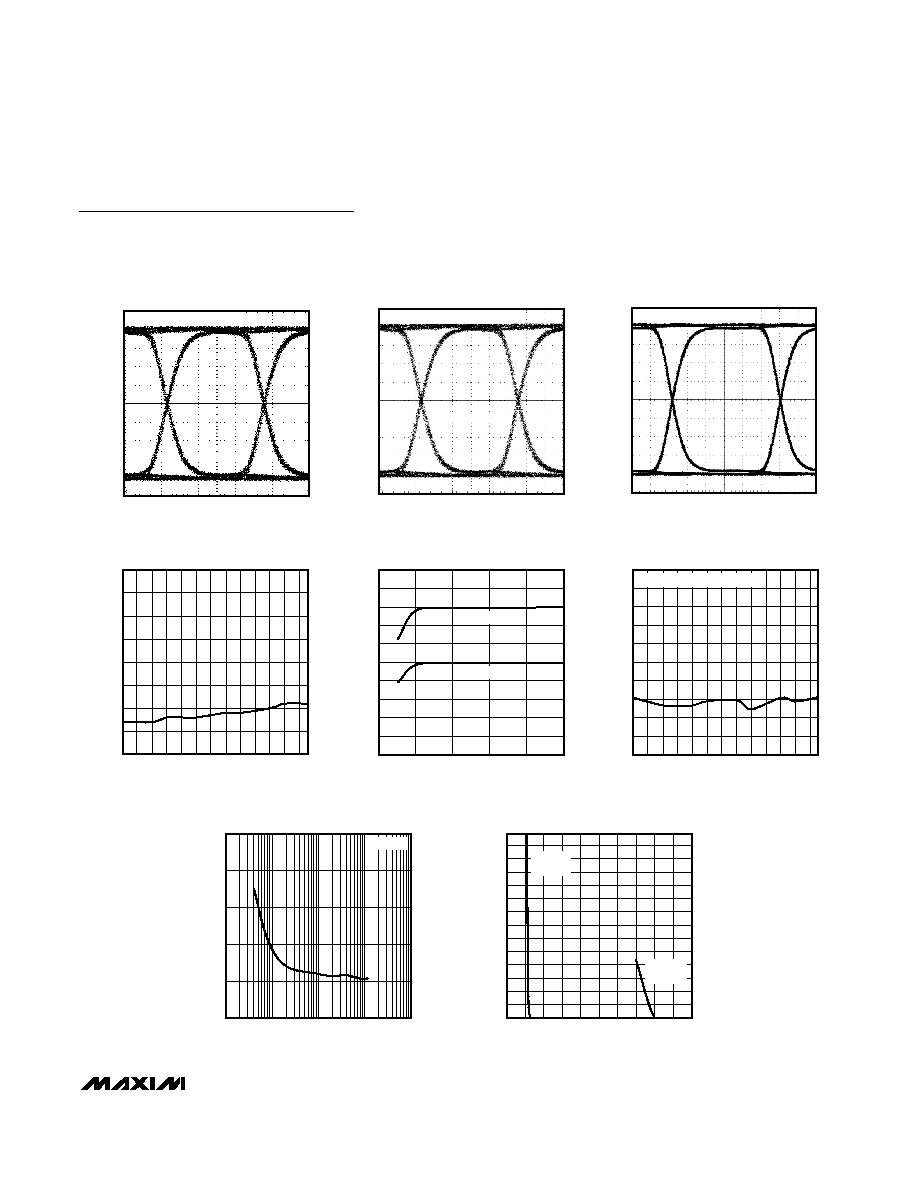
OUTPUT EYE DIAGRAM
(MINIMUM INPUT)
MAX3747/MAX3747A toc01
60mV/div
50ps/div
3.2Gbps, 2
23
- 1 PRBS, 4mV
P-P
OUTPUT EYE DIAGRAM
(MAXIMUM INPUT)
MAX3747/MAX3747A toc02
60mV/div
50ps/div
3.2Gbps, 2
23
- 1 PRBS, 1200mV
P-P
Typical Operating Characteristics
(V
CC
= +3.3V, T
A
= +25°C, unless otherwise noted.)
MAX3747/MAX3747A
155Mbps to 3.2Gbps, Low-Power SFP
Limiting Amplifiers
_______________________________________________________________________________________
5
OUTPUT EYE DIAGRAM
(MINIMUM INPUT)
MAX3747/MAX3747A toc03
60mV/div
70ps/div
2.7Gbps, 2
23
- 1 PRBS, 4mV
P-P
OUTPUT EYE DIAGRAM
(MAXIMUM INPUT)
MAX3747/MAX3747A toc04
60mV/div
70ps/div
2.7Gbps, 2
23
- 1 PRBS, 1200mV
P-P
OUTPUT EYE DIAGRAM AT +100
°C
MAX3747/MAX3747A toc05
60mV/div
80ps/div
2.125Gbps, CJTPAT, 50mV
P-P
10
25
20
15
30
35
45
40
50
-40
-20 -10
-30
0 10 20 30 40 50 60 70 80
SUPPLY CURRENT vs. TEMPERATURE
(EXCLUDES OUTPUT CURRENT)
MAX3747/MAX3747A toc06
TEMPERATURE (°C)
SUPPLY CURRENT (mA)
TRANSFER FUNCTION
(OUTPUT VOLTAGE vs. INPUT VOLTAGE)
MAX3747/MAX3747A toc07
DIFFERENTIAL INPUT (mV
P-P
)
DIFFERENTIAL OUTPUT (mV
P-P
)
4
3
2
1
100
200
300
400
500
600
700
800
900
1000
0
0
5
MAX3747A
MAX3747
0
1.5
1.2
0.9
0.6
0.3
1.8
2.1
2.7
2.4
3.0
-40
-20 -10
-30
0 10 20 30 40 50 60 70 80
RANDOM JITTER vs. TEMPERATURE
MAX3747/MAX3747A toc08
TEMPERATURE (°C)
RANDOM JITTER (ps
RMS
)
V
IN
= 50mV
P-P
, FREQ = 2.7Gbps
RANDOM JITTER vs. INPUT AMPLITUDE
MAX3747/MAX3747A toc09
DIFFERENTIAL INPUT AMPLITUDE (mV
P-P
)
RANDOM JITTER (ps
RMS
)
1000
100
10
1
2
3
4
5
0
1
10,000
3.2Gbps
BIT-ERROR RATIO vs. INPUT VOLTAGE
MAX3747/MAX3747A toc10
DIFFERENTIAL INPUT AMPLITUDE (mV
P-P
)
BIT-ERROR RATIO (10
-12
)
9
8
6
7
2
3
4
5
1
1000
2000
3000
4000
5000
6000
7000
8000
9000
10,000
11,000
12,000
13,000
1
0
10
MAXIM
MAX3747
MICREL
SY88993V
Typical Operating Characteristics (continued)
(V
CC
= +3.3V, T
A
= +25°C, unless otherwise noted.)