MAX3524 Full Data Sheet (PDF)
General Description
The MAX3524 broadband amplifier is designed specifi-
cally for cable television receiver and cable modem
applications. The MAX3524 is a single-ended input, dif-
ferential-output low-noise amplifier (LNA) that offers
15dB of gain. It operates from a +4.75V to +5.25V sin-
gle supply from 44MHz to 880MHz. The MAX3524
includes an operational amplifier that is used to control
an off-chip PIN attenuator circuit at the input of the
LNA. The attenuator is typically used to regulate the
input signal to a value that maintains high linearity for
large signals. The MAX3524 is available in a 10-pin
µMAX package with an exposed paddle (EP) and oper-
ates in the extended temperature range (-40°C to
+85°C).
Applications
Cable Modem
Cable Set-Top Box
Broadband Amplifier
CATV Infrastructure
Features
o Single-Ended Input, Differential Output
o +4.75V to +5.25V Single-Supply Operation
o Broadband Operation: 44MHz to 880MHz
o Low Noise Figure: 4.2dB
o High Linearity: IIP2 (42dBm), IIP3(14dBm)
o Voltage Gain: 15dB
o Independent On-Chip Op Amp
MAX3524
Low-Noise, High-Linearity
Broadband Amplifier
________________________________________________________________ Maxim Integrated Products
1
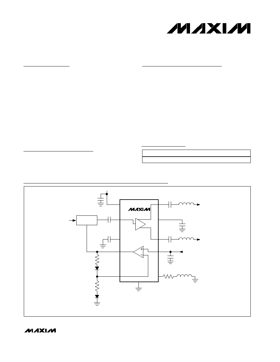
OPIN-
R2
3k
10nF
D2
CMDSH-3
D1
CMDSH-3
R1
3k
FROM DEMOD IC
TO CONTROL PIN
ATTENUATOR
L1 = 0.5 TO 1nH
L2 = 0.5 TO 1nH
C
L
< 1.8pF
OUTPUT TO TUNER
(DIFFERENTIAL DRIVE)
RFOUT+
RFIN
1
2
RFGND
GND
*EXPOSED PADDLE
INPUT:
44-880MHz
75-2k
OPOUT
PIN
ATTENUATOR
OPIN+
RFOUT-
V
CC
R
BIAS
= 5.9
L
BIAS
= 680nH
0.1
µF
0.1
µF
10
µF
0.1
µF
0.1
µF
V
CC
= 5V
10
µF
V
CC
= 5V
V
CC
OP AMP
BIAS
MAX3524
*
3
4
5
10
9
8
7
6
Typical Application Circuit
19-1764; Rev 0; 7/00
For price, delivery, and to place orders, please contact Maxim Distribution at 1-888-629-4642,
or visit Maxim's website at www.maxim-ic.com.
Pin Configuration appears at end of data sheet.
Ordering Information
PART
TEMP. RANGE
PIN-PACKAGE
MAX3524EVB
-40
°C to +85°C
10
µMAX-EP*
*Exposed paddle
MAX3524
Low-Noise, High-Linearity
Broadband Amplifier
2
_______________________________________________________________________________________
ABSOLUTE MAXIMUM RATINGS
DC ELECTRICAL CHARACTERISTICS
(Typical Application Circuit, V
CC
= +4.75V to +5.25V, R
BIAS
= 5.9
, L
BIAS
= 680nH, T
A
= -40°C to +85°C, unless otherwise indicat-
ed. Typical values measured at V
CC
= +5.0V, T
A
= +25°C.) (Notes 1, 2)
AC ELECTRICAL CHARACTERISTICS
(MAX3524 EV kit as shown in Figure 1, V
CC
= +4.75V to +5.25V, P
RFIN
= -20dBm, Z
S
= 75
, R
BIAS
= 5.9
, L
BIAS
= 680nH,
f
IN
= 44MHz, Z
L
= 50
|| 2pF, T
A
= +25°C. Typical values are at V
CC
= +5V, unless otherwise indicated.) (Notes 2, 3)
Stresses beyond those listed under "Absolute Maximum Ratings" may cause permanent damage to the device. These are stress ratings only, and functional
operation of the device at these or any other conditions beyond those indicated in the operational sections of the specifications is not implied. Exposure to
absolute maximum rating conditions for extended periods may affect device reliability.
Note 1: Parameters are production tested at T
A
= +25°C and T
A
= +85°C. Limits are guaranteed by design and characterization for
T
A
= -40°C to +25°C.
Note 2: For optimum linearity, the DC resistance of L
BIAS
in series with R
BIAS
must be approximately 7.3
.
Note 3: Guaranteed by design and characterization.
Note 4: Gain is guaranteed over the operating frequency range, by design and characterization. Insertion loss of balun is subtracted.
Production tested at 44MHz and 880MHz.
Note 5: Corresponding voltage gain at R
L
= 3k
, calculated as in Figure 2.
Note 6: Frequencies and input power levels: 275MHz, 325MHz, and -20dBm per tone.
V
CC
to GND ...........................................................-0.3V to +7.0V
RFIN ....................................................................................+2.0V
P
RFIN
...................................................................................0dBm
R
BIAS (MINIMUM)
.......................................................................5
RFOUT+, RFOUT-, OPIN-, OPIN+, OPOUT...-0.3V to (V
CC
+ 0.3V)
RFOUT+, RFOUT- Short-Circuit Duration ...............................10s
Continuous Power Dissipation (T
A
= +70°C)
10-Pin µMAX (derate 10.3mW/°C above +70°C) .........825mW
Operating Temperature Range ...........................-40°C to +85°C
Storage Temperature Range .............................-65°C to +150°C
Junction Temperature ......................................................+150°C
Lead Temperature (soldering, 10s) .................................+300°C
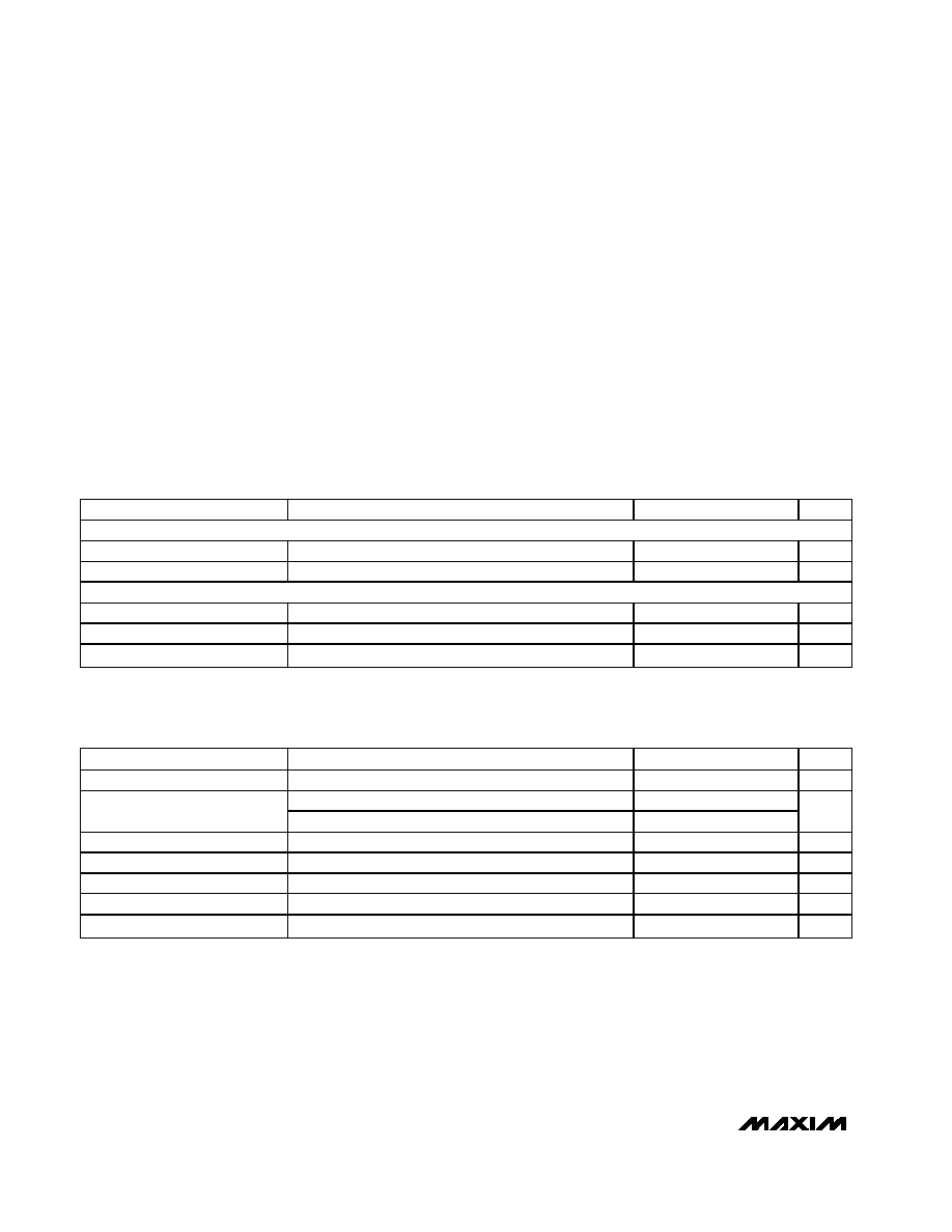
PARAMETERS
CONDITIONS
MIN
TYP
MAX
UNITS
SUPPLY
Supply Voltage
4.75
5.25
V
Supply Current
85
95
mA
OPERATIONAL AMPLIFIER
Common-Mode Input Range
0.5
3.0
V
Maximum Output Voltage
I
O
= 20mA
V
CC
- 0.5
V
Minimum Output Voltage
I
O
= 20mA
0.5
V
PARAMETERS
CONDITIONS
MIN
TYP
MAX
UNITS
Operating Frequency Range
44
880
MHz
T
A
= +25
°C
8.0
9.8
11
Power Gain (Note 4)
T
A
= -40
°C to +85°C
7.6
11.5
dB
Voltage Gain (Note 5)
R
L
= 3k
15
dB
Noise Figure (Note 3)
f
RFIN
= 300MHz
4.2
4.9
dB
IIP3 (Notes 3, 6)
12
14
dBm
IIP2 (Notes 3, 6)
40
42
dBm
Output-to-Input Isolation
f
RFIN
= 300MHz
40
60
dB
MAX3524
Low-Noise, High-Linearity
Broadband Amplifier
_______________________________________________________________________________________
3
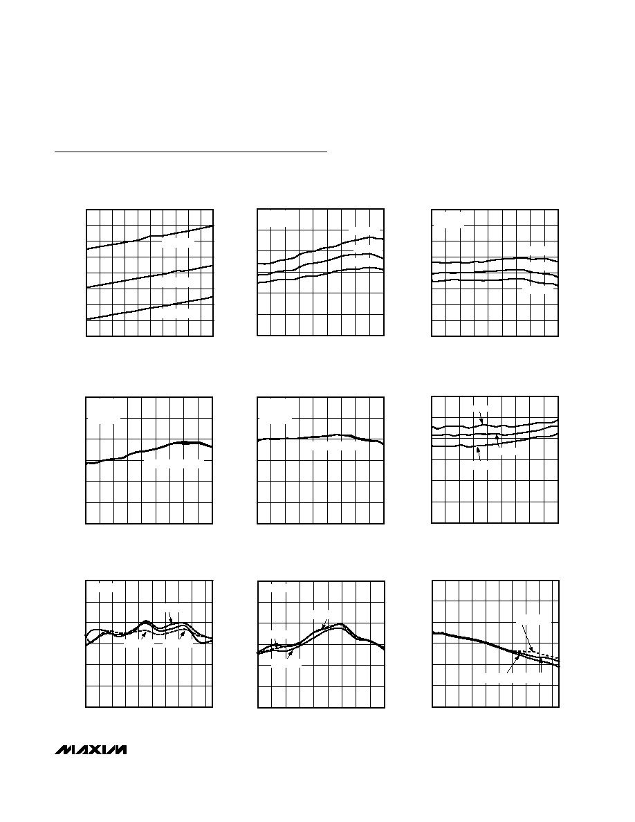
82
84
83
85
88
89
87
86
90
4.5
4.7 4.8 4.9 5.0
4.6
5.1 5.2 5.3 5.4 5.5
CURRENT vs. VOLTAGE
MAX3524toc01
V
CC
(V)
I
CC
(mA)
T
A
= +25
°C
T
A
= +85
°C
T
A
= -40
°C
6
7
8
9
10
11
12
40
240
140
340 440 540 640 740 840 940
POWER GAIN vs. FREQUENCY
MAX3524 toc02
FREQUENCY (MHz)
GAIN (dB)
T
A
= -45
°C
T
A
= +25
°C
T
A
= +85
°C
Zs = 50
C
L
= 1.5pF
6
8
7
11
10
9
13
12
14
40
340 440
140 240
540 640 740 840 940
POWER GAIN vs. FREQUENCY
MAX3524 toc03
FREQUENCY (MHz)
GAIN (dB)
T
A
= -40
°C
T
A
= +25
°C
T
A
= +85
°C
Zs = 75
C
L
= 1.5pF
6
7
8
9
10
11
12
40
240
140
340 440 540 640 740 840 940
POWER GAIN vs. FREQUENCY
MAX3524 toc04
FREQUENCY (MHz)
GAIN (dB)
T
A
= +25
°C
Z
s
= 50
C
L
= 1.5pF
V
CC
= 4.75, 5.00, 5.25
6
7
8
9
10
11
12
40
240
140
340 440 540 640 740 840 940
POWER GAIN vs. FREQUENCY
MAX3524 toc05
FREQUENCY (MHz)
GAIN (dB)
T
A
= +25
°C
Z
s
= 75
C
L
= 1.5pF
V
CC
= 4.75, 5.00, 5.25
0
1
2
3
4
5
6
40
240
140
340 440 540 640 740 840 940
NOISE FIGURE vs. FREQUENCY
MAX3524 toc06
FREQUENCY (MHz)
NOISE FIGURE (dB)
T
A
= +85
°C
T
A
= +25
°C
T
A
= -40
°C
8
14
12
10
16
18
20
50
450
350
150 250
550 650 750 850 950
IIP3 vs. FREQUENCY
MAX3524 toc07
FREQUENCY (MHz)
IIP3 (dBm)
T
A
= -40
°C
T
A
= +25
°C
T
A
= +85
°C
Zs = 75
30
35
40
45
50
55
60
100
300
200
400 500 600 700 800 900 1000
IIP2 vs. FREQUENCY
MAX3524 toc08
FREQUENCY (MHz)
IIP2 (dBm)
T
A
= -40
°C
T
A
= +25
°C
T
A
= +85
°C
Zs = 75
4
10
8
6
12
14
16
40
440
340
140 240
540 640 740 840 940
1dB COMPRESSED OUTPUT POWER
vs. FREQUENCY
MAX3524toc09
FREQUENCY (MHz)
P
OUT
(dBm)
V
CC
= 5.25V
V
CC
= 5.00V
V
CC
= 4.75V
Typical Operating Characteristics
(MAX3524 EV kit as shown in Figure 1, V
CC
= +5V, P
RFIN
= -20dBm, Z
L
= 50
|| 2pF, R
BIAS
= 5.9
, L
BIAS
= 680nH, insertion loss of
balun subtracted, T
A
= +25°C.)
MAX3524
Low-Noise, High-Linearity
Broadband Amplifier
4
_______________________________________________________________________________________
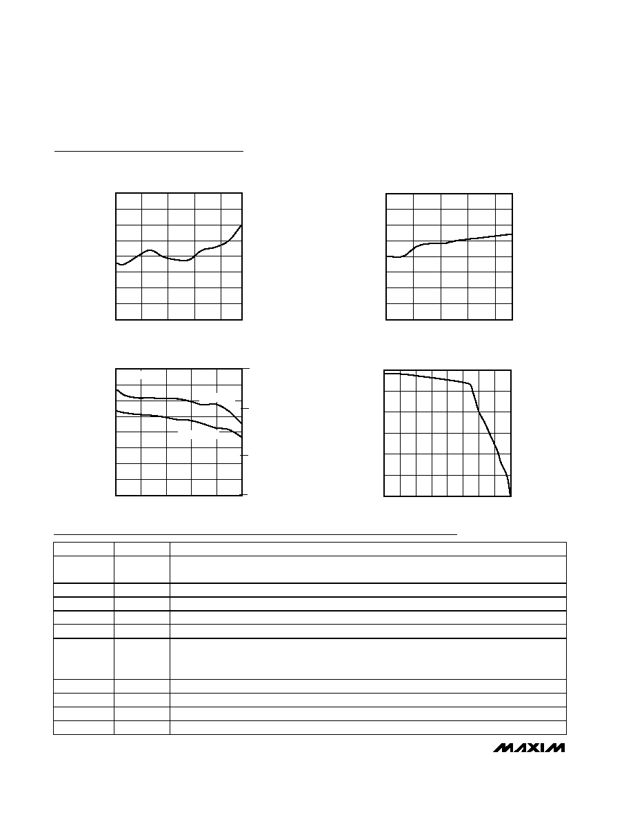
-80
-75
-70
-65
-60
-55
-50
-45
-40
20
70
120
170
220
PSRR vs. FREQUENCY
MAX3524toc11
FREQUENCY (MHz)
PSRR (dB)
Typical Operating Characteristics (continued)
(MAX3524 EV kit as shown in Figure 1, V
CC
= +5V, P
RFIN
= -20dBm, Z
L
= 50
|| 2pF, R
BIAS
= 5.9
, L
BIAS
= 680nH, insertion loss of
balun subtracted, T
A
= +25°C.)
0
50
100
150
200
250
300
350
400
40
240
440
640
840
RESISTANCE AND CAPACITANCE
vs. FREQUENCY
MAX3524 toc12
FREQUENCY (MHz)
RESISTANCE (
)
RESISTANCE
Z
IN
= R II C
CAPACITANCE
1
1.5
2.0
2.5
CAPACITANCE (pF)
Pin Description
PIN
NAME
FUNCTION
1, 9
V
CC
Supply Voltage Input. Connect both pins together. Bypass with a 10
µF and 47pF capacitor to
GND.
2
RFIN
RF Input of LNA. Requires DC blocking capacitor.
3
RFGND
Bypass to GND through 10nF capacitor.
4
OPOUT
Operational Amplifier Output
5
OPIN-
Inverting Input of Operational Amplifier
6
BIAS
LNA Bias Setting Pin. For nominal bias, connect 5.9
resistor in series with 680nH to GND
(total DC resistance = resistance of R
BIAS
+ DC resistance of the inductor = 7.3
). The value of
the resistor is adjusted to alter the current and therefore linearity of the LNA.
7
OPIN+
Noninverting Input of Operational Amplifier
8
RFOUT-
Inverting Output of LNA
10
RFOUT+
Noninverting Output of LNA
Slug
GND
Ground
0
1
2
3
4
5
6
0
1.0
0.5
1.5
2.0
2.5
3.0
3.5
4.0
OP AMP CLOSED-LOOP VOLTAGE GAIN
OF 2 vs. FREQUENCY
MAX3524 toc13
FREQUENCY (MHz)
V
GAIN
(dB)
-80
-75
-70
-65
-60
-55
-50
-45
-40
40
240
440
640
840
ISOLATION vs. FREQUENCY
MAX3524toc10
FREQUENCY (MHz)
ISOLATION (dB)
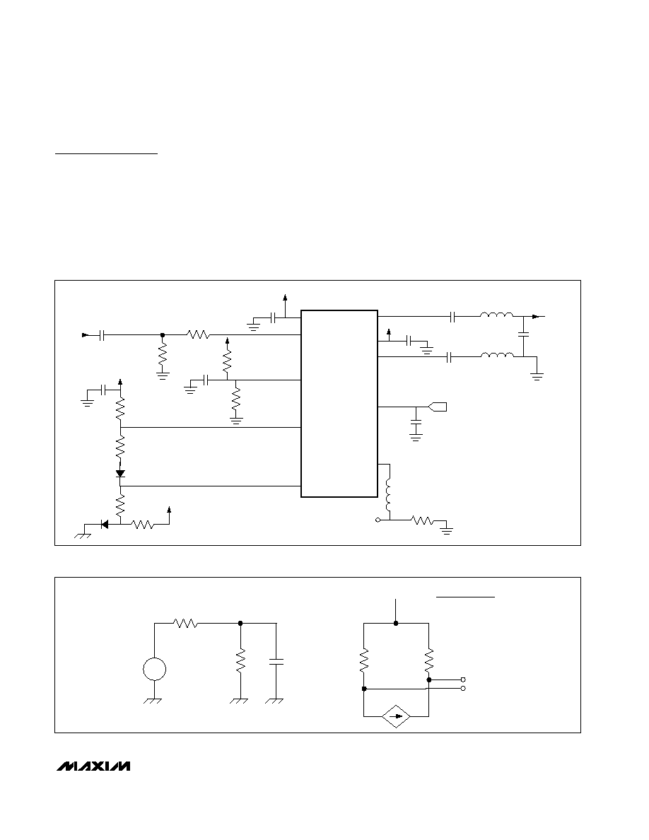
Detailed Description
The MAX3524 is a broadband amplifier with a single-
ended input and differential outputs, including an oper-
ational amplifier that can be used to control an external
attenuator circuit. Figure 1 is the MAX3524 EV kit
schematic.
Low-Noise Amplifier
The low-noise amplifier operates from 44MHz to
880MHz and is designed specifically for cable TV and
cable modem applications. The LNA provides 15dB of
insertion voltage gain (see Figure 2) when driving a
3k
load. At 300MHz, the noise figure is 4.2dB, IIP2
and IIP3 are 42dBm and 14dBm, respectively.
Operational Amplifier
The operational amplifier is suitable for interfacing to a
PIN attenuator circuit which is typically employed at the
input of the LNA. The common-mode input range is
0.5V to 3V and the output voltage swing is 0.5V to V
CC
-
0.5V while sinking or sourcing 20mA. Input bias current
and input offset voltage are 1µA and 1mV, respectively.
The open-loop voltage gain is greater than 10,000. The
MAX3524
Low-Noise, High-Linearity
Broadband Amplifier
_______________________________________________________________________________________
5
2V
IN
330
30
30
75
Z
S
RFIN
V
CC
(PIN9)
V1
0.06V1
1.8pF
RFOUT-
RFOUT+
A
V
= (V
RFOUT +
) - (V
RFOUT
-) = 5.7
V
IN
A
V
(dB) = 20log
10
A
V
= 15dB
Figure 2. LNA Equivalent Circuit and Open-Circuit Voltage Gain Calculation
RF INPUT
TO
ATTENUATOR
C11
0.1
µF
C10
0.1
µF
R9
100
R10
3k
D1
D2
R7
10k
VCC
C12
0.1
µF
R2
R4
50k
R3
50k
R1
13.3
VCC
C1
47pF
VCC
VCC
RFIN
RFGND
OP OUT
OP IN
R
BIAS
5.81
L
BIAS
0.1
µF
C2
2pF
C15
0.1
µF
C15
0.1
µF
C14
47pF
VCC
RF OUTPUT
RF OUT-
VCC2
RF OUT+
OPIN+
BIAS
R8
3k
D1, D2 SMALL-SIGNAL SCHOTTKY DIODES, TYPICALLY CMDSH-3
Figure 1. MAX3524 EV Kit Schematic