29701.indd
LTC2970/LTC2970-1
1
29701f
Dual I
2
C Power
Supply Monitor and
Margining Controller
The LTC
®
2970 is a dual power supply monitor and
margining controller with an SMBus compatible I
2
C bus
interface. A low-drift, on-chip reference and 14-bit
A/D
converter allow precise measurements of supply voltages,
load currents or internal die temperature. Fault manage-
ment allows
A
L
E
R
T to be asserted for confi gurable over
and under voltage fault conditions. Two voltage buffered,
8-bit IDACs allow highly accurate programming of DC/DC
converter output voltages. The IDACs can be confi gured
to automatically servo the power supplies to the desired
voltages using the ADC. The LTC2970-1 adds a tracking
feature that can be used to turn multiple power supplies
on or off in a controlled manner.
The bus address is set to 1 of 9 possible combinations by
pin strapping the ASEL0 and ASEL1 pins. The LTC2970/
LTC2970-1 are packaged in the 24-lead, 4mm
× 5mm
QFN package.
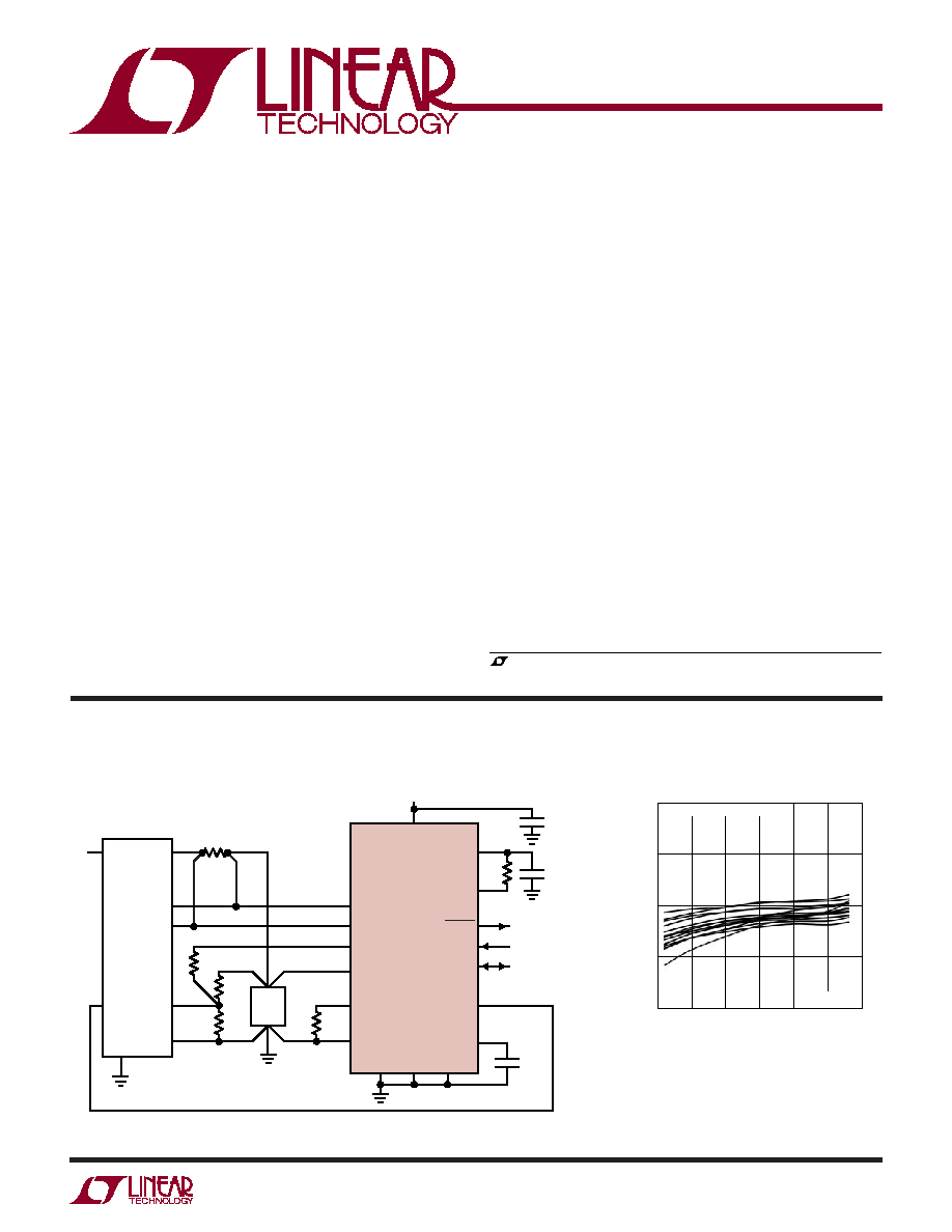
Dual Power Supply Voltage Servo
Monitoring Supply Voltage and Current
Programmable Power Supplies
Programmable Reference
Less Than ±0.5% Total Unadjusted Error 14-Bit
ADC with On-Chip Reference
Dual, 8-Bit IDACs with 1x Voltage Buffers
Linear, Voltage Servo Adjusts Supply Voltages by
Ramping IDAC Outputs Up/Down
I
2
CTM Bus Interface (SMBus Compatible)
Extensive, User Confi gurable Fault Monitoring
On-Chip Temperature Sensor
Available in 24-Lead 4mm
× 5mm QFN Package
Dual Power Supply Monitor and Controller (One of Two Channels Shown)
APPLICATIO S
U
FEATURES
DESCRIPTIO
U
TYPICAL APPLICATIO
U
, LTC and LT are registered trademarks of Linear Technology Corporation.
All other trademarks are the property of their respective owners.
8V TO 15V
OUT
FB
0.1
µF
0.1
µF
0.1
µF
I
I+
I
2
C BUS
SMBUS
COMPATIBLE
LOAD
DC/DC
CONVERTER
SGND
29701 TA01
RUN/SS
IN
V
IN
1/2 LTC2970
ALERT
SCL
SDA
GPIO_0
REF
12V
IN
GND
GND
ASEL0 ASEL1
V
DD
GPIO_CFG
V
IN0_BM
V
IN0_BP
V
IN0_AP
V
OUT0
I
OUT0
V
IN0_AM
(
)
TEMPERATURE (
°C)
50
ERROR (%)
0.25
0.25
25
75
29701 TA01b
0.50
25
0
50
0
0.50
100
ADC V
IN
= 5V
15 PARTS MOUNTED ON PCB
ADC Total Unadjusted Error
vs Temperature
LTC2970/LTC2970-1
2
29701f
Supply Voltages:
V
DD
......................................................... 0.3V to 6V
12V
IN
.................................................... 0.3V to 15V
Digital Input/Output Voltages:
ASEL0, ASEL1 ............................ 0.3V to V
DD
+ 0.3V
SDA, SCL, GPIO_CFG,
A
L
E
R
T, GPIO_0, GPIO_1 .......................... 0.3V to 6V
Analog Voltages:
V
IN0_AP
, V
IN0_AM
, V
IN0_BP
,
V
IN0_BM
, V
IN1_AP
, V
IN1_AM
,
V
IN1_BP
, V
IN1_BM
, V
OUT0
, V
OUT1
.............. 0.3V to 6V
I
OUT0
, I
OUT1
, REF ......................... 0.3V to V
DD
+ 0.3V
RGND .................................................... 0.3V to 0.3V
Operating Temperature Range:
LTC2970C ................................................ 0°C to 70°C
LTC2970I ............................................. 40°C to 85°C
Storage Temperature Range ................... 65°C to 125°C
Lead Temperature (Soldering, 10 sec) .................. 300°C
(Notes 1 and 2)
The
denotes the specifi cations which apply over the full operating
temperature range, otherwise specifi cations are at T
A
= 25°C. V
12VIN
= 12V, V
DD
and REF pins fl oating unless otherwise indicated,
C
VDD
= 100nF and C
REF
= 100nF.
ELECTRICAL CHARACTERISTICS
ABSOLUTE AXI U
RATI GS
W
W
W
U
SYMBOL
PARAMETER
CONDITIONS
MIN
TYP
MAX
UNITS
Power-Supply Characteristics
I
V12
12V
IN
Supply Current
V
12VIN
= 12V, V
DD
Floating
4.24
7.5
mA
I
DD
V
DD
Supply Current
V
DD
= 5V, V
12VIN
= V
DD
3.7
5
mA
V
LKO
V
DD
Undervoltage Lockout
V
DD
Ramping-Down, V
12VIN
= V
DD
3.7
4.14
4.4
V
V
DD
Undervoltage Lockout Hysteresis
118
mV
V
DD
Supply Input Operating Range
4.5
5.75
V
Regulator Output Voltage
8V V
12VIN
15V, 1mA I
VDD
0
4.75
4.95
5.25
V
Regulator Output Voltage
Temperature Coeffi cient
10
ppm/°C
Regulator Output Voltage Load
Regulation
1mA I
VDD
0
160
ppm/mA
Regulator Line Regulation
8V V
12VIN
15V, I
VDD
= 0mA
80
ppm/V
Regulator Output Short-Circuit Current V
12VIN
= 12V, V
DD
= 0V
5
34
63
mA
V
12VIN
12V
IN
Supply Operating Range
8
15
V
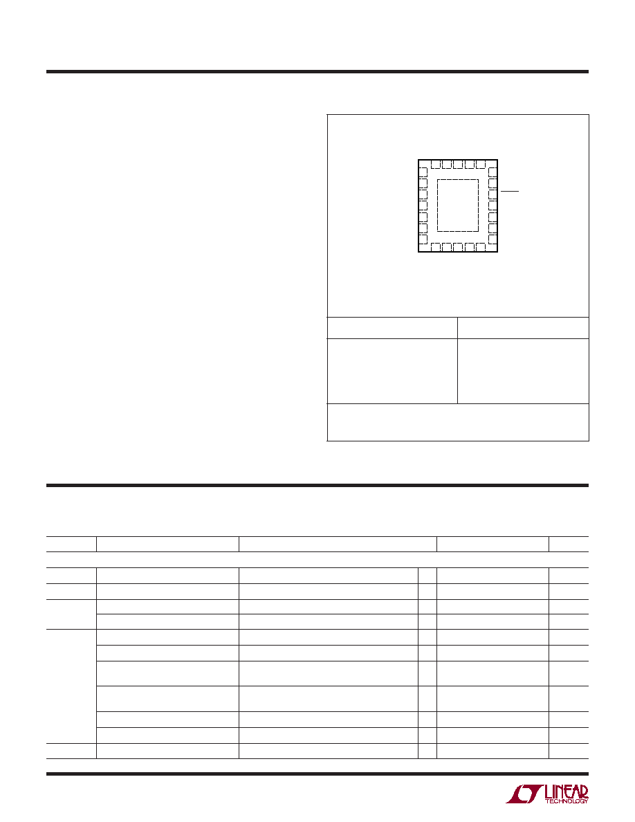
PACKAGE/ORDER I FOR ATIO
U
U
W
8
9
TOP VIEW
UFD PACKAGE
24-LEAD (4mm
× 5mm) PLASTIC QFN
10 11 12
24 23 22 21 20
25
6
5
4
3
2
1
V
IN0_AP
V
IN0_AM
V
IN0_BP
V
IN0_BM
V
IN1_AP
V
IN1_AM
V
IN1_BP
SDA
SCL
ALERT
GPIO_0
GPIO_1
I
OUT0
I
OUT1
RGND
REF
ASEL0
ASEL1
GPIO_CFG
V
IN1_BM
V
DD
12V
IN
V
OUT0
V
OUT1
7
14
15
16
17
18
19
13
T
JMAX
= 125°C,
JA
= 37°C/W
EXPOSED PAD (PIN 25) IS GND MUST BE SOLDERED TO PCB
ORDER PART NUMBER
UFD PART MARKING*
LTC2970CUFD
LTC2970IUFD
LTC2970CUFD-1
LTC2970IUFD-1
2970
2970
29701
29701
Order Options Tape and Reel: Add #TR
Lead Free: Add #PBF Lead Free Tape and Reel: Add #TRPBF
Lead Free Part Marking:
http://www.linear.com/leadfree/
Consult LTC Marketing for parts specifi ed with wider operating temperature
ranges. *The temperature grade is identifi ed by a label on the shipping
container.
LTC2970/LTC2970-1
3
29701f
The
denotes the specifi cations which apply over the full operating
temperature range, otherwise specifi cations are at T
A
= 25°C. V
12VIN
= 12V, V
DD
and REF pins fl oating unless otherwise indicated,
C
VDD
= 100nF and C
REF
= 100nF.
ELECTRICAL CHARACTERISTICS
SYMBOL
PARAMETER
CONDITIONS
MIN
TYP
MAX
UNITS
Voltage Reference Characteristics
V
REF
Reference Output Voltage
1.229
V
Reference Voltage Temperature
Coeffi cient
2
ppm/°C
Reference Overdrive Voltage Input
Range
1
1.5
V
ADC Characteristics
N_ADC
Resolution
N_ADC = 8.192V/16384
500
µV/LSB
TUE_ADC
Total Unadjusted Error
V
IN
= 3V, V
IN
= V
INn_xP
V
INn_xM
(Note 3)
±0.5
%
INL_ADC
Integral Nonlinearity
(Note 4)
1
2
4.5
LSB
DNL_ADC
Differential Nonlinearity
(Note 7)
±0.5
LSB
V
IN_ADC
Input Voltage Range
0
6
V
V
OS_ADC
Offset Error
1000
316
1000
µV
Offset Error Drift
0.19
µV/°C
GAIN_ADC
Gain Error
Full-Scale V
IN
= 6V
±0.4
%
Gain Error Drift
3
ppm/°C
T
CONV_ADC
Conversion Time
33.3
ms
C
IN_ADC
Input Sampling Capacitance
3
pF
F
IN_ADC
Input Sampling Frequency
61.4
kHz
I
LEAK_ADC
Input Leakage Current
0V < V
IN
< 6V
±0.1
µA
IDAC Output Current Characteristics
N_I
OUT
Resolution (Guaranteed Monotonic)
8
Bits
INL_I
OUT
Integral Nonlinearity
V
IOUTn
< V
DD
1.5V
±1
LSB
DNL_I
OUT
Differential Nonlinearity
V
IOUTn
< V
DD
1.5V
±1
LSB
I
FS-
I
OUT
Full-Scale Output Current
V
IOUTn
< V
DD
1.5V, DAC Code = 'hff
236
255
276
µA
I
DRIFT-
I
OUT
Output Current Drift
DAC Code = 'hff
32
ppm/°C
I
OS-
I
OUT
Offset Current
DAC Code = 'h00
±0.1
µA
Voltage Buffered IDAC Output Characteristics
INL_V
OUT
Integral Nonlinearity
R
IOUTn
= 10k
, No Load on V
OUTn
(Note 5)
±0.5
LSB
DNL_V
OUT
Differential Nonlinearity
R
IOUTn
= 10k
, No Load on V
OUTn
(Note 5)
±0.5
LSB
V
OS-
V
OUT
Offset Voltage
V
OS
= V
OUTn
V
IOUTn
, No Load on V
OUTn
1.6
±10
mV
Output Voltage Drift
No Load on V
OUTn
0.17
µV/°C
V
OUT
Load Regulation
0.1V < V
OUTn
< V
DD
1.5V, I
VOUTn
Source = 1mA
57
ppm/mA
0.1V < V
OUTn
< V
DD
1.5V, I
VOUTn
Sink = 1mA
100
ppm/mA
Leakage Current
V
OUTn
High-Z, 0V V
OUTn
V
DD
1
±100
nA
Short-Circuit Current Low
V
OUTn
Shorted to GND
50
mA
Short-Circuit Current High
V
OUTn
Shorted to V
DD
50
mA
LTC2970/LTC2970-1
4
29701f
The
denotes the specifi cations which apply over the full operating
temperature range, otherwise specifi cations are at T
A
= 25°C. V
12VIN
= 12V, V
DD
and REF pins fl oating unless otherwise indicated,
C
VDD
= 100nF and C
REF
= 100nF.
ELECTRICAL CHARACTERISTICS
SYMBOL
PARAMETER
CONDITIONS
MIN
TYP
MAX
UNITS
Soft Connect Comparator Characteristics (CMP0, CMP1)
V
OS
Offset Voltage
±3
mV
Temperature Sensor Characteristics
TMP
Gain
0.25
°C/LSB
12V
IN
Voltage Divider Characteristics
GAIN_12V
IN
Gain
0.329
0.333
0.335
V/V
Digital Inputs SCL, SDA, GPIO_CFG, GPIO_0, GPIO_1
V
IH
Input High Threshold Voltage
SDA, SCL
2.1
V
GPIO_CFG, GPIO_0, GIPO_1
1.6
V
V
IL
Input Low Threshold Voltage
SDA, SCL
1.5
V
GPIO_CFG, GPIO_0, GIPO_1
1.0
V
V
HYST
Input Hysteresis
0.08
V
I
LEAK
Input Leakage Current
0V V
IN
6V
±1
µA
C
IN
Input Capacitance
10
pF
Three State Inputs ASEL[1:0]
V
IH_ASEL
Input High Threshold Voltage
V
DD
0.5
V
V
IL_ASEL
Input Low Threshold Voltage
0.5
V
I
IN,HL
High, Low Input Current
ASEL[1:0] = 0, V
DD
±20
µA
I
IN,Z
High Z Input Current
±2
µA
Open Drain Outputs SDA, GPIO_CFG, GPIO_0, GPIO_1,
A
L
E
R
T
V
OL
Output Low Voltage
I
SINK
= 3mA
0.4
V
I
OH
Input Leakage Current
0V V
IN
6V
±1
µA
SYMBOL
PARAMETER
CONDITIONS
MIN
TYP
MAX
UNITS
I
2
C Interface Timing Characteristics
f
SCL
Serial Clock Frequency
(Note 6)
10
400
kHz
t
LOW
Serial Clock Low Period
(Note 6)
1.3
µs
t
HIGH
Serial Clock High Period
(Note 6)
0.6
µs
t
BUF
Bus Free Time Between Stop and Start
(Note 6)
1.3
µs
t
HD,STA
Start Condition Hold Time
(Note 6)
600
ns
t
SU,STA
Start Condition Setup Time
(Note 6)
600
ns
t
SU,STO
Stop Condition Setup Time
(Note 6)
600
ns
t
HD,DAT
Data Hold Time (LTC2970 Receiving Data)
Data Hold Time (LTC2970 Transmitting Data)
(Note 6)
0
300
900
ns
ns
t
SU,DAT
Data Setup Time (LTC2970 Receiving Data)
(Note 6)
100
ns
t
SP
Pulse Width of Spike Suppressed
(Note 6)
98
ns
The
denotes the specifi cations which apply over the full operating temperature range, otherwise specifi cations are at T
A
= 25°C.
LTC2970/LTC2970-1
5
29701f
of the transfer curve. The deviation is measured from the center of the
quantization band.
Note 5: Nonlinearity is defi ned from the fi rst code that is greater than or
equal to the maximum offset specifi cation to code 255 (full-scale).
Note 6: Maximum capacitive load, C
B
, for SCL and SDA is 400pF. Data and
clock risetime (t
r
) and falltime (t
f
) are: (20 + 0.1 · C
B
)(ns) < t
r
< 300ns and
(20 + 0.1 · C
B
)(ns) < t
f
< 300ns. C
B
= capacitance of one bus line in pF.
SCL and SDA external pull-up voltage, V
IO
, is 3V < V
IO
< 5.5V.
Note 7: This specifi cation is guaranteed by design.
The
denotes the specifi cations which apply over the full operating
temperature range, otherwise specifi cations are at T
A
= 25°C.
ELECTRICAL CHARACTERISTICS
SYMBOL
PARAMETER
CONDITIONS
MIN
TYP
MAX
UNITS
t
SETUP_GPIO
GPIO_0 and GPIO_1 Setup Time
GPIO_0 and GPIO_1 input setup time
prior to the 26th rising SCL of an IO()
I
2
C read. These inputs must be valid and
stable by this time to be returned in the
IO() read result. (Note 6)
2.5
µs
t
HOLD_GPIO
GPIO_0 and GPIO_1 Hold Time
GPIO_0 and GPIO_1 input hold time
after the 26th rising SCL of an IO() I
2
C
read. These inputs must be held until
this amount of time has elapsed to be
returned in the IO() read result. (Note 6)
2.5
µs
t
OUT_GPIO
GPIO_0 and GPIO_1 Output Time
GPIO_0 and GPIO_1 output delay after
the 35th rising SCL of an I
2
C write. These
outputs will become high impedance or
begin driving low by this time. (Note 6)
2.5
µs
Internal Timers
t
TIMEOUT_SMB
Stuck BUS Timer
The LTC2970 will release the I
2
C bus and
terminate the current command if the
command is not completed before this
amount of time has elapsed.
24
32
39
ms
t
SETUP_ADC
ADC Channel Setup Time
After selecting a new ADC channel, the
LTC2970 will wait this amount of time
to allow the analog input to settle before
beginning an ADC conversion.
304
µs
t
TIMEOUT_
SYNC
Tracking SYNC Failure Timer
LTC2970-1 Only: The LTC2970-1 will
abort a pending SYNC() command if a
tracking command is not received before
this amount of time has elapsed.
255
ms
t
HOLD_TRACK
Tracking IDAC Disconnect Delay
LTC2970-1 Only: After the tracking
algorithm asserts CPIO_CFG low, the
LTC2970-1 will delay disconnecting the
IDACs from the power supply feedback
nodes by this amount of time. Used while
tracking power supplies on.
32
ms
t
SETUP_TRACK
Tracking IDAC Disconnect Delay
LTC2970-1 Only: After the tracking
algorithm asserts CPIO_CFG high, the
LTC2970-1 will wait this amount of time
before starting to decrement Chn_a_
delay_track[9:0]. Used while tracking
power supplies off.
32
ms
t
DEC_TRACK
Tracking IDAC Decrement Rate
LTC2970-1 Only: The LTC2970-1 changes
Chn_a_delay_track[9:0] at this rate.
88
µs/LSB
Note 1: Stresses beyond those listed under Absolute Maximum Ratings
may cause permanent damage to the device. Exposure to any Absolute
Maximum Rating condition for extended periods may affect device
reliability and lifetime.
Note 2: All currents into device pins are positive; all currents out of device
pins are negative. All voltages are referenced to ground unless otherwise
specifi ed.
Note 3: TUE (%) is defi ned as % Gain Error + (INL · 500V/LSB + V
OS
) · 100
Note 4: Integral nonlinearity (INL) is defi ned as the deviation of a code
from a straight line passing through the actual endpoints (0V and 6V)
V
IN