2920-1/2 Layout
LTC2920-1/LTC2920-2
1
292012i
Single/Dual Power Supply
Margining Controller
March 2003
Information furnished by Linear Technology Corporation is believed to be accurate and reliable.
However, no responsibility is assumed for its use. Linear Technology Corporation makes no represen-
tation that the interconnection of its circuits as described herein will not infringe on existing patent rights.
The LTC
®
2920 allows power supplies and power supply
module output voltages to be precisely adjusted both up
and down for automated PCB testing. The power supply
output voltage is changed by sourcing or sinking current
into the feedback node or voltage adjust pin of the power
supply. This allows a system to test the correct operation
of electrical components at the upper and/or lower power
supply voltage limits specified for a given design (Power
Supply "Margining").
The LTC2920 uses a single resistor to set the voltage
margining current. The margining current is adjustable
over a 400:1 range. Precision margin currents can be
supplied to within 0.6V of ground or V
CC
.
The LTC2920-1 is a single margining controller. The
LTC2920-2 has two independently controllable margining
channels. Each channel has its own control pin and current
setting resistor. The LTC2920-2 can be used to symmetri-
cally margin two power supplies, or asymmetrically mar-
gin a single power supply.
Both the LTC2920-1 and LTC2920-2 feature a trimmed on-
board voltage reference. Typical power supply margining
accuracy is better than 0.4%.
s
Automated PCB Production Testing
s
Automated Preventative Maintenance Testing
s
DC/DC Converter Module Margining
, LTC and LT are registered trademarks of Linear Technology Corporation.
APPLICATIO S
U
FEATURES
DESCRIPTIO
U
TYPICAL APPLICATIO
U
Final Electrical Specifications
s
Margin Voltage Precision <0.4%
s
400:1 Current Programming Range
s
Symmetric/Asymmetric High and Low Voltage
Margining
s
Single Control Pin per Supply--High, Float, Low
s
Single Current Setting Resistor per Supply
s
Wide V
CC
Compliance 2.2V < V
CC
< 6V
s
Wide Output Compliance
0.6V < V
MARGIN
< (V
CC
0.6V)
s
Single in 5-Pin ThinSOT
TM
(LTC2920-1)
s
Dual in 8-Pin MSOP (LTC2920-2)
ThinSOT is a trademark of Linear Technology Corporation.
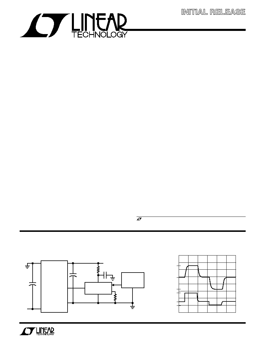
POWER ONE
I5S013ZE-A
+V
IN
+V
OUT
V
OUT
V
IN
1
2
5
6
TRIM
7
SYSTEM
CONTROLLER
THREE-STATE
LTC2920-1
I
M1
GND
R
S1
IN1
R
SET1
10k
1%
2920-1/2 TA01
3.3V
AT 4A
2
µ
F
0.1
µ
F
150
33
µ
F
48V
+
+
3.3V Quarter Brick with
±
5% Voltage Margining
5%
+V
OUT
IN1
1ms/DIV
2920-1/2 TA01a
5%
LOGIC HI
LOGIC FLOAT
LOGIC LOW
NOM
LTC2920-1/LTC2920-2
2
292012i
ORDER PART NUMBER
S5 PART MARKING
T
JMAX
= 125
°
C,
JA
= 250
°
C/W
LTD7
LTD8
LTC2920-1CS5
LTC2920-1IS5
ABSOLUTE AXI U
RATI GS
W
W
W
U
PACKAGE/ORDER I FOR ATIO
U
U
W
(Note 1)
ELECTRICAL CHARACTERISTICS
The
q
denotes the specifications which apply over the full operating
temperature range, otherwise specifications are at T
A
= 25
°
C.
Supply Voltage (V
CC
) ................................ 0.3V to 6.5V
Input Voltages
(IN1, IN2, R
S1
, R
S2
)................. 0.3V to (V
CC
+ 0.3V)
Output Voltages (I
M1
, I
M2
) ........... 0.3V to (V
CC
+ 0.3V)
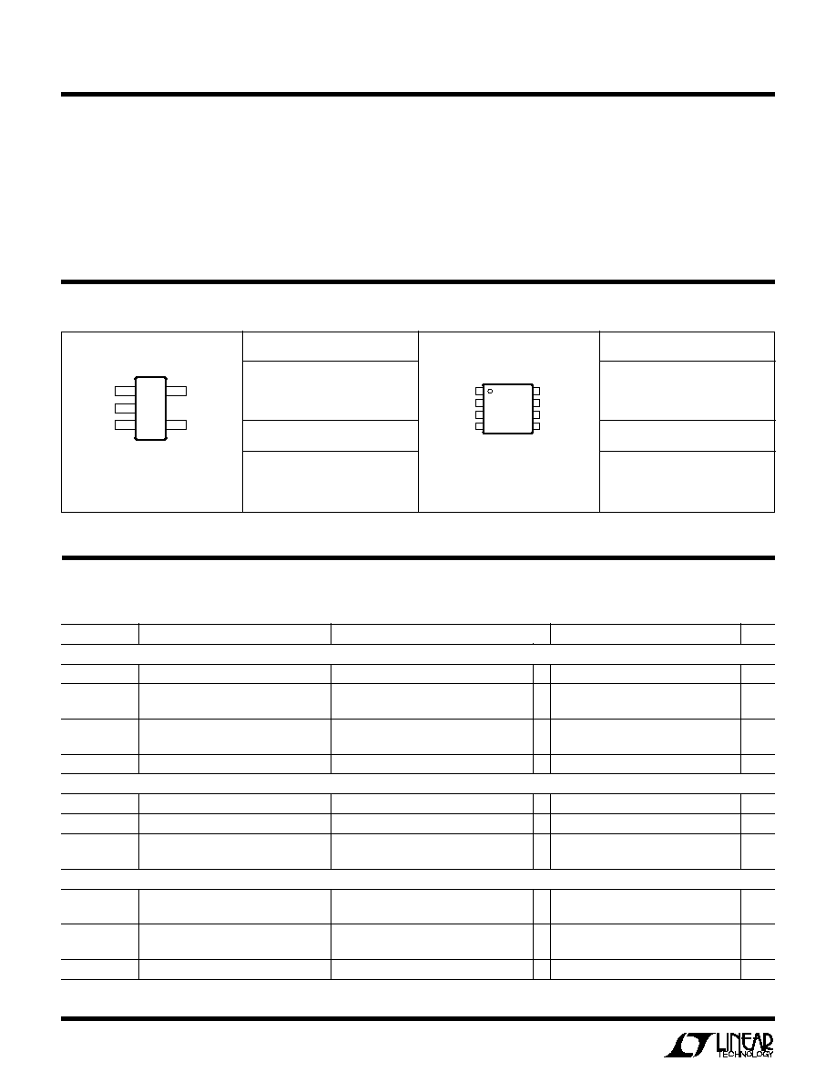
TOP VIEW
S5 PACKAGE
5-LEAD PLASTIC SOT-23
1
2
3
V
CC
GND
I
M1
5
4
IN1
R
S1
ORDER PART NUMBER
MS8 PART MARKING
LTB6
LTA4
LTC2920-2CMS8
LTC2920-2IMS8
T
JMAX
= 125
°
C,
JA
= 200
°
C/W
1
2
3
4
R
S2
IN2
IN1
R
S1
8
7
6
5
V
CC
I
M2
GND
I
M1
TOP VIEW
MS8 PACKAGE
8-LEAD PLASTIC MSOP
Operating Temperature Range
LTC2920-1C/LTC2920-2C ....................... 0
°
C to 70
°
C
LTC2920-1I/LTC2920-2I .................... 40
°
C to 85
°
C
Storage Temperature Range ................. 65
°
C to 150
°
C
Lead Temperature (Soldering, 10 sec).................. 300
°
C
Consult LTC Marketing for parts specified with wider operating temperature ranges.
SYMBOL
PARAMETER
CONDITIONS
MIN
TYP
MAX
UNITS
Supplies
V
CC
Supply Operating Range
(Note 2)
q
2.3
6
V
I
CC(SOURCE)
Supply Current while Sourcing Max I
IM
R
SET1
= R
SET2
= 15k,
q
6
mA
IN1 = IN2 < V
IL
I
CC(Q)
Quiescent Supply Current
R
SET1
= R
SET2
= 200k,
q
0.23
1
mA
IN1 = IN2
V
IL
T
SDJ
Thermal Shutdown Temperature
(Note 5)
145
°
C
Current Setting R
S1
, R
S2
R
SETL
Current Setting Resistor Low Range
q
6
200
k
R
SETH
Current Setting Resistor High Range
q
15
200
k
C
RS
Maximum External Capacitance
Total Capacitance to
20
pF
on R
S1
, R
S2
V
CC
and GND
Current Margining Outputs I
M1
, I
M2
I
IMLOW
Low Range I
MARGIN
Current--
R
SET1
, R
SET2
Tied to GND,
q
5
167
µ
A
Sourcing or Sinking
IN1, IN2 > V
IH
or IN1, IN2 < V
IL
, (Note 4)
I
IMHIGH
High Range I
MARGIN
Current--
R
SET1
, R
SET2
Tied to V
CC
,
q
0.15
2
mA
Sourcing or Sinking
IN1, IN2 > V
IH
or IN1, IN2 < V
IL
, (Note 4)
V
M
I
M1
, I
M2
Output Voltage Compliance
(Note 3)
q
0.55
V
CC
0.55
V
LTC2920-1/LTC2920-2
3
292012i
ELECTRICAL CHARACTERISTICS
The
q
denotes the specifications which apply over the full operating
temperature range, otherwise specifications are at T
A
= 25
°
C.
SYMBOL
PARAMETER
CONDITIONS
MIN
TYP
MAX
UNITS
I
IMACCURACY
Low Range Current Accuracy
100
µ
A
I
M
167
µ
A, (Note 6)
C-Grade
q
3
7.5
%
I-Grade
q
3
13
%
30
µ
A
I
M
< 100
µ
A, (Note 6)
C-Grade
q
5
11
%
I-Grade
q
5
15
%
5
µ
A
I
M
< 30
µ
A, (Note 6)
C-Grade
q
5
20
%
I-Grade
q
5
25
%
High Range Current Accuracy
1.5mA
I
M
2mA, (Note 7)
C-GradeC
q
3
7.5
%
I-Grade
q
3
11
%
600
µ
A
I
M
1.5mA, (Note 7)
C-Grade
q
5
11
%
I-Grade
q
5
15
%
150
µ
A
I
M
600
µ
A, (Note 7)
C-Grade
q
5
15
%
I-Grade
q
5
20
%
I
OZ
I
M1
, I
M2
Leakage Current
q
100
nA
C
IM
Equivalent Capacitance At I
M1
, I
M2
V
IN
= V
OFF
, (Note 5)
10
pF
V
IN
= V
IL
, High Range, (Note 5)
2
nF
V
IN
= V
IL
, Low Range, (Note 5)
30
pF
Control Inputs IN1, IN2
V
IH
Control Voltage for I
M
Current Sinking
V
CC
< 2.5V
q
2.1
V
V
CC
2.5V
q
2.4
V
V
IL
Control Voltage for I
M
Current Sourcing
q
0.6
V
V
OFF
Control Voltage for I
M
Current Off
q
1.1
1.4
V
V
OZ
Control Voltage when Left Floating
1.2
V
R
IN
IN1, IN2 Input Resistance
q
5
12
20
k
I
FLT
Maximum Allowed Leakage at IN1, IN2
q
10
10
µ
A
for I
M
Current Off
Switching Characteristics
V
IN(DELAYON)
I
M1
, I
M2
Turn-On Time
V
IN
Transitions from V
OFF
to
q
15
100
µ
s
V
IH
or V
IL
V
IN(DELAYOFF)
I
M1
, I
M2
Turn-Off Time
V
IN
Transitions from
q
15
100
µ
s
V
IH
or V
IL
to V
OFF
I
M(ON)
I
M1
Rise Time
I
M
5% to 95%, (Note 5)
5
µ
s
I
M(OFF)
I
M1
Fall Time
I
M
95% to 5%, (Note 5)
0.3
µ
s
Note 1: Absolute Maximum Ratings are those values beyond which the life
of a device may be impaired.
Note 2: V
CC
must always be above the maximum of I
M1
and I
M2
less 0.2V.
See Preventing Potential Power Supply Overvoltages in the Applications
Information section.
Note 3: V
M
compliance is the voltage range within which I
M1
and I
M2
are
guaranteed to be sourcing or sinking current. I
M
accuracy will vary within
this range.
Note 4: Consult LTC Marketing for parts specified with wider I
M
current
limits.
Note 5: Determined by design, not production tested.
Note 6:
1 (I
M
R
S
)
· 100%; V
CC
4V: 0.58
V
M
(V
CC
1.1);
V
CC
> 4V: 0.58
V
M
(V
CC
1.4)
Note 7:
1 (I
M
· R
S
/ 30)
· 100%; 0.79
V
M
(V
CC
0.6)

LTC2920-1/LTC2920-2
4
292012i
PI FU CTIO S
U
U
U
V
CC
(Pin 1/Pin 8): Power Supply Input. All internal circuits
are powered from this pin. V
CC
should be connected to a
low noise power supply voltage between 2.2V and 6V and
should be bypassed with at least a 0.1
µ
F capacitor to the
GND pin in close proximity to the LTC2920. Current
sourced out of the I
M
pins comes from the V
CC
pin. Note
that V
CC
must come up no later than the time the
controlled power supply turns on or damage to the load
may result. See Preventing Potential Power Supply Over-
voltages in the Applications Information section for power
sequencing considerations. In certain applications, it may
be necessary to further isolate V
CC
by adding a resistor in
series with its power source. See V
CC
Power Filtering in the
Applications Information section.
GND (Pin 2/Pin 6): Ground. All internal circuits are re-
turned to the GND pin. Connect this ground pin to the
ground of the power supply(s) being margined. Current
sunk into the I
M
pins of the LTC2920 is returned to ground
through this pin.
R
S1
(Pin 4/Pin 4): I
M1
Current Set Input. The R
S1
pin is
used to set the margining current which is sourced or sunk
from the I
M1
pin. The R
S1
pin must be connected to either
V
CC
or ground with an external resistor R
SET
with a value
between 6k and 200k. Connecting R
SET
to ground sets the
current at the I
M1
pin with a multiplier of 1. Connecting
R
SET
to V
CC
sets the current at the I
M1
pin with a multiplier
of 30. If R
SET
is connected to ground,
1V will appear at the
R
S1
pin. If R
SET
is connected to V
CC
,
(V
CC
1V) will
appear at the R
S1
pin. In either case, the current through
R
SET
will be
1V/R
SET
.
(S5 Package/MS8 Package)
I
M1
(Pin 3/Pin 5): I
M1
Current Output. This pin should be
connected to the power supply feedback pin or voltage
adjust pin. (See the Applications Information section for
further details.) Current is either sourced out of or sunk
into this pin. The direction of the current is controlled by
the IN1 pin. The amount of current flowing into or out of
the I
M1
pin is controlled by the R
S1
pin.
IN1 (Pin 5/Pin 3): I
M1
Control Pin. This pin is a 3-level input
pin which controls the I
M1
pin. If the IN1 pin is pulled above
2V, current is sunk into the I
M1
pin. If the IN1 pin is pulled
below 0.6V, current is sourced from the I
M1
pin. If the IN1
pin is left floating, or held between 1.1V and 1.4V, the I
M1
pin is a high impedance output. Internally, the IN1 pin is
connected to a 1.2V voltage source by an internal ~10k
resistor. The LTC2920 has an internal RC circuit to sup-
press noise entering from this pin.
LTC2920-2 Only
R
S2
(NA/Pin 1): I
M2
Current Set Input. Sets the current for
I
M2
. See R
S1
.
I
M2
(NA/Pin 7): I
M2
Current Output. This pin is the second
margin current output for the LTC2920. See I
M1
.
IN2 (NA/Pin 2): I
M2
Control Pin. This pin controls the
current at the I
M2
pin. See IN1.
LTC2920-1/LTC2920-2
5
292012i
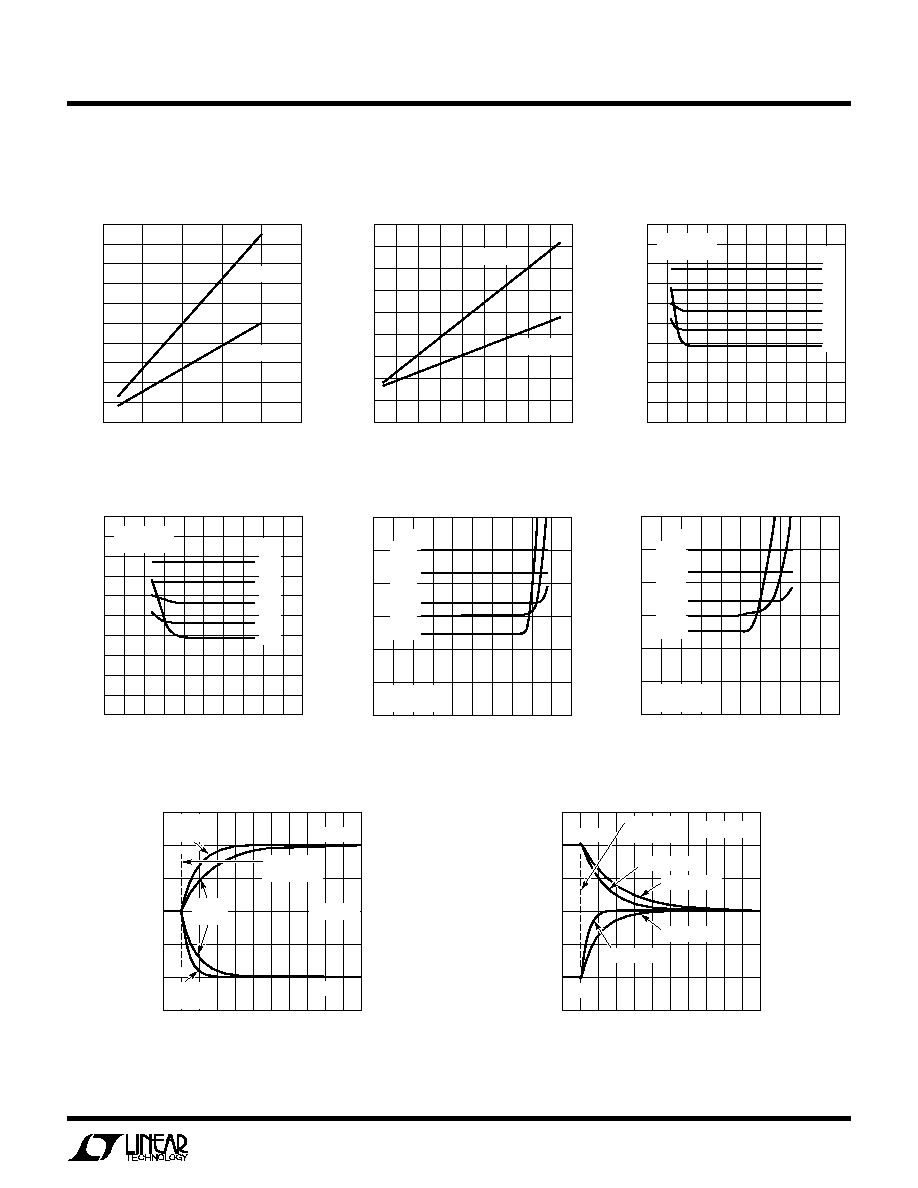
TYPICAL PERFOR A CE CHARACTERISTICS
U
W
I
MARGIN
(mA)
0
0.5
1
1.5
2
2.5
I
CC
(mA)
2920-1/2 G01
5.0
4.5
4.0
3.5
3.0
2.5
2.0
1.5
1.0
0.5
0
1 CHANNEL
2 CHANNELS
I
MARGIN
(
µ
A)
0
20
40
60
80 100 120 140 160 180
I
CC
(
µ
A)
2920-1/2 G02
1800
1600
1400
1200
1000
800
600
400
200
0
1 CHANNEL
2 CHANNELS
V
MARGIN
(V)
0
0.5
1
1.5
2
2.5
3
3.5
4
4.5
5
ERROR (%)
2920-1/2 G03
5.0
4.5
4.0
3.5
3.0
2.5
2.0
1.5
1.0
0.5
0
0.15
(mA)
0.3
0.5
1
2
V
CC
= 5V
HIGH RANGE
V
MARGIN
(V)
0
0.5
1
1.5
2
2.5
ERROR (%)
2920-1/2 G04
5.0
4.5
4.0
3.5
3.0
2.5
2.0
1.5
1.0
0.5
0
0.15
(mA)
0.3
0.5
1
2
V
CC
= 2.5V
HIGH RANGE
0
0.5
1
1.5
2
2.5
3
3.5
4
4.5
5
V
MARGIN
(V)
ERROR (%)
2920-1/2 G05
6
5
4
3
2
1
0
5
(
µ
A)
20
50
166.7
100
V
CC
= 5V
LOW RANGE
V
MARGIN
(V)
0
0.5
1
1.5
2
2.5
ERROR (%)
2920-1/2 G06
6
5
4
3
2
1
0
5
(
µ
A)
20
50
166.7
100
V
CC
= 2.5V
LOW RANGE
I
CC
vs I
MARGIN
High Range
Sourcing Current
I
CC
vs I
MARGIN
Low Range
Sourcing Current
I
MARGIN
Error vs V
MARGIN
I
MARGIN
Error vs V
MARGIN
I
MARGIN
Error vs V
MARGIN
I
MARGIN
Error vs V
MARGIN
2920-1/2 G07
100%
100%
SOURCE
R
SET
= 20k
0%
SINK
1
µ
s/DIV
HIGH
RANGE
V
IN(DELAYON)
ENDS
HIGH
RANGE
LOW
RANGE
2920-1/2 G08
100%
100%
R
SET
= 20k
0%
100ns/DIV
HIGH RANGE
LOW RANGE
HIGH RANGE
LOW RANGE
SOURCE
SINK
V
IN(DELAYOFF)
ENDS
I
MARGIN
Rise Time
I
MARGIN
Fall Time