Äîêóìåíòàöèÿ è îïèñàíèÿ www.docs.chipfind.ru
1
LT1785/LT1785A
LT1791/LT1791A
60V Fault Protected
RS485/RS422 Transceivers
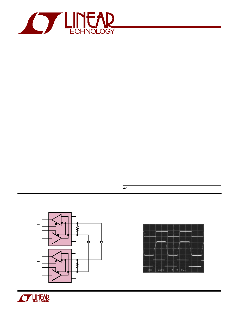
Normal Operation Waveforms at 250kBaud
GND1
GND2
R
TERM
1785/91 TA01
RO1
RE1
DE1
DI1
LT1785
RO2
RE2
DE2
DI2
LT1785
V
CC1
V
CC2
R
TERM
TX
TX
RX
RX
DESCRIPTIO
U
The LT
®
1785/LT1791 are half-duplex and full-duplex dif-
ferential bus transceivers for RS485 and RS422 applica-
tions which feature on-chip protection from overvoltage
faults on the data transmission lines. Receiver input and
driver output pins can withstand voltage faults up to
±
60V
with respect to ground with no damage to the device.
Faults may occur while the transceiver is active, shut down
or powered off.
Data rates to 250kbaud on networks of up to 128 nodes are
supported. Controlled slew rates on the driver outputs
control EMI emissions and improve data transmission
integrity on improperly terminated lines. Drivers are speci-
fied to operate with inexpensive cables as low as 72
characteristic impedance.
The LT1785A/LT1791A devices have "fail-safe" receiver
inputs to guarantee a receiver output high for shorted,
open or inactive data lines. On-chip ESD protection elimi-
nates need for external protection devices.
The LT1785/LT1785A are available in 8-lead DIP and SO
packages and the LT1791/LT1791A in 14-lead DIP and SO
packages.
s
Protected from Overvoltage Line Faults to
±
60V
s
Pin Compatible with LTC485 and LTC491
s
High Input Impedance Supports Up to 128 Nodes
s
No Damage or Latchup to ESD
IEC-1000-4-2 Level 4:
±
15kV Air Discharge
IEC-1000-4-2 Level 2:
±
4kV Contact Discharge
s
Controlled Slew Rates for EMI Emissions Control
s
Guaranteed High Receiver Output State for Floating,
Shorted or Inactive Inputs
s
Outputs Assume a High Impedance When Off or
Powered Down
s
Drives Low Cost, Low Impedance Cables
s
Short-Circuit Protection on All Outputs
s
Thermal Shutdown Protection
s
Industrial Control Data Networks
s
CAN Bus Applications
s
HVAC Controls
1785/91 TA02
, LTC and LT are registered trademarks of Linear Technology Corporation.
FEATURES
APPLICATIO S
U
TYPICAL APPLICATIO
U
RO
Y-Z
DI
2
LT1785/LT1785A
LT1791/LT1791A
A
U
G
W
A
W
U
W
A
R
BSOLUTE
XI
TI
S
(Note 1)
Operating Temperature Range
LT1785C/LT1791C/
LT1785AC/LT1791AC ............................. 0
°
C to 70
°
C
LT1785I/LT1791I ............................... 40
°
C to 85
°
C
Storage Temperature Range ................ 65
°
C to 150
°
C
Lead Temperature (Soldering, 10 sec)................. 300
°
C
Supply Voltage (V
CC
) .............................................. 18V
Receiver Enable Input Voltage .................... 0.3V to 6V
Driver Enable Input Voltage ........................ 0.3V to 6V
Driver Input Voltage .................................. 0.3V to 18V
Receiver Input Voltage ............................... 60V to 60V
Driver Output Voltage ............................... 60V to 60V
Receiver Output Voltage ................ 0.3V to (V
CC
+ 6V)
W
U
U
PACKAGE/ORDER I FOR ATIO
ORDER PART
NUMBER
LT1791CN
LT1791CS
LT1791IN
LT1791IS
LT1791ACN
LT1791ACS
ORDER PART
NUMBER
LT1785CN8
LT1785CS8
LT1785IN8
LT1785IS8
LT1785ACN8
LT1785ACS8
T
JMAX
= 150
°
C,
JA
= 130
°
C/ W (N8)
T
JMAX
= 150
°
C,
JA
= 150
°
C/ W (S8)
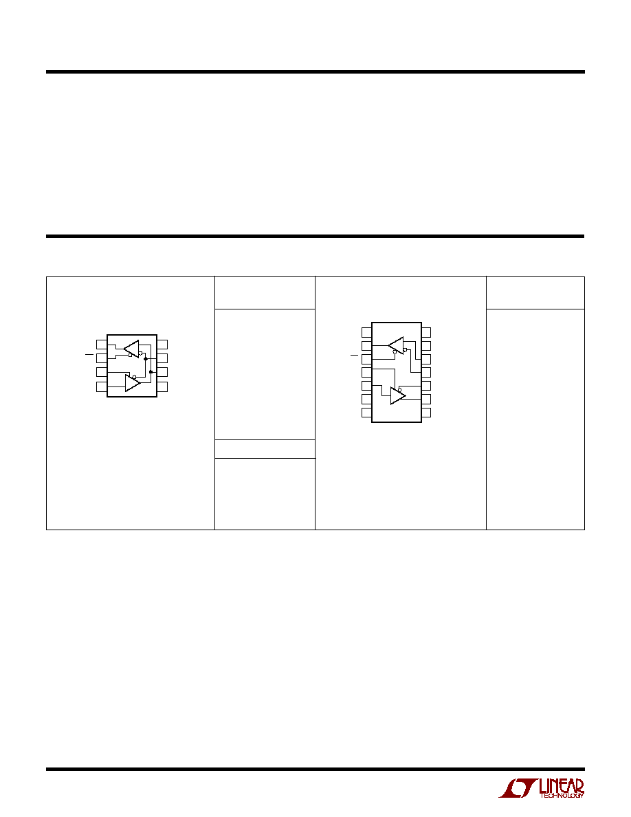
1
2
3
4
8
7
6
5
TOP VIEW
V
CC
B
A
GND
N8 PACKAGE
8-LEAD PDIP
S8 PACKAGE
8-LEAD PLASTIC SO
R
D
RO
RE
DE
DI
TOP VIEW
N PACKAGE
14-LEAD PDIP
S PACKAGE
14-LEAD PLASTIC SO
1
2
3
4
5
6
7
14
13
12
11
10
9
8
NC
RO
RE
DE
DI
GND
GND
V
CC
NC
A
B
Z
Y
NC
R
D
T
JMAX
= 150
°
C,
JA
= 130
°
C/ W (N)
T
JMAX
= 150
°
C,
JA
= 150
°
C/ W (S)
S8 PART MARKING
1785
1785I
1785A
Consult factory for Military grade parts.
3
LT1785/LT1785A
LT1791/LT1791A
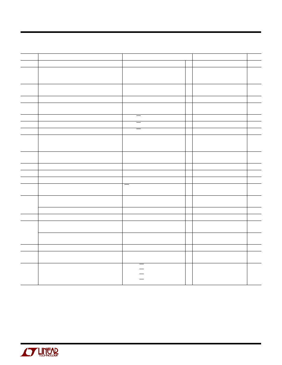
DC ELECTRICAL CHARACTERISTICS
SYMBOL
PARAMETER
CONDITIONS
MIN
TYP
MAX
UNITS
V
OD1
Differential Driver Output Voltage (Unloaded)
I
O
= 0
q
4.1
5
V
V
OD2
Differential Driver Output Voltage (With Load)
R = 50
(RS422), Figure 1
q
2.0
2.70
V
R = 27
(RS485), Figure 1
q
1.5
2.45
V
R = 18
q
1.2
2.2
V
V
OD
Change in Magnitude of Driver Differential Output
R = 27
or R = 50
, Figure 1
q
0.2
V
Voltage for Complementary Output States
V
OC
Driver Common Mode Output Voltage
R = 27
or R = 50
, Figure 1
q
2
2.5
3
V
V
OC
Change in Magnitude of Driver Common Mode
R = 27
or R = 50
, Figure 1
q
0.2
V
Output Voltage for Complementary Output States
V
IH
Input High Voltage
DI, DE, RE
q
2
V
V
IL
Input Low Voltage
DI, DE, RE
q
0.8
V
I
IN1
Input Current
DI, DE, RE
q
5
µ
A
I
IN2
Input Current (A, B); (LT1791 or LT1785 with
V
IN
= 12V
q
0.15
0.3
mA
DE = 0V)
V
IN
= 7V
q
0.15
0.08
mA
60V
V
IN
60V
q
6
6
mA
V
TH
Differential Input Threshold Voltage for Receiver
LT1785/LT1791: 7V
V
CM
12V
q
0.2
0.2
V
LT1785A/LT1791A: 7V
V
CM
12V
q
0.2
0
V
V
TH
Receiver Input Hysteresis
7V < V
CM
< 12V
20
mV
V
OH
Receiver Output High Voltage
I
O
= 400
µ
A, V
ID
= 200mV
q
3.5
4
V
V
OL
Receiver Output Low Voltage
I
O
= 1.6mA, V
ID
= 200mV
q
0.3
0.5
V
Three-State (High Impedance) Output Current
RE > 2V or Power Off
q
1
1
µ
A
at Receiver 0V < V
OUT
< 6V
R
IN
Receiver Input Resistance (LT1791)
7V
V
CM
12V
q
85
125
k
60V
V
CM
60V
125
k
LT1785
7V
V
CM
12V
q
50
90
k
RS485 Unit Load
0.25
I
SC
Driver Short-Circuit Current
V
OUT
= HIGH, Force V
O
= 7V
q
35
250
mA
V
OUT
= LOW, Force V
O
= 12V
q
35
250
mA
Driver Output Fault Current
V
O
= 60V
q
6
mA
V
O
= 60V
q
6
mA
Receiver Short-Circuit Current
0V
V
O
V
CC
q
±
30
mA
Driver Three-State Output Current
7V
V
O
12V
q
0.2
0.3
mA
60V
V
O
60V
q
6
6
mA
I
CC
Supply Current
No Load, RE = 0V, DE = 5V
q
5.5
9
mA
No Load, RE = 5V, DE = 5V
q
5.5
9
mA
No Load, RE = 0V, DE = 0V
q
4.5
8
mA
No Load, RE = 5V, DE = 0V
q
0.2
0.3
mA
The
q
denotes specifications which apply over the full operating temperature range, otherwise specifications are TA = 25
°
C, V
CC
= 5V.
4
LT1785/LT1785A
LT1791/LT1791A
SWITCHI G CHARACTERISTICS
U
SYMBOL
PARAMETER
CONDITIONS
MIN
TYP
MAX
UNITS
t
PLH
Driver Input to Output
Figures 3, 5
q
700
2000
ns
t
PHL
Driver Input to Output
Figures 3, 5
q
700
2000
ns
t
SKEW
Driver Output to Output
Figures 3, 5
100
ns
t
r
, t
f
Driver Rise or Fall Time
Figures 3, 5
q
200
800
2000
ns
t
ZH
Driver Enable to Output High
Figures 4, 6
q
500
3000
ns
t
ZL
Driver Enable to Output Low
Figures 4, 6
q
800
3000
ns
t
LZ
Driver Disable Time from Low
Figures 4, 6
q
200
5000
ns
t
HZ
Driver Disable Time from High
Figures 4, 6
q
800
5000
ns
t
PLH
Receiver Input to Output
Figures 3, 7
q
400
900
ns
t
PHL
Receiver Input to Output
Figures 3, 7
q
400
900
ns
t
SKD
Differential Receiver Skew
200
ns
t
ZL
Receiver Enable to Output Low
Figures 2, 8
q
300
1000
ns
t
ZH
Receiver Enable to Output High
Figures 2, 8
q
300
1000
ns
t
LZ
Receiver Disable from Low
Figures 2, 8
q
400
1000
ns
t
HZ
Receiver Disable from High
Figures 2, 8
q
400
1000
ns
f
MAX
Maximum Data Rate
q
250
kbps
t
SHDN
Time to Shut Down
Figures 2, 6, 8
3
µ
s
t
ZH(SHDN)
Driver Enable from Shutdown to Output High
Figures 2, 6; RE = 5V
12
µ
s
t
ZL(SHDN)
Driver Enable from Shutdown to Output Low
Figures 2, 6; RE = 5V
12
µ
s
t
ZH(SHDN)
Receiver Enable from Shutdown to Output High
Figures 2, 8; DE = 0V
4
µ
s
t
ZL(SHDN)
Receiver Enable from Shutdown to Output Low
Figures 2, 8; DE = 0V
4
µ
s
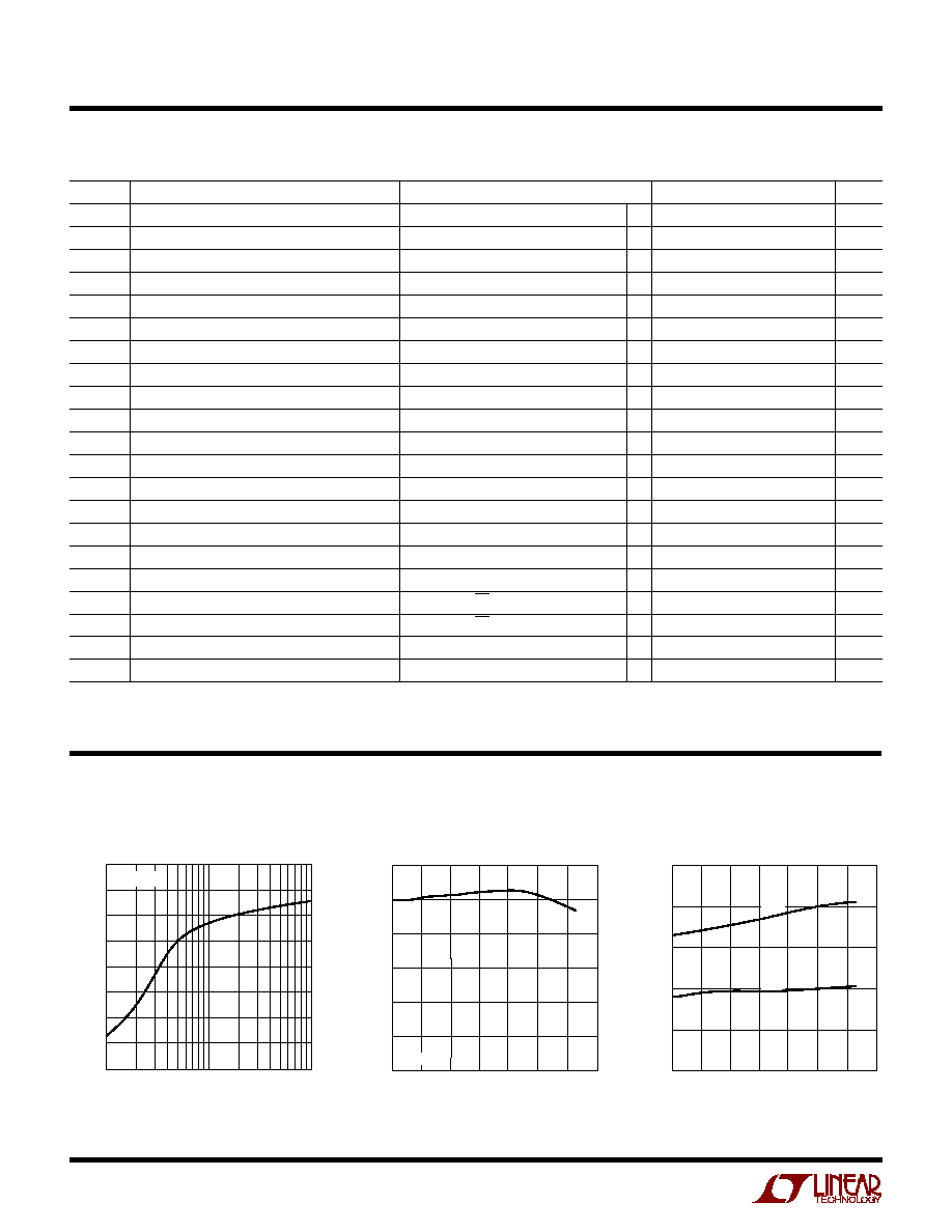
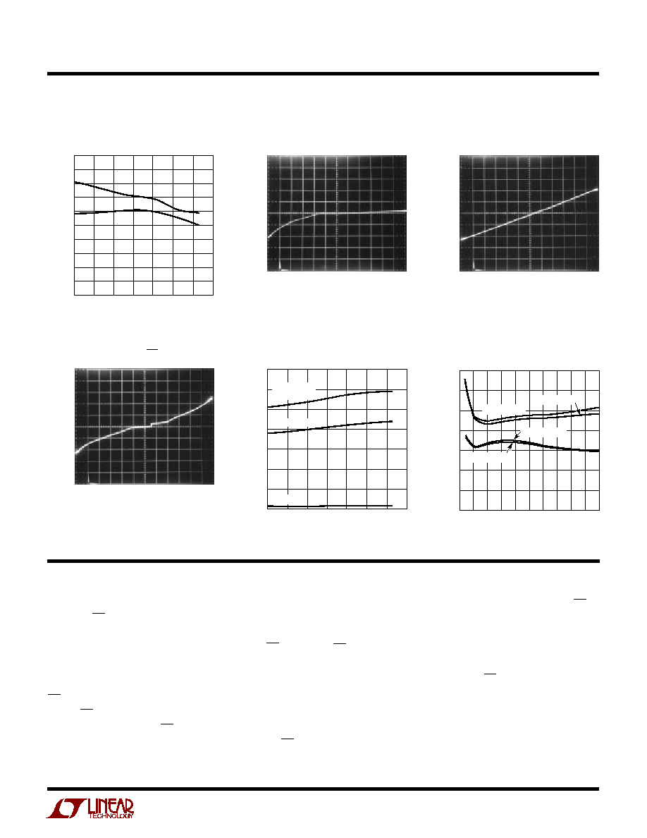
TYPICAL PERFOR
M
A
N
CE CHARACTERISTICS
U
W
Note 1: Absolute Maximum Ratings are those values beyond which the life
of a device may be impaired.
LOAD RESISTANCE (
)
10
OUTPUT VOLTAGE (V)
4
3
2
1
0
100
1k
1785/91 G01
T
A
= 25
°
C
Driver Differential Output Voltage
vs Load Resistance
TEMPERATURE (
°
C)
40
DELAY (ns)
1000
800
600
400
200
0
0
40
60
1785/91 G03
20
20
80
100
t
PLH
t
PHL
Receiver Propagation Delay
vs Temperature
TEMPERATURE (
°
C)
40
DIFFERENTIAL VOLTAGE (V)
3.0
2.5
2.0
1.5
1.0
0.5
0
0
40
60
1785/91 G03
20
20
80
100
R = 27
Driver Differential Output Voltage
vs Temperature
The
q
denotes specifications which apply over the full operating temperature range, otherwise specifications are TA = 25
°
C, V
CC
= 5V.
5
LT1785/LT1785A
LT1791/LT1791A
TYPICAL PERFOR
M
A
N
CE CHARACTERISTICS
U
W
Supply Current vs Temperature
Driver Propagation Delay
vs Temperature
LT1791 Driver Output Leakage
DE = 0V
TEMPERATURE (
°
C)
40
PROPAGATION DELAY (ns)
1000
900
800
700
600
500
400
300
200
100
0
0
40
60
1785/91 G04
20
20
80
100
HL
LH
1mA/DIV
60V
60V
LT1791 Receiver Input Current
vs V
IN
200
µ
A/DIV
60V
60V
V
IN
1785/91 G06
60V
60V
1mA/DIV
V
A,
V
B
1785/91 G07
V
OUT
1785/91 G05
TEMPERATURE (
°
C)
40
I
CC
(mA)
7
6
5
4
3
2
1
0
0
40
60
1785/91 G08
20
20
80
100
RECEIVER ONLY
STANDBY
DRIVER AND
RECEIVER ON
Receiver Propagation Delay
vs Differential Input Voltage
LT1785 Input Characteristics
Pins A or B; DE = RE = 0V
V
IN
DIFFERENTIAL (V)
0
DELAY (ns)
700
600
500
400
300
200
100
0
1785/91 G09
2
5
1
3
4
HL V
CM
= 12V
HL V
CM
= 7V
LH V
CM
= 7V
LH V
CM
= 12V
PI
N
FU
N
CTIO
N
S
U
U
U
RO: Receiver Output. TTL level logic output. If the receiver
is active (RE pin low), RO is high if receiver input A
B by
200mV. If A
B by 200mV, then RO will be low. RO
assumes a high impedance output state when RE is high
or the part is powered off. RO is protected from output
shorts from ground to 6V.
RE: Receiver Output Enable. TTL level logic input. A logic
low on RE enables normal operation of the receiver output
RO. A logic high level at RE places the receiver output pin
RO into a high impedance state. If receiver enable RE and
driver enable DE are both in the disable state, the circuit
goes to a low power shutdown state. Placing either RE or
DE into its active state brings the circuit out of shutdown.
Shutdown state is not entered until a 3
µ
s delay after both
RE and DE are disabled, allowing for logic skews in
toggling between transmit and receive modes of opera-
tion. For CAN bus applications, RE should be tied low to
prevent the circuit from entering shutdown.
DE: Driver Output Enable. TTL level logic input. A logic
high on DE enables normal operation of the driver outputs
(Y and Z on LT1791, A and B on LT1785). A logic low level
at DE places the driver output pins into a high impedance