Äîêóìåíòàöèÿ è îïèñàíèÿ www.docs.chipfind.ru
Integrated
Circuit
Systems, Inc.
General Description
Features
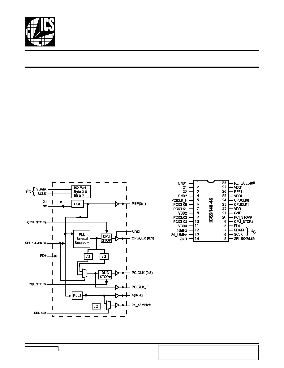
ICS9148-46
Block Diagram
Pentium/Pro
TM
System Clock Chip
9148-46 Rev E 4/20/99
Pin Configuration
28 pin SSOP
Pentium is a trademark on Intel Corporation.
Generates system clocks for CPU, PCI, 14.314 MHz,
48 and 24MHz.
Supports single or dual processor systems
Skew from CPU (earlier) to PCI clock 1 to 4ns
Separate 2.5V and 3.3V supply pins
2.5V outputs: CPU
3.3V outputs: PCI, REF
No power supply sequence requirements
28 pin SSOP
Spread Sectrum operation optional for PLL1
CPU frequencies to 100MHz are supported.
The ICS9148-46 is part of a reduced pin count two-chip clock
solution for designs using an Intel BX style chipset.
Companion SDRAM buffers are ICS9179-03, and -12.
There are two PLLs, with the first PLL capable of spread
spectrum operation. Spread spectrum typically reduces system
EMI by 8-10dB. The second PLL provides support for USB
(48MHz) and 24MHz requirements. CPU frequencies up to
100MHz are supported.
The I
2
C interface allows stop clock programming, frequency
selection, and spread spectrum operation to be programmed.
Clock outputs include two CPU (2.5V or 3.3V), five PCI (3.3V),
two REF (3.3V), one 48MHz, and one selectable 48_24MHz.
Ground Groups
GND = Ground Source Core, CPUCLK (0:1)
GND1 = REF(0:1), X1, X2
GND2 = PCICLK_F, PCICLK (0:5)
GND3=48MHz, 24/48MHz
Power Groups
VDD = Supply for PLL core
VDD1 = REF(0:1), X1, X2
VDD2 = PCICLK_F, PCICLK (0:3)
VDD3 = 48MHz, 24/48MHz
VDDL = CPUCLK (0:1)
ICS reserves the right to make changes in the device data identified in
this publication without further notice. ICS advises its customers to
obtain the latest version of all device data to verify that any
information being relied upon by the customer is current and accurate.
2
ICS9148-46
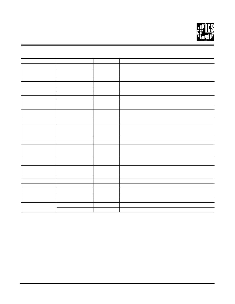
Pin Descriptions
R
E
B
M
U
N
N
I
P
E
M
A
N
N
I
P
E
P
Y
T
N
O
I
T
P
I
R
C
S
E
D
1
1
D
N
G
R
W
P
.
2
X
,
1
X
,
)
1
:
0
(
F
E
R
r
o
f
d
n
u
o
r
G
2
1
X
N
I
F
p
3
3
l
a
n
r
e
t
n
i
s
a
h
,
t
u
p
n
i
l
a
t
s
y
r
C
z
H
M
8
1
3
.
4
1
N
I
_
L
A
T
X
2
X
m
o
r
f
r
o
t
s
i
s
e
r
k
c
a
b
d
e
e
f
d
n
a
p
a
c
d
a
o
l
3
2
X
T
U
O
F
p
3
3
p
a
c
d
a
o
l
l
a
n
r
e
t
n
i
s
a
h
,
t
u
p
t
u
o
l
a
t
s
y
r
C
T
U
O
_
L
A
T
X
4
2
D
N
G
R
W
P
s
t
u
p
t
u
o
I
C
P
r
o
f
d
n
u
o
r
G
5
F
_
K
L
C
I
C
P
T
U
O
#
P
O
T
S
_
I
C
P
y
b
d
e
t
c
e
f
f
a
t
o
N
.
t
u
p
t
u
o
I
C
P
g
n
i
n
n
u
R
e
e
r
F
0
1
,
9
,
7
,
6
)
3
:
0
(
K
L
C
I
C
P
T
U
O
V
3
.
3
e
l
b
i
t
a
p
m
o
c
L
T
T
.
s
t
u
p
t
u
o
k
c
o
l
c
I
C
P
8
2
D
D
V
R
W
P
V
3
.
3
y
l
l
a
n
i
m
o
n
,
s
t
u
p
t
u
o
K
L
C
I
C
P
r
o
f
r
e
w
o
P
1
1
3
D
D
V
R
W
P
z
H
M
8
4
r
o
f
r
e
o
P
2
1
z
H
M
8
4
T
U
O
z
H
M
8
4
@
t
u
p
t
u
o
K
L
C
d
e
x
i
F
3
1
z
H
M
8
4
_
4
2
T
U
O
,
p
u
r
e
w
o
p
t
a
1
=
7
2
n
i
p
f
i
z
H
M
4
2
;
t
u
p
t
u
o
K
L
C
d
e
x
i
F
.
p
u
r
e
w
o
p
t
a
0
=
7
2
n
i
p
f
i
z
H
M
8
4
4
1
3
D
N
G
R
W
P
z
H
M
8
4
r
o
f
d
n
u
o
r
G
5
1
#
6
.
6
6
/
0
0
1
L
E
S
N
I
z
H
M
6
.
6
6
r
o
z
H
M
0
0
1
g
n
i
l
b
a
n
e
r
o
f
n
i
p
t
c
e
l
e
S
s
u
o
n
o
r
h
c
n
y
s
s
y
a
w
l
a
I
C
P
(
z
H
M
6
.
6
6
=
L
,
z
H
M
0
0
1
=
H
)
z
H
M
3
.
3
3
6
1
K
L
C
S
N
I
I
r
o
f
t
u
p
n
i
k
c
o
l
C
2
t
u
p
n
i
C
7
1
A
T
A
D
S
N
I
I
r
o
f
t
u
p
n
i
a
t
a
D
2
t
u
p
n
i
C
8
1
#
D
P
N
I
s
e
l
b
a
s
i
d
)
W
O
L
(
e
v
i
t
c
a
n
e
v
i
r
d
n
e
h
w
t
u
p
n
i
s
u
o
n
o
r
h
c
n
y
s
A
d
e
c
a
l
p
e
r
a
s
t
u
p
t
u
o
l
l
A
.
y
l
r
a
e
O
C
V
s
p
o
t
s
,
s
k
c
o
l
c
l
a
n
r
e
t
n
i
.
e
l
c
y
c
t
n
e
r
u
c
e
h
t
f
o
d
n
e
e
h
t
t
a
e
t
a
t
s
W
O
L
a
n
i
9
1
#
P
O
T
S
_
U
P
C
N
I
s
p
o
t
s
)
W
O
L
(
e
v
i
t
c
a
n
e
v
i
r
d
n
e
h
w
t
u
p
n
i
s
u
o
n
o
r
h
c
n
y
s
A
.
e
t
a
t
s
W
O
L
a
n
i
)
1
:
0
(
K
L
C
U
P
C
0
2
#
P
O
T
S
_
I
C
P
N
I
s
p
o
t
s
)
W
O
L
(
e
v
i
t
c
a
n
e
v
i
r
d
n
e
h
w
t
u
p
n
i
s
u
o
n
o
r
h
c
n
y
s
A
.
d
e
t
c
e
f
f
a
t
o
n
s
i
F
_
K
L
C
I
C
P
.
e
t
a
t
s
W
O
L
a
n
i
)
3
:
0
(
K
L
C
I
C
P
1
2
D
N
G
R
W
P
e
r
o
c
e
h
t
d
n
a
)
1
:
0
(
K
L
C
U
P
C
r
o
f
d
n
u
o
r
G
2
2
D
D
V
R
W
P
e
r
o
c
L
L
P
r
o
f
r
e
w
o
P
4
2
,
3
2
)
0
:
1
(
K
L
C
U
P
C
T
U
O
V
5
.
2
y
l
l
a
n
i
m
o
n
s
t
u
p
t
u
o
k
c
o
l
c
t
s
o
H
d
n
a
U
P
C
5
2
L
D
D
V
R
W
P
V
5
.
2
y
l
l
a
n
i
m
o
n
,
s
t
u
p
t
u
o
U
P
C
r
o
f
r
e
w
o
P
6
2
1
F
E
R
T
U
O
t
u
p
t
u
o
k
c
o
l
c
e
c
n
e
r
e
f
e
R
z
H
M
8
1
3
.
4
1
7
2
1
D
D
V
R
W
P
.
s
t
u
p
t
u
o
F
E
R
r
o
f
r
e
w
o
P
8
2
0
F
E
R
T
U
O
t
u
p
t
u
o
k
c
o
l
c
z
H
M
8
1
3
.
4
1
#
8
4
L
E
S
N
I
.
z
H
M
8
4
s
i
3
1
n
i
p
,
w
o
l
n
e
h
W
.
p
u
r
e
w
o
p
t
a
t
u
p
n
i
d
e
h
c
t
a
L
3
ICS9148-46
1.
The ICS clock generator is a slave/receiver, I
2
C component. It can read back the data stored in the latches for verification.
Read-Back will support Intel PIIX4 "Block-Read" protocol.
2.
The data transfer rate supported by this clock generator is 100K bits/sec or less (standard mode)
3.
The input is operating at 3.3V logic levels.
4.
The data byte format is 8 bit bytes.
5.
To simplify the clock generator I
2
C interface, the protocol is set to use only "Block-Writes" from the controller. The
bytes must be accessed in sequential order from lowest to highest byte with the ability to stop after any complete byte
has been transferred. The Command code and Byte count shown above must be sent, but the data is ignored for those
two bytes. The data is loaded until a Stop sequence is issued.
6.
At power-on, all registers are set to a default condition, as shown.
General I
2
C serial interface information
The information in this section assumes familiarity with I
2
C programming.
For more information, contact ICS for an I
2
C programming application note.
How to Write:
Controller (host) sends a start bit.
Controller (host) sends the write address D2
(H)
ICS clock will acknowledge
Controller (host) sends a dummy command code
ICS clock will acknowledge
Controller (host) sends a dummy byte count
ICS clock will acknowledge
Controller (host) starts sending first byte (Byte 0)
through byte 5
ICS clock will acknowledge each byte one at a time.
Controller (host) sends a Stop bit
How to Read:
Controller (host) will send start bit.
Controler (host) sends the read address D3
(H)
ICS clock will acknowledge
ICS clock will send the byte count
Controller (host) acknowledges
ICS clock sends first byte (Byte 0) through byte 6
Controller (host) will need to acknowledge each byte
Controller (host) will send a stop bit
Notes:
Controller (Host)
ICS (Slave/Receiver)
Start Bit
Address
D2
(H)
ACK
Dummy Command Code
ACK
Dummy Byte Count
ACK
Byte 0
ACK
Byte 1
ACK
Byte 2
ACK
Byte 3
ACK
Byte 4
ACK
Byte 5
ACK
Byte 6
ACK
Stop Bit
How to Write:
Controller (Host)
ICS (Slave/Receiver)
Start Bit
Address
D3
(H)
ACK
Byte Count
ACK
Byte 0
ACK
Byte 1
ACK
Byte 2
ACK
Byte 3
ACK
Byte 4
ACK
Byte 5
ACK
Byte 6
ACK
Stop Bit
How to Read:
4
ICS9148-46
Note: PWD = Power-Up Default
Byte 3: Functionality & Frequency Select
& Spread Slect Register
Notes: 1 = Enabled; 0 = Disabled, outputs held low
Byte 4:
Notes: 1 = Enabled; 0 = Disabled, outputs held low
t
i
B
#
n
i
P
e
m
a
N
n
i
P
D
W
P
n
o
i
t
p
i
r
c
s
e
D
0
=
e
u
l
a
V
t
i
B
1
=
e
u
l
a
V
t
i
B
7
-
-
-
)
d
e
v
r
e
s
e
R
(
)
d
e
v
r
e
s
e
R
(
6
-
-
-
)
d
e
v
r
e
s
e
R
(
)
d
e
v
r
e
s
e
R
(
5
-
-
-
)
d
e
v
r
e
s
e
R
(
)
d
e
v
r
e
s
e
R
(
4
-
-
-
)
d
e
v
r
e
s
e
R
(
)
d
e
v
r
e
s
e
R
(
3
-
-
-
)
d
e
v
r
e
s
e
R
(
)
d
e
v
r
e
s
e
R
(
2
3
2
1
K
L
C
U
P
C
1
d
e
l
b
a
s
i
D
)
w
o
l
(
d
e
l
b
a
n
E
1
-
-
0
)
d
e
v
r
e
s
e
R
(
)
d
e
v
r
e
s
e
R
(
0
4
2
0
K
L
C
U
P
C
1
)
d
e
l
b
a
s
i
D
(
)
w
o
l
(
d
e
l
b
a
n
E
Byte 5:
Notes: 1 = Enabled; 0 = Disabled, outputs held low
t
i
B
#
n
i
P
e
m
a
N
n
i
P
D
W
P
n
o
i
t
p
i
r
c
s
e
D
0
=
e
u
l
a
V
t
i
B
1
=
e
u
l
a
V
t
i
B
7
5
F
_
K
L
C
I
C
P
1
d
e
l
b
a
s
i
D
)
w
o
l
(
d
e
l
b
a
n
E
6
0
1
3
K
L
C
I
C
P
1
d
e
l
b
a
s
i
D
)
w
o
l
(
d
e
l
b
a
n
E
5
9
2
K
L
C
I
C
P
1
d
e
l
b
a
s
i
D
)
w
o
l
(
d
e
l
b
a
n
E
4
-
-
0
)
d
e
v
r
e
s
e
R
(
)
d
e
v
r
e
s
e
R
(
3
7
1
K
L
C
I
C
P
1
d
e
l
b
a
s
i
D
)
w
o
l
(
d
e
l
b
a
n
E
2
6
0
K
L
C
I
C
P
1
d
e
l
b
a
s
i
D
)
w
o
l
(
d
e
l
b
a
n
E
1
-
-
0
)
d
e
v
r
e
s
e
R
(
)
d
e
v
r
e
s
e
R
(
0
-
-
0
)
d
e
v
r
e
s
e
R
(
)
d
e
v
r
e
s
e
R
(
Byte 6:
Notes: 1 = Enabled; 0 = Disabled, outputs held low
t
i
B
#
n
i
P
e
m
a
N
n
i
P
D
W
P
n
o
i
t
p
i
r
c
s
e
D
0
=
e
u
l
a
V
t
i
B
1
=
e
u
l
a
V
t
i
B
7
-
-
0
)
d
e
v
r
e
s
e
R
(
)
d
e
v
r
e
s
e
R
(
6
-
-
0
)
d
e
v
r
e
s
e
R
(
)
d
e
v
r
e
s
e
R
(
5
-
-
0
)
d
e
v
r
e
s
e
R
(
)
d
e
v
r
e
s
e
R
(
4
-
-
0
)
d
e
v
r
e
s
e
R
(
)
d
e
v
r
e
s
e
R
(
3
-
-
0
)
d
e
v
r
e
s
e
R
(
)
d
e
v
r
e
s
e
R
(
2
6
2
1
F
E
R
1
)
d
e
l
b
a
s
i
D
(
)
w
o
l
(
d
e
l
b
a
n
E
1
-
-
0
)
d
e
v
r
e
s
e
R
(
)
d
e
v
r
e
s
e
R
(
0
8
2
0
F
E
R
1
)
d
e
l
b
a
s
i
D
(
)
w
o
l
(
d
e
l
b
a
n
E
Serial Bitmap
t
i
B
n
o
i
t
p
i
r
c
s
e
D
D
W
P
7
%
5
5
2
.
0
±
d
a
e
r
p
S
r
e
t
n
e
C
:
0
%
6
.
0
-
o
t
0
d
a
e
r
p
S
n
w
o
D
:
1
0
4
:
6
t
i
B
4
5
6
U
P
C
I
C
P
0
0
0
1
0
0
0
1
0
1
1
0
0
0
1
1
0
1
0
1
1
1
1
1
5
.
8
6
0
.
5
7
3
.
3
8
6
.
6
6
3
0
1
2
1
1
3
.
3
3
1
0
0
1
5
2
.
4
3
5
.
7
3
6
.
1
4
3
.
3
3
3
.
4
3
3
.
7
3
3
4
.
4
4
3
3
.
3
3
0
3
y
b
d
e
t
c
e
l
e
s
s
i
y
c
n
e
u
q
e
r
F
-
0
#
6
.
6
6
/
0
0
1
L
E
S
t
c
e
l
e
s
e
r
a
w
d
r
a
h
e
v
o
b
a
4
:
6
y
b
d
e
t
c
e
l
e
s
s
i
y
c
n
e
u
q
e
r
F
-
1
0
2
)
d
e
v
r
e
s
e
R
(
0
1
n
o
i
t
a
r
e
p
o
l
a
m
r
o
N
-
0
0
e
d
o
m
t
s
e
T
-
1
0
N
O
m
u
r
t
c
e
r
p
s
d
a
e
r
p
S
-
0
1
s
t
u
p
t
u
o
l
l
a
e
t
a
t
s
i
r
T
-
1
1
0
0
5
ICS9148-46
Absolute Maximum Ratings
Supply Voltage . . . . . . . . . . . . . . . . . . . . . . . . . . . 7.0 V
Logic Inputs . . . . . . . . . . . . . . . . . . . . . . . . . . . . GND 0.5 V to V
DD
+0.5 V
Ambient Operating Temperature . . . . . . . . . . . . 0°C to +70°C
Storage Temperature . . . . . . . . . . . . . . . . . . . . . . 65°C to +150°C
Stresses above those listed under Absolute Maximum Ratings may cause permanent damage to the device. These ratings are
stress specifications only and functional operation of the device at these or any other conditions above those listed in the
operational sections of the specifications is not implied. Exposure to absolute maximum rating conditions for extended periods
may affect product reliability.
Electrical Characteristics - Input/Supply/Common Output Parameters
T
A
= 0 - 70C; Supply Voltage V
DD
= V
DDL
= 3.3 V +/-5% (unless otherwise stated)
PARAMETER
SYMBOL
CONDITIONS
MIN
TYP
MAX
UNITS
Input High Voltage
V
IH
2
V
DD
+0.3
V
Input Low Voltage
V
IL
V
SS
-0.3
0.8
V
Input High Current
I
IH
V
IN
= V
DD
0.1
5
µ
A
Input Low Current
I
IL1
V
IN
= 0 V; Inputs with no pull-up resistors
-5
2.0
µ
A
Input Low Current
I
IL2
V
IN
= 0 V; Inputs with pull-up resistors
-200
-100
µ
A
Operating
I
DD3.3OP66
C
L
= 0 pF; Select @ 66MHz
60
170
mA
Supply Current
I
DD3.3OP100
C
L
= 0 pF; Select @ 100MHz
66
170
mA
Power Down
I
DD3.3PD
C
L
= 0 pF; With input address to Vdd or GND
3
650
µ
A
Supply Current
Input frequency
F
i
V
DD
= 3.3 V;
14.318
MHz
C
IN
Logic Inputs
5
pF
C
INX
X1 & X2 pins
27
36
45
pF
Transition Time
1
T
trans
To 1st crossing of target Freq.
3
ms
Settling Time
1
T
s
From 1st crossing to 1% target Freq.
5
ms
Clk Stabilization
1
T
STAB
From V
DD
= 3.3 V to 1% target Freq.
3
ms
Skew
1
T
AGP-PCI1
V
T
= 1.5 V;
1
3.5
4
ns
1
Guaranteed by design, not 100% tested in production.
Input Capacitance
1
Electrical Characteristics - Input/Supply/Common Output Parameters
T
A
= 0 - 70C; Supply Voltage V
DD
= 3.3 V +/-5%, V
DDL
= 2.5 V +/-5% (unless otherwise stated)
PARAMETER
SYMBOL
CONDITIONS
MIN
TYP
MAX
UNITS
Operating
I
DD2.5OP 66
C
L
= 0 pF; Select @ 66.8 MHz
16
72
mA
Supply Current
I
DD2.5OP 100
C
L
= 0 pF; Select @ 100 MHz
23
100
mA
Power Down Supply
Current
I
DD2.5PD
C
L
= 0 pF; With input address to
Vdd or GND
10
100
µ
A
t
CP U-AGP
0
0.5
1
ns
t
CP U-P CI2
V
T
= 1.5 V; V
TL
= 1.25 V
1
2.6
4
ns
1
Guaranteed by design, not 100% tested in production.
Skew
1