Äîêóìåíòàöèÿ è îïèñàíèÿ www.docs.chipfind.ru

HT82K96E
8-Bit USB Multimedia Keyboard Encoder OTP MCU
Rev. 1.70
1
April 22, 2004
General Description
This device is an 8-bit high performance RISC-like
microcontroller designed for USB product applications.
It is particularly suitable for use in products such as
mice, keyboards and joystick. A HALT feature is in-
cluded to reduce power consumption.
Features
·
Operating voltage:
f
SYS
=6M/12MHz: 4.4V~5.5V
·
Low voltage reset function
·
32 bidirectional I/O lines (max.)
·
8-bit programmable timer/event counter with over-
flow interrupt
·
16-bit programmable timer/event counter and over-
flow interrupts
·
Crystal oscillator (6MHz or 12MHz)
·
Watchdog Timer
·
6 channels 8-bit A/D converter
·
PS2 and USB modes supported
·
USB1.1 low speed function
·
4 endpoints supported (endpoint 0 included)
·
4096
´15 program memory ROM
·
160
´8 data memory RAM
·
HALT function and wake-up feature reduce power
consumption
·
8-level subroutine nesting
·
Up to 0.33
ms instruction cycle with 12MHz system
clock at V
DD
=5V
·
Bit manipulation instruction
·
15-bit table read instruction
·
63 powerful instructions
·
All instructions in one or two machine cycles
·
20-pin SOP, 48-pin SSOP package
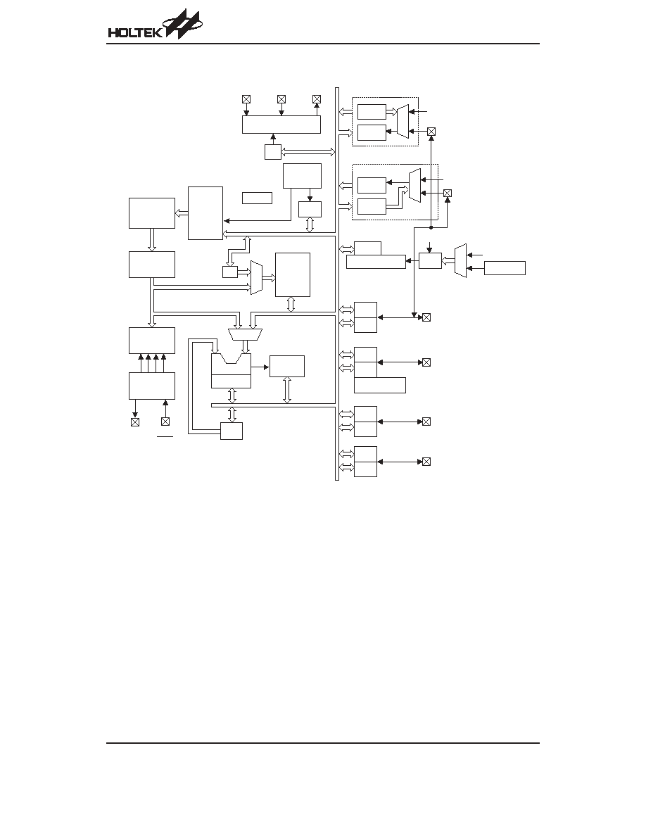
Block Diagram
HT82K96E
Rev. 1.70
2
April 22, 2004
O S C 2
O S C 1
R E S
V D D
M U X
T M R 0 C
T M R 0
V S S
P r o g r a m
R O M
P r o g r a m
C o u n t e r
I n t e r r u p t
C i r c u i t
S T A C K
I N T C
D A T A
M e m o r y
I n s t r u c t i o n
R e g i s t e r
M
U
X
I n s t r u c t i o n
D e c o d e r
S T A T U S
A L U
S h i f t e r
T i m i n g
G e n e r a t o r
A C C
M
U
X
M P
S Y S C L K / 4
W D T S
W D T
W D T O S C
W D T P r e s c a l e r
M
U
X
E N / D I S
P D C
P O R T D
P D 0 ~ P D 7
P B C
P O R T B
P B 0 / A N 0 ~ P B 5 / A N 5
P B 6 / V R L
P B 7 / V R H
P B
P A C
P O R T A
P A 0 ~ P A 5
P A 6 / T M R 0
P A 7 / T M R 1
P A
P D
P C
P O R T C
P C 0 ~ P C 7
P C C
T M R 1 C
T M R 1
M
U
X
P A 7 / T M R 1
f
S Y S
/ 4
f
S Y S
/ 4
P A 6 / T M R 0
A / D C o n v e r t e r
U S B 1 . 1
P S 2
B P
U S B D + / C L K U S B D - / D A T A
V 3 3 O
P A 6
P A 7
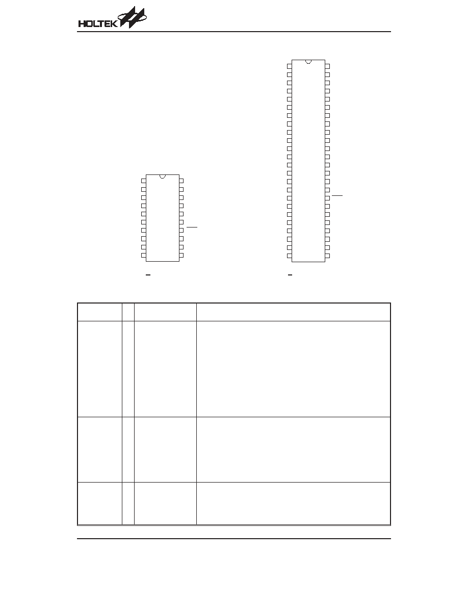
Pin Assignment
Pin Description
Pin Name
I/O
ROM Code
Option
Description
PA0~PA5
PA6/TMR0
PA7/TMR1
I/O
Pull-low
Pull-high
Wake-up
CMOS/NMOS/PMOS
Bidirectional 8-bit input/output port. Each bit can be configured as a
wake-up input by ROM code option. The input or output mode is con-
trolled by PAC (PA control register).
Pull-high resistor options: PA0~PA7
Pull-low resistor options: PA0~PA5
CMOS/NMOS/PMOS options: PA0~PA7
Wake up options: PA0~PA7
PA6 and PA7 are pin-shared with TMR0 and TMR1 input, respectively.
PA0~PA5 can be used as USB mouse X1, X2, Y1, Y2, Z1, Z2 input for
mouse hardware wake-up function
PA6, PA7 can be used as USB mouse button input for mouse hardware
wake-up function
PB0/AN0
PB1/AN1
PB2/AN2
PB3/AN3
PB4/AN4
PB5/AN5
PB6/VRL
PB7/VRH
I/O
Pull-high
Analog input
Bidirectional 8-bit input/output port. Software instructions determine the
CMOS output or Schmitt trigger input with pull-high resistor (determined
by pull-high options).
The PB can be used as analog input of the analog to digital converter
(determined by options).
PB6, PB7 can be used as USB mouse button input for mouse Hardware
wake-up function
PD0~PD7
I/O
Pull-high
Bidirectional I/O lines. Software instructions determine the CMOS out-
put or Schmitt trigger input with pull-high resistor (determined by 1-bit
pull-high option).
PD4 can be used as USB mouse button input for mouse hardware
wake-up function
HT82K96E
Rev. 1.70
3
April 22, 2004
4 8
4 7
4 6
4 5
4 4
4 3
4 2
4 1
4 0
3 9
3 8
3 7
3 6
3 5
3 4
3 3
3 2
3 1
3 0
2 9
2 8
2 7
2 6
2 5
1
2
3
4
5
6
7
8
9
1 0
1 1
1 2
1 3
1 4
1 5
1 6
1 7
1 8
1 9
2 0
2 1
2 2
2 3
2 4
H T 8 2 K 9 6 E
4 8 S S O P - A
P C 6
P C 7
P A 4
P A 5
P A 6 / T M R 0
P A 7 / T M R 1
N C
N C
N C
N C
P D 3
P D 2
P D 1
P D 0
O S C 1
O S C 2
R E S
V S S
P B 7 / V R H
P B 6 / V R L
P B 5 / A N 5
P B 4 / A N 4
P B 3 / A N 3
P B 2 / A N 2
P C 5
P C 4
P A 3
P A 2
P A 1
P A 0
P C 0
P C 1
P C 2
P C 3
N C
N C
N C
N C
P D 4
P D 5
P D 6
P D 7
V D D
V 3 3 O
U S B D + / C L K
U S B D - / D A T A
P B 0 / A N 0
P B 1 / A N 1
2 0
1 9
1 8
1 7
1 6
1 5
1 4
1 3
1 2
1 1
1
2
3
4
5
6
7
8
9
1 0
H T 8 2 K 9 6 E
2 0 S O P - A
P A 3
P A 2
P A 1
P A 0
P C 0
P D 4
V D D
V 3 3 O
U S B D + / C L K
U S B D - / D A T A
P A 4
P A 5
P A 6 / T M R 0
P A 7 / T M R 1
O S C 1
O S C 2
R E S
V S S
P B 7 / V R H
P B 6 / V R L
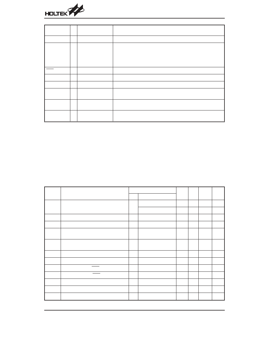
Pin Name
I/O
ROM Code
Option
Description
VSS
¾
¾
Negative power supply, ground
PC0~PC7
I/O
Pull-high
Bidirectional I/O lines. Software instructions determine the CMOS out-
put or Schmitt trigger input with pull-high resistor (determined by
pull-high options).
PC0 can be used as USB mouse IRPT control pin for mouse hardware
wake-up function
RES
I
¾
Schmitt trigger reset input. Active low
VDD
¾
¾
Positive power supply
V33O
O
¾
3.3V regulator output
USBD+/CLK
I/O
¾
USBD+ or PS2 CLK I/O line
USB OR PS2 function is controlled by software control register
USBD-/DATA
I/O
¾
USBD- or PS2 DATA I/O line
USB or PS2 function is controlled by software control register
OSC1
OSC2
I
O
¾
OSC1, OSC2 are connected to an 6MHz or 12MHz Crystal/resonator
(determined by software instructions) for the internal system clock.
Absolute Maximum Ratings
Supply Voltage ...........................V
SS
-0.3V to V
SS
+6.0V
Storage Temperature ............................
-50°C to 125°C
Input Voltage..............................V
SS
-0.3V to V
DD
+0.3V
Operating Temperature...............................0
°C to 70°C
Note: These are stress ratings only. Stresses exceeding the range specified under
²Absolute Maximum Ratings² may
cause substantial damage to the device. Functional operation of this device at other conditions beyond those
listed in the specification is not implied and prolonged exposure to extreme conditions may affect device reliabil-
ity.
D.C. Characteristics
Ta=25
°C
Symbol
Parameter
Test Conditions
Min.
Typ.
Max.
Unit
V
DD
Conditions
V
DD
Operating Voltage
¾
f
SYS
=6MHz
4.4
¾
5.5
V
f
SYS
=12MHz
4.4
¾
5.5
V
I
DD1
Operating Current (6MHz Crystal)
5V
No load, f
SYS
=6MHz
¾
6.5
12
mA
I
DD2
Operating Current (12MHz Crystal)
5V
No load, f
SYS
=12MHz
¾
7.5
16
mA
I
STB1
Standby Current (WDT Enabled)
5V
No load, system HALT,
USB suspend
¾
¾
250
mA
I
STB2
Standby Current (WDT Disabled)
5V
No load, system HALT,
USB suspend
¾
¾
230
mA
V
IL1
Input Low Voltage for I/O Ports
5V
¾
0
¾
0.8
V
V
IH1
Input High Voltage for I/O Ports
5V
¾
2
¾
5
V
V
IL2
Input Low Voltage (RES)
5V
¾
0
¾ 0.4V
DD
V
V
IH2
Input High Voltage (RES)
5V
¾
0.9V
DD
¾
V
DD
V
I
OL1
I/O Port Sink Current for PB, PC1~PC7, PD
5V
V
OL
=3.4V
12
17
¾
mA
I
OL2
I/O Port Sink Current for PB, PC1~PC7, PD
5V
V
OL
=0.4V
2
4
¾
mA
I
OL3
I/O Port Sink Current for PA
5V
V
OL
=0.4V
5
10
¾
mA
HT82K96E
Rev. 1.70
4
April 22, 2004
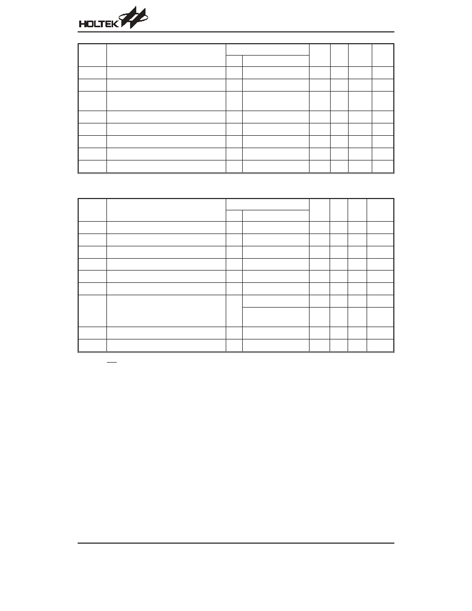
Symbol
Parameter
Test Conditions
Min.
Typ.
Max.
Unit
V
DD
Conditions
I
OL4
I/O Port Sink Current for PC0
5V
V
OL
=0.4V
10
25
¾
mA
I
OH1
I/O Port Source Current for PC0
5V
V
OH
=3.4V
-8
-16
¾
mA
I
OH2
I/O Port Source Current for PA, PB,
PC1~PC7, PD
5V
V
OH
=3.4V
-2
-5
¾
mA
R
PH
Pull-high Resistance for PA, PB, PC, PD
5V
¾
25
50
80
k
W
R
PL
Pull-low Resistance for PA1~PA5
5V
¾
15
30
45
k
W
V
LVR
Low Voltage Reset
¾
¾
3
3.4
4.0
V
V
V33O
3.3V Regulator Output
5V
I
V33O
=
-5mA
3.0
3.3
3.6
V
E
A/D
A/D Conversion Error
5V
Total error
¾
1
2
LSB
A.C. Characteristics
Ta=25
°C
Symbol
Parameter
Test Conditions
Min.
Typ. Max.
Unit
V
DD
Conditions
f
SYS
System Clock (Crystal OSC)
5V
¾
6
¾
12
MHz
f
TIMER
Timer I/P Frequency (TMR0/TMR1)
5V
¾
0
¾
12
MHz
t
WDTOSC
Watchdog Oscillator
5V
¾
15
31
70
ms
t
WDT1
Watchdog Time-out Period (WDT OSC)
5V
Without WDT prescaler
4
8
16
ms
t
WDT2
Watchdog Time-out Period (System Clock)
¾ Without WDT prescaler
¾
1024
¾
t
SYS
t
RES
External Reset Low Pulse Width
¾
¾
1
¾
¾
ms
t
SST
System Start-up Timer Period
¾
Wake-up from HALT
¾
1024
¾
t
SYS
Power-up, Watchdog
Time-out from normal
¾
1024
¾
t
WDTOSC
t
INT
Interrupt Pulse Width
¾
¾
1
¾
¾
ms
t
ADC
A/D Conversion Time
¾
¾
¾
64
¾
t
A/D
Note: t
A/D
=
1
f
A /D
, f
A/D
=A/D clock source frequencies (6MHz, 3MHz, 1.5MHz, 0.75MHz)
HT82K96E
Rev. 1.70
5
April 22, 2004
Document Outline
- þÿ
- þÿ
- þÿ
- þÿ
- þÿ
- þÿ
- þÿ
- þÿ
- þÿ
- þÿ
- þÿ
- þÿ
- þÿ
- þÿ