9_attenuator_smt_section.indd
9
A
T
T
E
N
U
A
T
O
R
S - SM
T
9 - 188
For price, delivery, and to place orders, please contact Hittite Microwave Corporation:
20 Alpha Road, Chelmsford, MA 01824 Phone: 978-250-3343 Fax: 978-250-3373
Order On-line at www.hittite.com
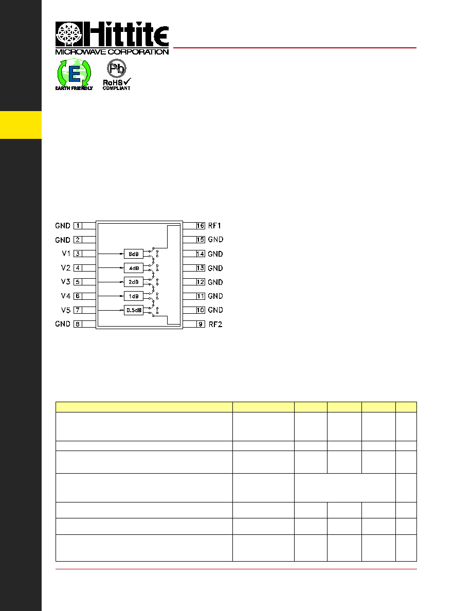
0.5 dB LSB GaAs MMIC 5-BIT DIGITAL
POSITIVE CONTROL ATTENUATOR, 0.7 - 3.8 GHz
General Description
Features
Functional Diagram
The HMC603QS16 & HMC603QS16E are general
purpose broadband 5-bit positive control GaAs IC
digital attenuators in 16 lead QSOP surface mount
plastic packages. Covering 0.7 to 3.8 GHz, the inser-
tion loss is less than 1.9 dB typical. The attenuator
bit values are 0.5 (LSB), 1, 2, 4 and 8 dB for a total
attenuation of 15.5 dB. Attenuation accuracy is excel-
lent at ± 0.15 dB typical with an IIP3 of +50 dBm.
Five bit control voltage inputs, toggled between 0
and +3 to +5V, are used to select each attenuation
state at less than 1 uA each. A single Vdd bias of
+3 to +5V applied through an external 5K Ohm
resistor is required.
0.5 dB LSB Steps to 15.5 dB
Single Positive Control Per Bit
± 0.15 dB Typical Bit Error
High Input IP3: +50 dBm
QSOP16 SMT Package
Electrical Specifications,
T
A
= +25° C, Vdd= +3V to +5V & Vctl= 0/Vdd (Unless Otherwise Stated)
Typical Applications
The HMC603QS16 / HMC603QS16E is ideal for:
· Cellular/3G Infrastructure
· ISM, MMDS
· WLAN, WiMAX, & WiBro
Parameter
Frequency (GHz)
Min.
Typical
Max.
Units
Insertion Loss
0.7 - 1.4 GHz
1.4 - 2.3 GHz
2.3 - 3.0 GHz
3.0 - 3.8 GHz
1.3
1.6
1.9
2.6
1.6
1.9
2.2
3.0
dB
dB
dB
dB
Attenuation Range
15.5
dB
Return Loss (RF1 & RF2, All Atten. States)
0.7 - 1.4 GHz
1.4 - 3.0 GHz
3.0 - 3.8 GHz
18
20
15
dB
dB
dB
Attenuation Accuracy: (Referenced to Insertion Loss)
All States
0.7 -2.2 GHz
2.2 - 3.8 GHz
± (0.2 + 2% of Atten. Setting) Max.
± (0.3 + 3% of Atten. Setting) Max.
dB
dB
Input Power for 0.1 dB Compression
Vdd = 5V
Vdd = 3V
0.7 - 3.8 GHz
29
28
dBm
dBm
Input Third Order Intercept Point
(Two-tone Input Power = 0 dBm Each Tone)
REF - 2 dB States
2.5 - 15.5 dB States
0.7 - 3.8 GHz
53
48
dBm
dBm
Switching Characteristics
0.7 - 3.8 GHz
1.6
1.6
s
s
tRISE, tFALL (10/90% RF)
tON, tOFF (50% CTL to 10/90% RF)
HMC603QS16
/
603QS16E
v00.0805
9
A
T
T
E
N
U
A
T
O
R
S - SM
T
9 - 189
For price, delivery, and to place orders, please contact Hittite Microwave Corporation:
20 Alpha Road, Chelmsford, MA 01824 Phone: 978-250-3343 Fax: 978-250-3373
Order On-line at www.hittite.com
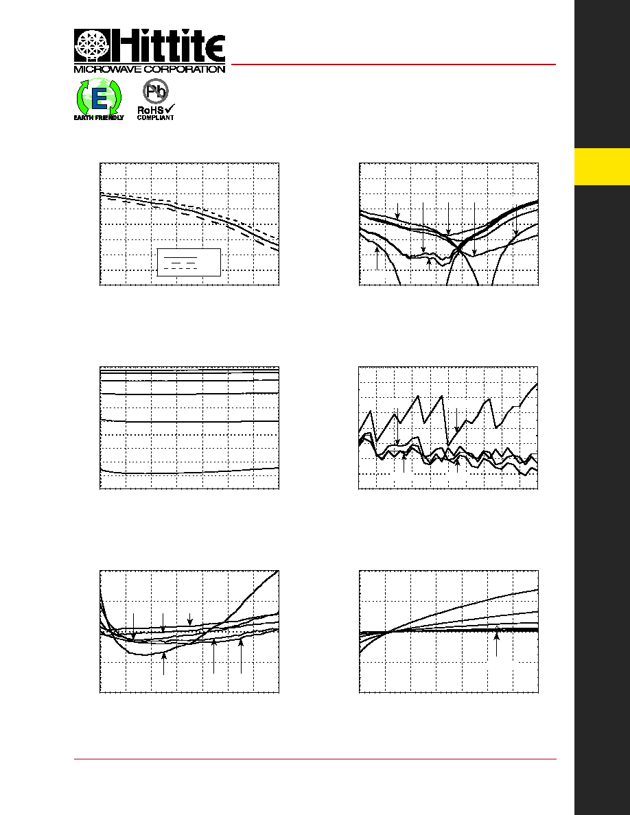
Return Loss RF1, RF2
(Only Major States are Shown)
Bit Error vs. Attenuation State
Insertion Loss
Normalized Attenuation
(Only Major States are Shown)
Bit Error vs. Frequency
(Only Major States are Shown)
Relative Phase vs. Frequency
(Only Major States are Shown)
HMC603QS16
/
603QS16E
v00.0805
-4
-3.5
-3
-2.5
-2
-1.5
-1
-0.5
0
0.5
1
1.5
2
2.5
3
3.5
4
+25 C
+85 C
-40 C
INSERTION LOSS (dB)
FREQUENCY (GHz)
-0.3
-0.2
-0.1
0
0.1
0.2
0.3
0.4
0.5
0.5
2
3.5
5
6.5
8
9.5
11
12.5
14
15.5
BI
T ERROR (dB)
ATTENUATION STATE (dB)
0.9 GHz
1.9 GHz
3.5 GHz
2.4 GHz
-40
-20
0
20
40
0.5
1
1.5
2
2.5
3
3.5
4
RELATIVE PHASE (deg)
FREQUENCY (GHz)
0.5, 1, 2 dB
4 dB
8 dB
15.5 dB
-0.6
-0.3
0
0.3
0.6
0.5
1
1.5
2
2.5
3
3.5
4
BI
T ERROR (dB)
FREQUENCY (GHz)
15.5 dB
8 dB
2 dB
1 dB
4 dB
0.5 dB
-18
-16
-14
-12
-10
-8
-6
-4
-2
0
0.5
1
1.5
2
2.5
3
3.5
4
NORMALIZED ATTENUATION (dB)
FREQUENCY (GHz)
-40
-35
-30
-25
-20
-15
-10
-5
0
0.5
1
1.5
2
2.5
3
3.5
4
RETURN LOSS (dB)
FREQUENCY (GHz)
I.L
0.5 dB
1 dB
2 dB
4 dB
8 dB
15.5 dB
0.5 dB LSB GaAs MMIC 5-BIT DIGITAL
POSITIVE CONTROL ATTENUATOR, 0.7 - 3.8 GHz
9
A
T
T
E
N
U
A
T
O
R
S - SM
T
9 - 190
For price, delivery, and to place orders, please contact Hittite Microwave Corporation:
20 Alpha Road, Chelmsford, MA 01824 Phone: 978-250-3343 Fax: 978-250-3373
Order On-line at www.hittite.com
v00.0805
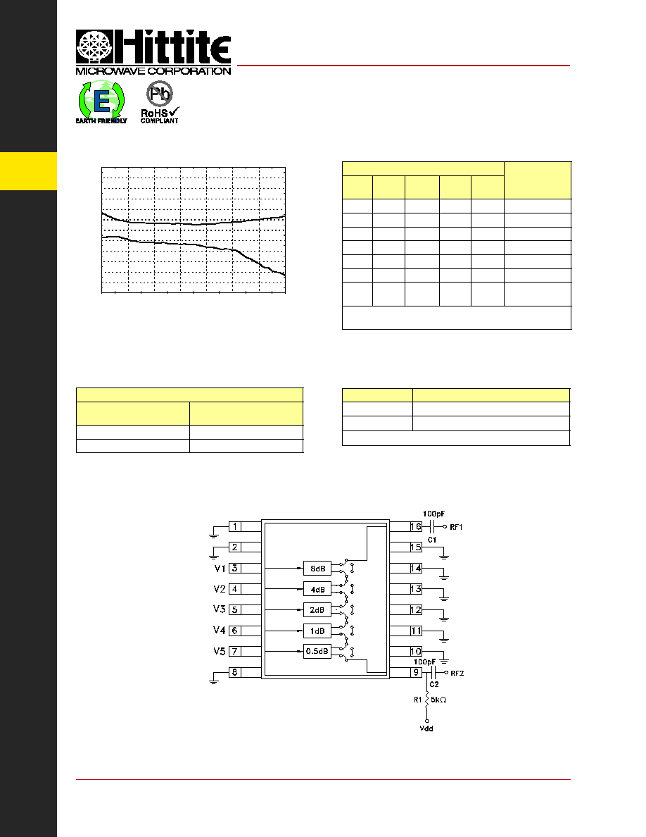
Application Circuit
Note:
DC Blocking Capacitors C1 & C2 are required on RF1 &
RF2. Choose C1 = C2 = 100 ~ 300 pF to allow lowest cus-
tomer specific frequency to pass with minimal loss. R1=
5K Ohm is required to supply voltage to the circuit through
either Pin 9 or Pin 16.
HMC603QS16
/
603QS16E
Truth Table
Control Voltage Input
Attenuation
Setting
RF1 - RF2
V1
8 dB
V2
4 dB
V3
2 dB
V4
1 dB
V5
0.5 dB
High
High
High
High
High
Reference I.L.
High
High
High
High
Low
0.5 dB
High
High
High
Low
High
1 dB
High
High
Low
High
High
2 dB
High
Low
High
High
High
4 dB
Low
High
High
High
High
8 dB
Low
Low
Low
Low
Low
15.5 dB Max.
Atten.
Any combination of the above states will provide an attenuation
approximately equal to the sum of the bits selected.
Worst Case Step Error
-0.6
-0.5
-0.4
-0.3
-0.2
-0.1
0
0.1
0.2
0.3
0.4
0.5
0.6
0.5
1
1.5
2
2.5
3
3.5
4
STEP ERROR (dB)
FREQUENCY (GHz)
Control & Bias Voltages
State
Bias Condition
Low
0 to +0.2V @ 1.0 A Max.
High
Vdd
±
0.2V @ 0.5 A Max.
Note: Vdd = +3V to +5V
±
0.00.20.2
0.2V
Bias Voltage & Current
Vdd = +5.0 Vdc ± 10%
Vdd
(VDC)
Idd (Typ.)
(A)
+3.0
4.0
+5.0
5.0
0.5 dB LSB GaAs MMIC 5-BIT DIGITAL
POSITIVE CONTROL ATTENUATOR, 0.7 - 3.8 GHz
9
A
T
T
E
N
U
A
T
O
R
S - SM
T
9 - 191
For price, delivery, and to place orders, please contact Hittite Microwave Corporation:
20 Alpha Road, Chelmsford, MA 01824 Phone: 978-250-3343 Fax: 978-250-3373
Order On-line at www.hittite.com
v00.0805
Outline Drawing
Absolute Maximum Ratings
RF Input Power (0.7 - 3.8 GHz)
+30 dBm
Control Voltage (V1 - V5)
Vdd + 0.5 Vdc
Bias Voltage (Vdd)
+8.0 Vdc
Channel Temperature
150 °C
Thermal Resistance
174 °C/W
Storage Temperature
-65 to +150 °C
Operating Temperature
-40 to +85 °C
ESD Sensitivity (HBM)
Class 1A
ELECTROSTATIC SENSITIVE DEVICE
OBSERVE HANDLING PRECAUTIONS
NOTES:
1. LEADFRAME MATERIAL: COPPER ALLOY
2. DIMENSIONS ARE IN INCHES [MILLIMETERS].
3. DIMENSION DOES NOT INCLUDE MOLDFLASH OF 0.15mm PER SIDE.
4. DIMENSION DOES NOT INCLUDE MOLDFLASH OF 0.25mm PER SIDE.
5. ALL GROUND LEADS MUST BE SOLDERED TO PCB RF GROUND.
Part Number
Package Body Material
Lead Finish
MSL Rating
Package Marking
[3]
HMC603MS10
Low Stress Injection Molded Plastic
Sn/Pb Solder
MSL1
[1]
HMC603
XXXX
HMC603MS10E
RoHS-compliant Low Stress Injection Molded Plastic
100% matte Sn
MSL1
[2]
HMC603
XXXX
[1] Max peak refl ow temperature of 235 °C
[2] Max peak refl ow temperature of 260 °C
[3] 4-Digit lot number XXXX
Package Information
HMC603QS16
/
603QS16E
0.5 dB LSB GaAs MMIC 5-BIT DIGITAL
POSITIVE CONTROL ATTENUATOR, 0.7 - 3.8 GHz
9
A
T
T
E
N
U
A
T
O
R
S - SM
T
9 - 192
For price, delivery, and to place orders, please contact Hittite Microwave Corporation:
20 Alpha Road, Chelmsford, MA 01824 Phone: 978-250-3343 Fax: 978-250-3373
Order On-line at www.hittite.com
v00.0805
HMC603QS16
/
603QS16E
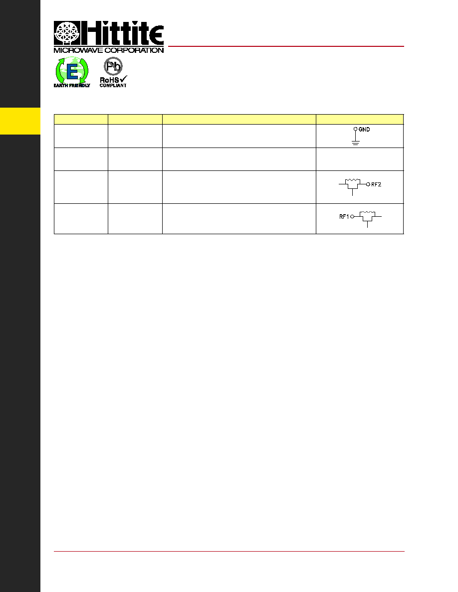
Pin Descriptions
Pin Number
Function
Description
Interface Schematic
1, 2, 8, 10 - 15
GND
These pins must be DC grounded.
3 - 7
V1 - V5
See truth table and control voltage table.
9
RF2
This pin is DC coupled and matched to 50 Ohm.
A blocking capacitor is required.
16
RF1
This pin is DC coupled and matched to 50 Ohm.
A blocking capacitor is required.
0.5 dB LSB GaAs MMIC 5-BIT DIGITAL
POSITIVE CONTROL ATTENUATOR, 0.7 - 3.8 GHz