
DS07-16314-2E
FUJITSU SEMICONDUCTOR
DATA SHEET
32-Bit Microcontroller
CMOS
FR60 MB91307 Series
MB91306R/MB91307R
DESCRIPTION
The FUJITSU FR family of single-chip microcontrollers using a 32-bit high-performance RISC CPU, with a variety
of built-in I/O resources and bus control mechanisms for built-in control applications requiring high-capability,
high-speed CPU processing. External bus access is assumed in order to support the expanded address space
accessible by the 32-bit CPU, and a 1K bytes cache memory plus large RAM are provided for high-speed execution
of CPU instructions.
This microcontroller is ideal for built-in applications such as DVD players, navigation systems, high-capability FAX
and printer control that demand high-capability CPU processing power.
The MB91307 series is a FR60 family product based on the FR30/40 family CPU with enhanced bus access for
higher speed operation.
FEATURES
FR CPU
· 32-bit RISC, load/store architecture, 5-stage pipeline
· Operating frequency 66MHz [with PLL: base frequency 16.5 MHz]
· 16-bit fixed length instructions (basic instructions), 1 instruction per cycle
· Instructions for built-in applications: memory-to-memory transfer, bit processing, barrel shift etc.
· Instructions adapted for high-level languages: function input/output instructions, register contents multi-load/
store instructions
(Continued)
PACKAGE
120-pin, plastic LQFP
(FPT-120P-M21)

MB91307 Series
2
· Easier assembler notation: register interlock function
· Built-in multiplier/instruction level support
Signed 32-bit multiplication: 5 cycles
Signed 16-bit multiplication: 3 cycles
· Interrupt (PC, PS removal): 6 cycles, 16 priority levels
· Harvard architecture for simultaneous execution of program access and data access
· CPU hold 4-word queue allows advanced instruction fetch function
· 4G bytes expanded memory space enables linear access
· Instruction compatible with FR30/40 family
Bus Interface
· Operating frequency: Max 33 MHz
· 8- or 16-bit data output
· Built-in pre-fetch buffer
· Unused data/address pins can be used as general-0purpose input/output ports
· Fully independent 8-area chip select outputs, can be set in minimum 64K bytes units
· Interface support for many memory types
SRAM, ROM/Flash
Page mode flash ROM, page mode ROM interface
Burst mode flash ROM (select burst length 1, 2, 4, 8)
· Basic bus cycle: 2 cycles
· Programmable by area with automatic wait cycle generation to enable wait insert
· RDY input for external wait cycles
· DMA supports fly-by transfer with independent I/O wait control
Built-in RAM
· 128K bytes (MB91307R), 64K bytes (MB91306R)
· Accepts writing of data and instruction codes, enabling use as instruction RAM
Instruction cache
· 1K bytes capacity
· 2-way set associative
· 4-words (16 bytes) per set
· Lock function enables permanent program storage
· Areas not used for instruction cache can be used for RAM
DMAC (DMA controller)
· 5-channel (3-channel external-to-external)
· 3 transfer sources (external pin, internal peripheral, software)
· Addressing mode with 32-bit full address indication (increment, decrement, fixed)
· Transfer mode (demand transfer / burst transfer / step transfer / block transfer)
· Fly-by transfer support (3 channels between external I/O and external memory)
· Transfer data size selection 8/16/32-bit
Bit search module (using REALOS)
· Searches words from MSB for first bit position of a 1/0 change
Reload timer (includes 1 channel for REALOS)
· 16-bit timer: 3 channels
· Internal clock multiplier choice of x2, x8, x32
(Continued)

MB91307 Series
3
(Continued)
UART
· Full duplex double buffer
· 3-channel
· Parity/no parity selection
· Asynchronous (start-stop synchronized), CLK-synchronized communications selection
· Built-in exclusive baud rate timer
· External clock can be used as transfer clock
· Variety of error detection functions (parity, frame, overrun)
I
2
C* interface
Interrupt controller
· Total of 9 external interrupts: 1 non-maskable interrupt pin (NMI) and 8 normal interrupt pins INT7-INT0
· Interrupt from internal peripheral devices
· Programmable priority settings (16 levels) enabled, except for non-maskable interrupt
· Can be used for wake-up from stop mode
A/D converter
· 10-bit resolution, 4-channel
· Sequential comparator type, conversion time approx. 5.4
µ
s
· Conversion modes: single conversion mode, continuous conversion mode
· Startup source: software / external trigger / timer output signal
Other interval timers
· 16-bit timer with 3 channels (U-timer)
· Watchdog timer
I/O port
· Maximum 69 ports
Other features
· Built-in oscillator circuit for clock source, PLL multiplier selection enabled
· INIT reset pin
· Also included: watchdog timer reset, software reset
· Power-saving modes: stop mode, sleep mode supported
· Gear functions
· Built-in time base timer
· Packages: LQFP-120 (FPT-120P-M21) : MB91306R, MB91307R
: MB91V307R (Evaluation products)
· CMOS technology
: 0.25
µ
m : MB91V307R, 0.18
µ
m : MB91306R, MB91307R
· Supply voltage
: MB91V307R : 3.3 V
±
0.3 V (built-in regulator 3.3 V
2.5 V)
: MB91306R, MB91307R : 3.3 V
±
0.3 V, 1.8V
±
0.15 V dual power supplies
* : Purchase of Fujitsu I
2
C components conveys a license under the Philips I
2
C Patent rights to use, these components
in an I
2
C system provided that the system conforms to the I
2
C Standard Specification as defined by Philips.
· Master/slave sending and receiving
· Arbitration function
· Clock synchronization function
· Slave address/general call address detection function
· Transfer direction detection function
· Start condition repeat generator and detection function
· Bus error detection function
· 10-bit/7-bit slave address
· Operates in standard mode (Max 100 Kbps) or high speed mode (Max 400 Kbps)

MB91307 Series
4
PIN ASSIGNMENT
61
62
63
64
65
66
67
68
69
70
71
72
73
74
75
76
77
78
79
80
81
82
83
84
85
86
87
88
89
90
PA3/CS3
PA4/CS4
PA5/CS5
V
CCI
PA6/CS6
PA7/CS7
P80/RDY
P81/BGRNT
P82/BRQ
RD
UUB/WR0
P85/ULB/WR1
NMI
V
CCI
V
SS
INIT
P90/SYSCLK
P91
P92/MCLK
P93
P94/LBA/AS
P95/BAA
P96
P97/WE
P20/D16
P21/D17
P22/D18
P23/D19
P24/D20
P25/D21
PI5/SC1
PI4/SO1
PI3/SI1
PI2/SC0
PI1/SO0
PI0/SI0
V
CC
PJ7/INT7/ATG
PJ6/INT6/TIN2
PJ5/INT5/TIN1
PJ4/INT4/TIN0
PJ3/INT3
PJ2/INT2
PJ1/INT1
PJ0/INT0
AN3
AN2
AN1
AN0
AV
SS
/AVRL
AVRH
AV
CC
A24/P70
A23/P67
A22/P66
A21/P65
A20/P64
A19/P63
A18/P62
A17/P61
30
29
28
27
26
25
24
23
22
21
20
19
18
17
16
15
14
13
12
11
10
9
8
7
6
5
4
3
2
1
91
92
93
94
95
96
97
98
99
100
101
102
103
104
105
106
107
108
109
110
111
112
113
114
115
116
117
118
119
120
P26/D22
P27/D23
D24
D25
D26
D27
D28
D29
D30
D31
V
SS
A00
A01
A02
A03
A04
A05
A06
A07
V
CC
A08
A09
A10
A11
A12
A13
A14
A15
V
SS
P60/A16
P
A2/CS2
P
A1/CS1
P
A0/CS0
PB7/IORD
PB6/IO
WR
V
CC
X0
X1
V
SS
PB5/DEOP1/DSTP
1
PB4/D
A
CK1
PB3/DREQ1
PB2/DEOP0/DSTP
0
PB1/D
A
CK0
PB0/DREQ0
MD2
MD1
MD0
PG2/DEOP2/DSTP
2
PG1/D
A
CK2
PG0/DREQ2
PH7/SCL
PH6/SD
A
PH5/T
O
T
2
PH4/T
O
T
1
PH3/T
O
T
0
V
SS
PH2/SC2
PH1/SO2
PH0/SI2
60
59
58
57
56
55
54
53
52
51
50
49
48
47
46
45
44
43
42
41
40
39
38
37
36
35
34
33
32
31
* : "L" level output after initialization and reset
FPT-120P-M21

MB91307 Series
5
PIN DESCRIPTIONS
(Continued)
Pin no.
Pin name
I/O
circuit type
Description
85 to 92
D16 to D23
C
External data bus bit 16 to bit 23
Valid only in external bus 16-bit mode.
P20 to P27
These pins can be used as ports in external bus 8-bit mode
93 to 100
D24 to D31
C
External data bus bit 24 to bit 31
102 to 109
A00 to A07
F
External address output bit0 to bit7
111 to 118
A08 to A15
F
External address output bit8 to bit15
120, 1 to 7
A16 to A23
F
External address output bit16 to bit23
P60 to P67
These pins can be used as ports according to setting
8
A24
F
External data bus output bit24
P70
This pin can be used as a port according to setting
9
AV
CC
Power supply pin. Analog power supply for A/D converter
10
AVRH
A/D converter reference voltage supply
11
AV
SS
/AVRL
Power supply pin. Analog power supply for A/D converter
12 to 15
AN0 to AN3
D
A/D converter reference voltage supply. Analog input pin.
16 to 19
INT0 to INT3
I
External interrupt input. When the corresponding external interrupt is en-
abled, this input is in use at all times, so that output from other functions
must be stopped unless used intentionally
PJ0 to PJ3
General purpose input/output port
20 to 22
TIN0 to TIN2
I
Reload timer input. When the corresponding timer input is enabled, this
input is in use at all times, so that output from other functions must be
stopped unless used intentionally.
INT4 to INT6
External interrupt input. When the corresponding external interrupt is en-
abled, this input is in use at all times, so that output from other functions
must be stopped unless used intentionally.
PJ4 to PJ6
General purpose input/output port
23
ATG
I
A/D converter external trigger input. When selected as an A/D start
source, this input is in use at all times, so that output from other functions
must be stopped unless used intentionally.
INT7
External interrupt input. When the corresponding external interrupt is en-
abled, this input is in use at all times, so that output from other functions
must be stopped unless used intentionally.
PJ7
General purpose input/output port
25
SI0
F
UART0 data input. When the UART0 channel is in input operation, this
input is in use at all times, so that output from other functions must be
stopped unless used intentionally.
PI0
General purpose input/output port.
26
SO0
F
UART0 data output. This function is valid when the UART0 data output
function setting is disabled.
PI1
General purpose input/output port. This function is valid when the
UART0 data output function setting is disabled.

MB91307 Series
6
(Continued)
Pin no.
Pin name
I/O
circuit type
Description
27
SC0
F
UART0 clock output. The clock output is valid when the UART0 clock
output function setting is enabled.
PI2
General purpose input/output port. This function is valid when the
UART0 clock output function is disabled.
28
SI1
F
UART1 data input. When UART1 is set for input operation, this input is
in use at all times, so that output from other functions must be stopped
unless used intentionally.
PI3
General purpose input/output port.
29
SO1
F
UART1 data output. This function is enabled when the UART1 data out-
put function setting is enabled.
PI4
General purpose input/output port. This function is valid when the
UART1 data output function setting is disabled.
30
SC1
F
UART1 clock input/output. The clock output is enabled when the UART1
clock output function setting is enabled.
PI5
General purpose input/output port. This function is valid when the
UART1 clock output function setting is disabled.
31
SI2
F
UART2 data input. When UART2 is set for input operation, this input is
in use at all times, so that output from other functions must be stopped
unless used intentionally.
PH0
General purpose input/output port.
32
SO2
F
UART2 data output. This function is enabled when the UART2 data out-
put function setting is enabled.
PH1
General purpose input/output port This function is enabled when the
UART2 data output function setting is disabled.
33
SC2
F
UART2 clock input/output. The clock output is enabled when the UART2
clock output function setting is enabled.
PH2
General purpose input/output port This function is enabled when the
UART2 clock output function is disabled.
35
TOT0
C
Timer output port. This function is valid when the timer output setting is
enabled.
PH3
General purpose input/output port.This pin outputs an "L" level signal at
reset.
36
TOT1
C
Timer output port. This function is valid when the timer output setting is
enabled.
PH4
General purpose input/output port.This pin outputs an "L" level signal at
reset.
37
TOT2
C
Timer output port. This function is valid when the timer output is enabled.
PH5
General purpose input/output port.

MB91307 Series
7
(Continued)
Pin no.
Pin name
I/O
circuit type
Description
38
SDA
Q
I
2
C bus input/output port. This function is valid when I
2
C operation is en-
abled. When the I
2
C bus is in use, the port output must be set to Hi-Z
level. When the I
2
C bus is in use, this is an open drain pin.
PH6
General purpose input/output port.
39
SCL
Q
I
2
C bus input/output port. This function is valid when I
2
C operation is en-
abled. When the I
2
C bus is in use, the port output must be set to Hi-Z
level. When the I
2
C bus is in use, this is an open drain pin.
PH7
General purpose input/output port.
40
DREQ2
F
DMA external transfer request input. When selected as a DMA startup
source, this input is in use at all times, so that output from other functions
must be stopped unless used intentionally.
PG0
General purpose input/output port.
41
DACK2
F
DMA external transfer request acknowledge output. This function is valid
when the DMA transfer request acknowledge output setting is enabled.
PG1
General purpose input/output port. This function is valid when the DMA
transfer request acknowledge output setting is enabled.
42
DEOP2
F
DMA external transfer end output. This function is valid when the DMA
external transfer end output setting is enabled.
DSTP2
DMA external transfer stop input. This function is valid when the DMA ex-
ternal transfer stop input setting is enabled.
PG2
General purpose input/output port. This function is valid when the DMA
external transfer end output selection and the DMA external transfer stop
input selection are disabled.
43 to 45
MD2 to MD0
G
Mode pins 2 to 0. The setting of these two pins determines the basic
operating mode. They should be connected to V
cc
or V
ss
.
46
DREQ0
F
DMA external transfer request input. When selected as a DMA startup
source, this input is in use at all times, so that output from other functions
must be stopped unless used intentionally.
PB0
General purpose input/output port.
47
DACK0
F
DMA external transfer request acknowledge output. This function is valid
when the DMA transfer request acknowledge output setting is enabled.
PB1
General purpose input/output port. This function is enabled when the
DMA transfer request acknowledge output setting is disabled.
48
DEOP0
F
DMA external transfer end output. This function is valid when the DMA
external transfer end output setting is enabled.
DSTP0
DMA external transfer stop input. This function is valid when the DMA ex-
ternal transfer stop input setting is enabled.
PB2
General purpose input/output port. This function is valid when the DMA
external transfer end output selection and the DMA external transfer stop
input selection are disabled.

MB91307 Series
8
(Continued)
Pin no.
Pin name
I/O
circuit type
Description
49
DREQ1
F
DMA external transfer request input. When selected as a DMA startup
source, this input is in use at all times, so that output from other functions
must be stopped unless used intentionally.
PB3
General purpose input/output port.
50
DACK1
F
DMA external transfer request acknowledge output. This function is valid
when the DMA transfer request acknowledge output setting is enabled.
PB4
General purpose input/output port. This function is enabled when the
DNA transfer request acknowledge output setting is disabled.
51
DEOP1
F
DMA external transfer end output. This function is valid when the DMA
external transfer end output setting is enabled.
DSTP1
DMA external transfer stop input. This function is valid when the DMA ex-
ternal transfer stop input setting is enabled.
PB5
General purpose input/output port. This function is valid when the DMA
external transfer end output selection and the DMA external transfer stop
input selection are disabled.
53
X1
A
Clock (oscillator) output
54
X0
Clock (oscillator) input
56
IOWR
F
Write strobe output for DMA fly-by transfer. This function is valid when
the DMA fly-by transfer write strobe output setting is enabled.
PB6
General purpose input/output port. This function is valid when the DMA
fly-by transfer write strobe output setting is disabled.
57
IORD
F
Read strobe output for DMA fly-by transfer. This function is valid when
the DMA fly-by transfer read strobe output setting is enabled.
PB7
General purpose input/output port. This function is valid when the DMA
fly-by transfer read strobe output setting is disabled.
58
CS0
F
Chip select output. This function is valid when the chip select 0 output
setting is enabled.
PA1
General purpose input/output port. This function is valid when the chip
select 0 output setting is disabled.
59
CS1
F
Chip select output. This function is valid when the chip select 1 output
setting is enabled.
PA1
General purpose input/output port. This function is valid when the chip
select 1 output setting is disabled.
60
CS2
F
Chip select output. This function is valid when the chip select 2 output
setting is enabled.
PA2
General purpose input/output port. This function is valid when the chip
select 2 output setting is disabled.
61
CS3
F
Chip select output. This function is valid when the chip select 3 output
setting is enabled.
PA3
General purpose input/output port. This function is valid when the chip
select 3 output setting is disabled.

MB91307 Series
9
(Continued)
Pin no.
Pin name
I/O
circuit type
Description
62
CS4
F
Chip select output. This function is valid when the chip select 4 output set-
ting is enabled.
PA4
General purpose input/output port. This function is valid when the chip se-
lect 4 output setting is disabled.
63
CS5
F
Chip select output. This function is valid when the chip select 5 output set-
ting is enabled.
PA5
General purpose input/output port. This function is valid when the chip se-
lect 5 output setting is disabled.
64
V
CCI
Internal Power supply pin (1.8 V power supply) .
65
CS6
F
Chip select output. This function is valid when the chip select 6 output set-
ting is enabled.
PA6
General purpose input/output port. This function is valid when the chip
select 6 output setting is disabled.
66
CS7
F
Chip select output. This function is valid when the chip select 7 output set-
ting is enabled.
PA7
General purpose input/output port. This function is valid when the chip
select 7 output setting is disabled.
67
RDY
C
External ready signal input. This function is valid when the external ready
input setting is enabled.
P80
General purpose input/output port. This function is valid when the exter-
nal ready input setting is disabled.
68
BGRNT
F
External bus open acknowledge output. This pin outputs an L level signal
when the external bus is open. This function is valid when the output set-
ting is enabled.
P81
General purpose input/output port. This function is valid when the output
setting is disabled.
69
BRQ
P
External bus open request input. The input value is "1" when the external
bus is open. This function is valid when the input setting is enabled.
P82
General purpose input/output port. This function is valid when the input
setting is disabled.
70
RD
M
External bus read strobe output.
71
WR0
UUB
F
External bus write strobe output.
Upper side of the 16-bit SRAM input/output mask enable signal.
It is valid when the external bus is set to SRAM use. (WE/P97 function as
the write strobe.)
72
WR1
ULB
F
External bus write strobe output.
Lower side of the 16-bit SRAM input/output mask enable signal.
It is valid when the external bus is set to SRAM use. (WE/P97 function as
the write strobe.)
P85
General purpose input/output port. This function is valid when the enable
output setting is disabled.

MB91307 Series
10
(Continued)
Pin no.
Pin name
I/O
circuit type
Description
73
NMI
H
NMI
request
input
74
V
CCI
H
Internal Power supply pin(1.8 V power supply)
76
INIT
B
External reset input
77
SYSCLK
F
System clock output. This function is valid when the system clock output
setting is enabled. The clock signal output is at the same frequency as the
external bus operating frequency. Clock output halts in the stop mode or
the hardware standby mode.
P90
General purpose input/output port. This function is enabled when the sys-
tem clock output setting is disabled.
78
P91
F
General purpose input/output port. This function is enabled when the
SDRAM clock enable output setting is disabled.
79
MCLK
F
Memory clock output. Clock output halts in the sleep mode, the stop mode
or the hardware standby mode.
P92
General purpose input/output port. This function is enabled when the
clock output setting is disabled.
80
P93
F
General purpose input/output port. This function is enabled when the
SDRAM clock re-input setting is disabled.
81
AS
F
Address strobe output. This function is valid when the address strobe out-
put setting is disabled.
LBA
Burst flash ROM address load output. This function is valid when the ad-
dress load output setting is enabled.
P94
General purpose input/output port. This function is valid when the address
load output and address strobe output settings are disabled.
82
BAA
Burst flash ROM address advance output. This function is valid when the
address advance output setting is enabled.
P95
General purpose input/output port. This function is valid when the address
advance output and column address strobe output settings are disabled.
83
P96
F
General purpose input/output port. This function is enabled when the col-
umn address strobe output setting is disabled.
84
WE
Write strobe output for 16-bit SRAM. This function is enabled when the
write strobe output setting is enabled.
P97
General purpose input/output port. This function is enabled when the write
strobe output setting is prohibited.
9
AV
CC
A/D converter power supply
10
AVRH
A/D converter power supply
11
AV
SS
/AVRL
A/D converter power supply (GND)
24, 55,
110
V
CC
Power supply pins
34, 52,
75, 101
V
SS
Power supply pins (GND)

MB91307 Series
11
I/O CIRCUIT TYPE
(Continued)
Type
Circuit
Remarks
A
· Oscillator feedback resistance
approx. 1 M
B
· CMOS hysteresis input
with pull-up resistance (25 k
)
C
· CMOS level input/output
with standby control
D
· Analog input with switch
X1
STANDBY
CONTROL
X0
clock input
digital input
STANDBY CONTROL
digital input
digital output
digital output
CONTROL
analog input

MB91307 Series
12
(Continued)
Type
Circuit
Remarks
F
· CMOS level output
· CMOS level hysteresis input
with standby control
G
· CMOS level input
without standby control
H
· CMOS level hysteresis input
without standby control
I
· CMOS level input
· CMOS level hysteresis input
without standby control
M
· CMOS level input
STANDBY CONTROL
digital output
digital input
digital output
digital input
digital input
digital output
digital input
digital output
digital output
digital output

MB91307 Series
13
(Continued)
Type
Circuit
Remarks
P
· CMOS level input/output
with standby control
with pull-down resistance (25 k
)
Q
· Open drain output
CMOS level hysteresis input
with standby control
STANDBY CONTROL
CONTROL
digital output
digital input
digital output
STANDBY CONTROL
digital input
Open drain control
digital output

MB91307 Series
14
HANDLING DEVICES
MB91307 Series
·
Preventing Latchup
When CMOS integrated circuit devices are subjected to applied voltages higher than V
CC
at input and output
pins (other than medium- and high-withstand voltage pins), or to voltages lower than V
SS
, as well as when voltages
in excess of rated levels are applied between V
CC
and V
SS
, a phenomenon known as latchup can occur. When
a latchup condition occurs, supply current can increase dramatically and may destroy semiconductor elements.
In using semiconductor devices, always take sufficient care to avoid exceeding maximum ratings.
·
Treatment of unused pins
Do not leave an unused input pin open, since it may cause a malfunction. Handle by, using a pull-up or
pull-down resistor.
·
About power supply pins
In products with multiple V
CC
or V
SS
pins, the pins of the same potential are internally connected in the device
to avoid abnormal operations including latch-up. However, you must connect the pins to external power supply
and a ground line to lower the electro-magnetic emission level, to prevent abnormal operation of strobe signals
caused by the rise in the ground level, and to conform to the total output current rating.
Moreover, connect the current supply source with the V
CC
and V
SS
pins of this device at the low impedance.
It is also advisable to connect a ceramic bypass capacitor of approximately 0.1 mF between V
CC
and V
SS
near
this device.
·
Notes on Power-ON/shut-down
Cautions to take when turning on/off V
CCI
(1.8-V internal power supply) and V
SS
(3.3-V external-pin power
supply)
Do not apply V
SS
(external) alone continuously (for over an indication of one minute) with V
CCI
(internal) discon-
nected not to cause a reliability problem with the LSI.
When V
SS
(external) returns from the OFF state to the ON state, the circuit may fail to hold its internal state, for
example, due to power supply noise.
·
Precautions for use of stop mode
The built-in regulator in this device stops operating when the device is in stop mode. In such cases as when
increased leak current (I
CCH
) in stop mode, or abnormal operation or power fluctuation due to noise while in
operating mode cause the regulator to stop, the internal 2.5 V power supply can ball below the voltage at which
operation is assured. Therefore it is necessary when using the internal regulator and stop mode to assure that
the external power supply does not fall below 3.3 V. And even if this should occur, the internal regulator can be
set to restart when a reset is applied. (In this case the oscillator stabilization wait period should also be set to
"L" level.)
When the power is turned on
V
CCI
(internal)
V
SS
(external)
Signal
When the power is turned off
Signal
V
SS
(external)
V
CCI
(internal)

MB91307 Series
15
· Sample use of Stop Mode with 3.3 V power supply
·
About crystal oscillator circuit
Noise near the X0 and X1 pins may cause the device to malfunction. Design the printed circuit board so that
X0, X1, the crystal oscillator (or ceramic oscillator) , and the bypass capacitor to ground are located as close to
the device as possible.
It is strongly recommended to design the PC board artwork with the X0 and X1 pins surrounded by ground plane
because stable operation can be expected with such a layout.
·
Treatment of NC pins
Any pins marked "NC" (not connected) must be left open.
·
About mode pins (MD0 to MD2)
Mode pins (MD0 to MD2) should be connected directly to V
CC
or V
SS
.
To prevent the device erroneously switching to test mode due to noise, design the printed circuit board such that
the distance between the mode pins and V
CC
or V
SS
is as short as possible and the connection impedance is low.
·
Operation at startup
Immediately after a power-on startup, always apply a reset initialization (INIT) at the INIT pin. Also, in order to
assure a wait period for the oscillator circuits to stabilize immediately after startup, be sure that the "L" level input
to the INIT pin continues for the required stabilization wait interval. (The INIT cycle for the INIT pin includes only
the minimum setting for the stabilization wait period.)
·
Base oscillator input at startup
At power-on startup, always input a clock signal until the oscillator stabilization wait period is ended.
·
Caution on Operations during PLL Clock Mode
If the PLL clock mode is selected, the microcontroller attempt to be working with the self-oscillating circuit even
when there is no external oscillator or external clock input is stopped. Performance of this operation, however,
cannot be guaranteed.
·
Precaution on using ports 6 and 7
If one of P60/A15 to P70/A24, which are shared for output of external bus interface addresses, is used as a port,
a grid voltage is applied to the port instantaneously when the status of another address output pin is changed.
Therefore, add resistors or capacitors to those ports to prevent application of the grid voltage.
V
CC
C
V
SS
0.1 F
3.3 V
2.4 k
7.6 k
GND

MB91307 Series
16
·
Clock control block
For L-level input to the INIT pin, allow for the regulator settling time or oscillation settling time.
·
Bit search module
The 0-detection, 1-detection, and transition-detection data registers (BSD0, BSD1, and BSDC) are only word-
accessible.
·
Prefetch
When accessing a prefetch-enabled little endian area, use word access only (access in 32 bits).
Byte or halfword access results in wrong data read.
·
Setting of external bus
The MB91307 series is guaranteed at an external bus frequency of 33 MHz. As the external bus is capable of
supporting 66 MHz for future enhancements, the initial value is the same rate as the base clock (determined by
the PLL setting) . The external bus is set to 66 MHz if you set the base clock to 66 MHz with the external-bus
base clock division setting register (DIVR1) containing the initial value. To change the base clock frequency, set
the external bus frequency not exceeding 33 MHz and set the new base clock frequency.
·
MCLK and SYSCLK
MCLK causes a stop in SLEEP/STOP mode while SYSCLK causes a stop only in STOP mode. Use either
depending on each application.
·
I
2
C input/output pin
The SDA and SCL pins of the MB91307 series are pseudo open-drain pins with the P-ch transistor turned off
to prevent the "H" level from being output. As the circuit configuration has a diode added to the V
CC
side, therefore,
the communication voltage must be adjusted to the 3.3-V power supply of this model (pulled up to a voltage of
3.3 V) .
·
Shared port function switching
To switch a pin that also serves as a port, use the port function register (PFR). Note, however, that bus pins are
switched depending on external bus settings.
·
Pull-up control
Connecting a pull-up resistor to the pin serving as an external bus pin cannot a guarantee the AC standard.
Even the port for which a pull-up resistor has been set is invalid in stop mode with HIZ = 1 or in hardware standby
mode.
·
I/O port access
Byte access only for access to port
·
Remarks for the external clock operation
When selecting the external clock, active X0 pin generally. Also simultaneously the opposite phase clock to X0
must be supplied to X1 pin. When using the clock along with STOP (oscillation stopped) mode, the X1 pin stops
when "H" is input in STOP mode. To prevent one output from competing against another, in this case, the stop
mode must not be used.

MB91307 Series
17
·
Low-power consumption modes
·
To enter the standby mode, use the synchronous standby mode (set with the SYNCS bit as bit 8 in the
TBCR, or time-base counter control register) and be sure to use the following sequence:
(LDI
#value_of_standby, R0)
(LDI
#_STCR, R12)
STB
R0, @R12
; Write to standby control register (STCR)
LDUB
@R12, R0
; Read STCR for synchronous standby
LDUB
@R12, R0
; Read STCR again for dummy read
NOP
; NOP x 5 for timing adjustment
NOP
NOP
NOP
NOP
Set the I-flag and the ILM and ICR registers to branch to an interrupt handler when the interrupt handler
triggers the microcontroller to return from the standby mode.
·
If you use the monitor debugger, follow the precautions below:
Do not set a breakpoint within the above array of instructions.
Do not single-step the above array of instructions.
·
Current at power-on (only for MB91V307R)
About 300 mA of power supply current flows when the power is turned on with INIT set to 0.
Set INIT to 1 to stop the overcurrent flowing. After that, the overcurrent will not flow even if INIT is set to 0.
·
Watchdog timer
The watchdog timer function of this model monitors that a program delays a reset within a certain period of time
and resets the CPU if the program fails to delay it, for example, because the program runs out of control. Once
the watchdog timer function is enabled, therefore, the watchdog timer countinues to operate until a reset takes
place.
An exception, for example during stop, sleep and DMA transfer modes, is the automatic delaying of a reset under
a condition in which the CPU stops program execution.
Note, however, that a watchdog reset may not occur in the above state caused when the system runs out of
control. If this is the case, use the external INIT pin to cause a reset (INIT).
MB91307 series
X0
X1
Using external clock (normal)
Note : Stop mode (oscillation stop mode) cannot be used.

MB91307 Series
18
·
Terminal and timing control register (TCR) (0x00000683)
The terminal and timing control register (TCR) is a write-only register. Therefore, do not access TCR with a bit
manipulation instruction.
If you intend to disable sharing of the bus by writing "0" to Bit 7 (BREN bit) of TCR when the bit is "1", be sure
to follow the procedure below. If the procedure is not followed, the device may hang up.
1. Write "0" to Bit 2 (BRQE bit) of the port 8 function register (PFR8).
2. Write "0" to Bit 7 (BREN bit) of TCR.
·
RD/WR
CS hold extension cycle
Assume that use of the RD/WR
CS hold extension cycle is specified (Bit 0 of AWR is 1) for an
area for which the normal memory/IO access type is set (the TYPE3 to TYPE0 bits of ACR are
0xxx). Even in this case, the hold extension cycle might not be inserted when the operation and
settings are specified in a specific combination.
The hold extension cycle will not be inserted when the following conditions are met:
· Use of the RD/WR
CS hold extension cycle is specified.
(Bit 0 [W00 bit] of AWR is 1.)
· A normal memory/IO access type is set for the area.
(Bits 3 to 0 [TYPE3 to TYPE0 bits] of ACR are 0xxx.)
Note: The MB91307 series allows only this type to be set.
· Disuse of the address
CS delay cycle is specified.
(Bit 2 [W02 bit] of AWR is 0.)
· A setting (recovery enabled) other than 0 cycle is made for the write recovery cycle.
(Bits 5 and 4 [W05 and W04 bits] of AWR are other than 00.)
(Example: First word writing to an external bus 16-bit area)
· If an access is made to write data larger than the bus width to the relevant area under the above conditions,
the RD/WR-CS hold extension cycle is not inserted in any cycle other than the last cycle to write divisions of
the data. Therefore, the hold time becomes insufficient.
Note : This problem does not occur in the read cycle.
To use this function, make either of the following settings:
· Specify the use of the address
CS delay cycle.
(Set 1 for Bit 2 [W02 bit] of AWR.)
· Specify 0 cycle for the write recovery cycle.
(Set 00 for Bits 5 and 4 [W05 and W04 bits] of AWR.)
·
Signed DIVIDE statement (DIVOS)
When the instruction immediately before the instruction of DIVOS is an instruction by which the memory access
is done, a correct calculation result might not be obtained.
This is generated under the following conditions.
· When the instruction performs memory accesses just before a DIVOS instruction.
Note : Instructions that performs relevant memory accesses (a total of 58 instructions)
ST Ri, @- R15
ST Rs, @- R15
ST PS, @- R15
STB Ri, @Rj
STB Ri, @ (R13, Rj)
DMOVB R13, @dir8
STB Ri, @ (R14, disp8)
LDUB @Rj, Ri
LD @ (R13, Rj), Ri
LDUH @ (R13, Rj), Ri
LDUB @ (R13, Rj), Ri
DMOV @dir10, R13
DMOVH @dir9, R13
DMOVB @dir8, R13
LD @ (R14, disp10), Ri

MB91307 Series
19
LDUH @ (R14, disp9), Ri
LDUB @ (R14, disp8), Ri
AND Rj, @Ri
ANDH Rj, @Ri
ANDB Rj, @Ri
ORB Rj, @Ri
EORB Rj, @Ri
DMOV @R13+, @dir10
DMOVH @R13+, @dir9
DMOVB @R13+, @dir8
DMOV @dir10, @R13+
DMOVH @dir9, @R13+
DMOVB @dir8, @R13+
DMOV @R15+, @dir10
DMOV @dir10, @- R15
· When full trace mode is specified as trace mode and the DIVOS and DIV1 instructions are not 4-byte aligned.
· Even if the DIVOS and DIV1 instructions are 4-byte aligned, perform a D-bus DMA transfer or specify the full
trace mode as trace mode if a breakpoint is set in the DIV1 instruction.
Avoid this notes as follows:
(1) Do not place an instruction that performs memory access before a DIVOS instruction.
(2) Do not perform a DMA transfer to the D-bus or set full trace mode as trace made when a DIVOS instruction
is specified.
To output the code for avoiding above (1) condition, specify "-@div0s 1" as the compiler option.
SOFTUNE compiler:
· In case of using the SOFTUNE V3: after the SOFTUNE compiler V30L07R07
· In case of using the SOFTUNE V5: after the SOFTUNE compiler V50L04
· In case of using the SOFTUNE V6: after the SOFTUNE compiler V60L01
·
DMA demand transfer
In sleep mode, demand transfer is executed only once and processing does not go further. During normal
operation, the efficiency of demand transfers may seem to be lowered.
This action occurs only in demand transfers (it does not occur in DREQ edge detection mode or the like).
This is occurred in the following cases:
· A demand transfer by DMAC is performed in sleep mode.
- After a demand transfer is performed once, processing does not go further although DREQ is input
successively.
- A subsequent transfer is started if the device is released from sleep mode and an external bus operation
other than a DMA transfer occurs.
· A demand transfer by DMAC is performed during normal operation.
- After a demand transfer is performed once, a subsequent transfer is not performed until an external bus
access other than a DMA transfer occurs.
- A demand transfer does not progress while there is no external bus access because cache hitting is
performed continuously or internal ROM operation continues.
· A subsequent demand transfer is not started even if an external bus access for prefetching occurs.
Avoid this notes as follows:
· Do not perform a demand transfer by DMAC in sleep mode.
· Do not use sleep mode during a demand transfer by DMAC.

MB91307 Series
20
·
RMW instructions using R15
If one of the instructions listed below is executed, the value of SSP or USP* is not used as the value of R15 and,
as a result, an incorrect value is written to memory. Therefore, the compiler does not generate the following
instructions:
AND
R15,@Rj ANDH
R15,@Rj ANDB
R15,@Rj
OR
R15,@Rj ORH
R15,@Rj ORB
R15,@Rj
EOR
R15,@Rj EORH
R15,@Rj EORB
R15,@Rj
XCHB
@Rj,R15
* : R15 is an insubstantial register. If R15 is accessed by a program, SSP or USP is accessed according to the
state of the S flag of the PS register.
Avoid this notes as follows:
· When programming any of the above 10 instructions by an assembler, specify a general-purpose register in
place of R15.
·
Executing instructions on RAM
· If instruction codes are placed in RAM, they should not be placed in the last 8 address bytes 0005 FFF8
H
to
0005 FFFF
H
. (Instruction code prohibited area)
·
Notes on the PS register
Since some instructions manipulate the PS register earlier, the following exceptions may cause the interrupt
handler to break or the PS flag to update its display setting when the debugger is being used. As the microcon-
troller is designed to carry out reprocessing correctly upon returning from such an EIT event, it performs oper-
ations before and after the EIT as specified in either case.
·
The following operations may be performed when the instruction immediately followed by a DIVOU/DIVOS
instruction is (a) halted by a user interrupt or NMI, (b) single-stepped, or (c) breaks in response to a data
event or emulator menu:
(1) D0 and D1 flags are updated earlier.
(2) The EIT handler (user interrupt/NMI or emulator) is executed.
(3) Upon returning from the EIT, the DIVOU/DIVOS instruction is executed and the D0 and D1 flags are
updated to the same values as those in (1) above.
·
The following operations are performed when the ORCCR/STILM/MOV Ri and PS instructions are executed
to enable interruptions when a user interrupt or NMI trigger event has occurred.
(1) The PS register is updated earlier.
(2) The EIT handler (user interrupt/NMI or emulator) is executed.
(3) Upon returning from the EIT, the above instructions are executed and the PS register is updated to the
same value as that in (1) above.
·
Notes on I-bus Memory
Do not access data in the instruction cache control register or the instruction cache RAM immediately before
the RETI instruction.

MB91307 Series
21
Unique to the evaluation chip MB91V307R
·
Simultaneous occurrences of a software break and a user interrupt/NMI
When a software break and a user interrupt /NMI take place at the same time, the emulator debugger can cause
the following phenomena:
·
The debugger stops pointing to a location other than the programmed breakpoints.
·
The halted program is not re-executed correctly.
If these phenomena occur, use a hardware break instead of the software break. If the monitor debugger has
been used, avoid setting any break at the relevant location.
·
Single-stepping the RETI instruction
If an interrupt occurs frequently during single stepping, execute only the relevant processing routine repeatedly
after single-stepping RETI. This will prevent the main routine and low-interrupt-level programs from being
executed. Do not single-step the RETI instruction for avoidance purposes. When the debugging of the relevant
interrupt routine becomes unnecessary, perform debugging with that interrupt disabled.
·
Break function
· If the address of a current system stack pointer or an area that includes a stack pointer is specified as an
object address of a hardware break (including an event break), a break occurs after one instruction is executed.
The break occurs although the relevant user program does not include an actual data access instruction. To
avoid this problem, do not set the (word) access to an area that includes the address of a system stack pointer
as a target of a hardware break (including an event break).
· If an instruction that causes a wait is executed between an instruction to read a branch destination address
from memory and a branch instruction, an instruction alignment error occurs at a point where an instruction
alignment error cannot occur originally. Then, an ICE break (CPU error break) occurs, and execution of
instructions stops. Furthermore, even if an instruction break is set for the branch destination address at the
point where the above error occurs, a break might not occur.
Example: LD
@R1,R0 ; read F-bus RAM
LD
@R2,R3 ; read F-bus RAM
CALL
@R0
; An incorrect alignment error may occur or a break might not occur.
To avoid the incorrect alignment error as described above, turn off the alignment error function in debugger
function setup.
To perform the instruction break correctly, do not specify use of a hardware break, but specify use of a software
break in debugger function setup.
·
Trace mode
If the trace mode for debugging is set to full trace mode, which uses internal FIFO memory as the output buffer,
the current may increase or DMA access to the D-bus may be lost.
This is occurred if:
· A DMA transfer to the D-bus or standby mode occurs in full trace mode.
Use internal trace mode to avoid this notes.

MB91307 Series
22
·
Alignment error (emulator debugger)
Assume that instruction alignment error break is enabled and an instruction that causes a wait is executed
between an instruction to read a branch destination address from memory and a branch instruction. Under these
conditions, an instruction alignment error occurs at a point where an instruction alignment error cannot occur
originally, an ICE break occurs, and execution of instructions stops. Then, a message indicating an unknown
break factor or a CPU error break is output.
Furthermore, even if an instruction break is set for the branch destination address at the point where the above
error occurs, a break might not occur.
This problem occurs if the following three types of instructions are executed successively:
(1) LD or DMOV instructions causing a wait (reading a branch destination address)
LD
@Rj,Ri
LDUH @Rj,RI
LD
@(R13,Rj)Ri
LDUH @(R13,Rj),Ri
LDUB @(R13,Rj),Ri
LD
@(R14,disp10),Ri LDUH @(R14,disp9),Ri LDUB @(R14,disp8),Ri
LD
@R15+,Ri LD
@R15+,Rs
LD
@R15+,PS
DMOV @dir10,R13
DMOVH @dir9,R13
DMOVB @dir8,R13
(2) Instructions causing a wait (reading F-bus RAM or external memory)
(3) Branch instructions such as JMP @Ri, JMP: D @Ri, CALL @Ri, CALL: D @Ri, RET, and RET: D
Example:
LD@R1,R0
;read F-bus RAM
LD@R2,R3
;read F-bus RAM
CALL @R0
Avoid this notes as follows:
Assume that instruction alignment error break is enabled and an instruction that causes a wait is executed
between an instruction to read a branch destination address from memory and a branch instruction. Under these
conditions, an instruction alignment error occurs at a point where an instruction alignment error cannot occur
originally, an ICE break occurs, and execution of instructions stops. Then, a message indicating an unknown
break factor or a CPU error break is output.
Furthermore, even if an instruction break is set for the branch destination address at the point where the above
error occurs, a break might not occur.
Avoid this problem as follows:
· To avoid the incorrect alignment error as described above, turn off the alignment error function in debugger
function setup.
· To perform the instruction break correctly, set the break point in an address other than the branch destination
address.
·
Operand break
A stack pointer placed in an area set for a DSU operand break can cause a malfunction. Do not apply a data
event break to access to the area containing the address of a system stack pointer.

MB91307 Series
23
BLOCK DIAGRAM
CPU Core
32
RAM*
32 16
Adapter
UART
3 channels
U-TIMER
3 channels
A/D
4 channels
I
2
C
1 channel
Bus Converter
Instruction
cache
1K bytes
DMAC
5 channels
32
32
16
Reload
timer
3 channels
Bit search
External
memory
interface
Clock control
Interrupt
controller
External
interrupt
Port
* : Internal RAM 128K bytes for MB91307R
64K bytes for MB91306R

MB91307 Series
24
CPU AND CONTROL BLOCK
Internal Architecture
The FR series CPU is a high-performance core using RISC architecture with a high-capability instruction set
intended for built-in applications.
1.
Features
· Uses of RISC Architecture
Basic instruction set: 1 instruction to 1 cycle.
· 32-bit architecture
General-purpose registers: 32-bits
×
16 registers
· 4G bytes linear memory space
· Built-in multipliers
32-bit
×
32-bit multiplication: 5 cycles
16-bit
×
16-bit multiplication: 3 cycles
· Enhanced interrupt processing
High-speed response (6 cycles)
Multiple interrupt support
Level masking functions (16 levels)
· Enhanced I/O operating instructions
Memory-to-memory transfer instructions
Bit processing instructions
· High code efficiency
Basic instruction length: 16 bits
· Low power consumption
Sleep mode, stop mode
· Gear function

MB91307 Series
25
2.
Internal Architecture
The FR series CPU uses a Harvard architecture with independent instruction bus and data bus. The instruction
bus (I-bus) is connected to an on-chip instruction cache. a 32-bit
16-bit bus converter is connected to the
bus (F-bus) to provide an interface between the CPU and peripheral resources. The Harvard
Princeton bus
converter is connected to the both the I-bus and D-bus as an interface between the CPU and bus controller.
FRex CPU
D-bus
Instruction
cache
I address
I data
D address
32
32
32
32
32
32
16
R-bus
X-bus
D data
F address
F data
RAM
32 bit
16 bit
Bus converter
Princeton
bus
converter
Harvard
Bus controller
Peripherals resource
I-bus

MB91307 Series
26
3.
Programming Model
·
Basic Programming Model
R0
R1
R12
R13
R14
R15
PC
PS
ILM
SCR
CCR
TBR
RP
SSP
USP
MDH
MDL
AC
FP
SP
XXXX XXXX
H
XXXX XXXX
H
0000 0000
H
32 bits
[Default values]
General-purpose register
Program counter
Program status
Table base register
Return pointer
System stack pointer
User stack pointer
Multiplier result registers

MB91307 Series
27
4.
Registers
·
General Purpose Register
Registers R 0 to R 15 are general-purpose registers. These registers can be used as accumulators for compu-
tation operations, or as pointers for memory access.
Of the 16 registers, enhanced commands are provided for the following registers to enable their use for particular
applications.
R13: Virtual accumulator
R14: Frame pointer
R15: Stack pointer
Default values at reset are undefined for R0 to R14. The value for R15 is 00000000
H
(SSP value).
·
PS (Program Status Register)
This register holds the program status, and is divided into three parts, ILM, SCR, and CCR.
All bits not defined in the diagram are reserved bits with read value "0" at all times. Write access to these bits
is not enabled.
·
CCR (Condition Code Register)
S : Stack flag, cleared to "0" at reset.
I : Interrupt flag, cleared to "0" at reset.
N : Negative flag, default value at reset undefined.
Z : Zero flag, default value at reset undefined.
V : Overflow flag, default value at reset undefined.
C : Carry flag, default value at reset undefined.
R0
R1
R12
R13
R14
R15
AC
FP
SP
XXXX XXXX
H
XXXX XXXX
H
0000 0000
H
32 bits
[Default values]
Bit position
PS Register
31
20
16
ILM
SCR
CCR
10
7
8
0
[Default value]
- - 00XXXX
B
CCR Register
7
6
5
4
3
2
1
0
S
I
N
Z
V
C

MB91307 Series
28
·
SCR (System Condition code Register)
Stepwise division flags
These flags store interim data during execution of stepwise division.
Step trace trap flag
Indicates whether the step trace trap is enabled or disabled.
The step trace trap function is used by emulators. When an emulator is in use, it cannot be used in execution
of user programs.
·
ILM(Interrupt Level Mask Register)
This register stores interrupt level mask values, for use in level masking.
The register is initialized to value 15 (01111
B
) at reset.
·
PC (Program Counte Registerr)
The program counter indicates the address of the instruction that is executing.
The default value at reset is undefined.
·
TBR (Table Base Register)
The table base register stores the starting address of the vector table used in EIT processing.
The default value at reset is 000FFC00
H
.
[Default value]
XX0
B
SCR Register
10
9
8
D1
D0
T
[Default value]
01111
B
ILM Register
20
19
18
17
16
ILM4 ILM3 ILM2 ILM1 ILM0
[Default value]
XXXXXXXX
H
PC Register
31
0
PC
[Default value]
000FFC00
H
TBR Register
31
0
TBR

MB91307 Series
29
·
RP (Return Pointer)
The return register stores the address for return from subroutines.
During execution of a CALL instruction, the PC value is transferred to this RP register.
During execution of a RET instruction, the contents of the RP register are transferred to this PC register.
The default value at reset is undefined.
·
SSP (System Stack Pointer)
The SSP register is the system stack pointer.
When the S flag is "0," this register functions as the R15 register.
The SSP register can also be explicitly specified.
This register is also used as a stack pointer to indicate the stack to which the PS and PC are removed when an
EIT occurs.
The default value at reset is 00000000
H
.
·
USP (User Stack Pointer)
The USP register is the user stack pointer.
When the S flag is "1," this register functions as the R15 register.
The USP register can also be explicitly specified.
The default value at reset is undefined.
This register cannot be used with RETI instructions.
·
Multiply & Divide registers
The multiply and divide registers are each 32 bits in length.
The default value at reset is undefined.
[Default value]
XXXXXXXX
H
RP Register
31
0
RP
[Default value]
00000000
H
SSP Register
31
0
SSP
[Default value]
XXXXXXXX
H
USP Register
31
0
USP
Multiply & Divide Registers
31
0
MDH
MDL

MB91307 Series
30
SETTING MODE
In the FR family, the mode pins (MD2, MD1, MD0) and the mode register (MODR) are used to set the operating
mode.
1.
Mode Pins
The three pins MD2, MD1, MD0 are used in mode vector fetch instructions, and also to make settings in test mode.
2.
Mode Register (MODR)
The mode data fetch instruction writes data to the address "0000 07FD
H
" called the mode data.
The area "0000 07FD
H
" is the mode register (MODR). When a setting is made to this register, the device will
operate the mode corresponding to that setting.
The mode register can only be set by a reset source at the INIT level. It is not possible to write to this register
from a user program.
Note : No data exists at the FR family mode register address (0000 07FF
H
).
[bit7 to bit3] Reserved bits
These bits should always be set to "00000." If set to any other value, stable operation is not assured.
[bit2] ROMA (Internal RAM enable bit)
This bit indicates whether internal RAM is enabled.
[bit1, 0] WTH1, WTH0 (Bus width indicator bits)
In external bus mode, these bits determine the bus width setting.
In external bus mode, the value of these bits sets the BW1, 0 bits in the AMD0 register (CS0 area).
Mode pin
Mode name
Reset vector access area
Remarks
MD2
MD1
MD0
0
0
1
External ROM mode vector
Outside
Bus width is set by mode register.
ROMA
Function
Remarks
0
External ROM mode
The built-in RAM area functions as external area.
1
Internal RAM mode
The built-in RAM area is enabled.
The 128K bytes built-in RAM can be used.
WTH1
WTH0
Bus width
0
0
8-bit
0
1
16-bit
1
0
Setting prohibited
1
1
Setting prohibited
<
Detailed register description >
MODR
Default
Address
0000 07FD
H
XXXXXXXX
B
7
6
5
4
3
2
1
0
0
0
0
0
0
ROMA
WTH1
WTH0
Operating mode setting bits

MB91307 Series
31
MEMORY SPACE
1.
Memory Space
The FR family has 4G bytes (2
32
addresses) of logical address space with linear access from the CPU.
·
Direct Addressing Areas
The following areas of address space are used for I/O operations.
These areas are called direct addressing areas, in which the address of an operand can be specified directly
during an instruction.
The direct areas differ according to the size of the data accessed, as follows.
2.
Memory Map
The following diagram illustrates memory space in the FR family.
byte data access
: 000
H
to 0FF
H
half word data access : 000
H
to 1FF
H
word data access
: 000
H
to 3FF
H
0000 0000
H
0000 0400
H
0001 0000
H
0004 0000
H
0006 0000
H
0010 0000
H
FFFF FFFF
H
0000 0000
H
0000 0400
H
0001 0000
H
0004 0000
H
0006 0000
H
0010 0000
H
I/O
I/O
I/O
I/O
I/O
I/O
0005 0000
H
Direct addressing
area
Refer to I/O map
Access
prohibited
Internal RAM
128K bytes
Access
prohibited
External area
Access
prohibited
External area
Access
prohibited
Internal RAM
128K bytes
Access
prohibited
External area
Internal ROM
external bus mode
External bus mode
MB91307R
External area
MB91306R
MB91306R/MB91307R
Internal ROM
external bus mode

MB91307 Series
32
·
Use of Built-in RAM
The MB91307R contains 128K bytes of internal RAM, and MB91306R contains 64K bytes of internal RAM. To
enable use of this RAM, the mode register must be set to internal ROM external bus mode (ROMA=1).
Precautions for use of this model
· The reset vector is fixed at 000F FFFC
H
.
· For the MB91307R, the 128K bytes RAM area is from 0004 0000
H
to 0005 FFFF
H
and for the MB91306R, the
64K bytes RAM area is from 0004 0000
H
to 0004 FFFF
H
. The area from 0006 0000
H
to 000F FFFF
H
is access
prohibited.
· In order to use RAM the mode register must be set to internal ROM external bus mode.
· In internal ROM external bus mode the built-in RAM area can be used, but the vector area 000F FFXX
H
is an
internal area and cannot be accessed externally. Please refer to the following explanation.
· When placing instruction code in RAM, nothing should be placed in the last 8 bytes of the area 0005 FFF8
H
to 0005 FFFF
H
. (This is an instruction code prohibited area.)
0000 0000
H
0000 0400
H
0001 0000
H
0004 0000
H
0006 0000
H
0010 0000
H
FFFF FFFF
H
I/O
I/O
I/O
I/O
I/O
I/O
0005 0000
H
Direct addressing
area
Refer to I/O map
Access
prohibited
External area
Access
prohibited
External area
After reset release
After mode setting
Internal ROM external bus mode
Internal RAM
128K bytes
Access
prohibited
External area
External area
After mode register setting the vector area is an internal area. Therefore before writing to the mode register
it is necessary to rewrite the TBR register so that the vector area is changed to an external area.
External area
Access
prohibited
Access
prohibited
Internal RAM
64K bytes
: The shaded portion is an internal area.

MB91307 Series
33
USER PROGRAM INITIALIZATION
The following sequence describes an example using built-in RAM.
For the MB91306R, only the internal RAM area is different but the setting is same.
1.
Hardware Setting Conditions
2.
Immediately After Reset Release
1) Assume that 1M bytes of external ROM is placed beginning at 0010 0000
H
. Place the program at this location
in the linker. (The following description can apply to other addresses than this one as well.)
2) Connect addresses A19 to A1 (1M bytes) to ROM, other addresses will use CS0.
3) Set the mode pins (MD2, MD1, MD0) to external vectors.
4) Write the reset vector to 001F FFFC
H
. Likewise write the mode vector to 001F FFF8
H
.
1)
After reset release, the CPU will attempt to load a mode vector from 000F FFF8
H
, a reset vector from 000F
FFFC
H
, however because this will be an external vector, the CPU will have to go externally. However the
CS0 default value causes 1M bytes of external ROM to be repeated in external space, so that the mode
vector and the reset vector itself will load the contents written at 001F FFF8
H
and 001F FFFC
H
in external
ROM.
2) The branch destination is set in the linker to an address in the area 001X XXXX
H
, so that subsequent pro-
gram execution will be in this area.
CS0
External
ROM
A19 to A1
MB91307 series
CS0
External
ROM
External
ROM
0000 0000
H
0004 0000
H
FFFF FFFF
H
MB91307 series
1M bytes of ROM can
be viewed again on the
address map.

MB91307 Series
34
3.
User Program Initialization Steps
1) Set the TBR register so that the interrupt table is 001F FFXX
H
, then perform initialization. This process also
includes a chip select setting, and at the same time the CS0 address is set to be valid at 001X XXXX
H
. The
CS0 decoding result is the same before and after the setting, so that the CPU can continue to run programs
on external ROM.
2) If necessary, initialize the contents of RAM.
3) Now initialization is complete, and the application program can be executed.
CS0
External
ROM
External
ROM
0000 0000
H
0004 0000
H
0010 0000
H
001F FFFF
H
FFFF FFFF
H
MB91307 series
1M bytes of ROM space
matches 1M bytes of the
address map.

MB91307 Series
35
I/O MAP
This map shows the correlation between areas of memory space and individual registers in peripheral resources.
[How to read the map]
Note: Default register bit values are indicated as follows:
"1" : Default value "1"
"0" : Default value "0"
"X" : Default value "X"
"-"
: No physical register at this location
Address
Register
Block
+
0
+
1
+
2
+
3
000000
H
PDR0 [R/W]
PDR1 [R/W]
PDR2 [R/W]
PDR3 [R/W]
T-unit
Port Data Register
XXXXXXXX
XXXXXXXX
XXXXXXXX
XXXXXXXX
Read/write attributes
Register default value after reset
Register name
(1-column registers at address 4n, 2-column registers at address 4n + 2
...
)
Left most register address
(for word access, the first column of the register contains the MSB end of the data)

MB91307 Series
36
(Continued)
Address
Register
Block
+
0
+
1
+
2
+
3
000000
H
PDR2 [R/W]
T-unit
Port Data Register
XXXXXXXX
000004
H
PDR6 [R/W]
PDR7 [R/W]
XXXXXXXX
-------X
000008
H
PDR8 [R/W]
PDR9 [R/W]
PDRA [R/W]
PDRB [R/W]
--X--XXX
XXXXXXX-
XXXXXXXX
XXXXXXXX
00000C
H
000010
H
PDRG [R/W]
PDRH [R/W]
PDRI [R/W]
PDRJ [R/W]
R-bus
Port Data Register
-----XXX
XXX00XXX
---XXXXX
XXXXXXXX
000018
H
to
00001C
H
000020
H
to
00003C
H
Reserved
000040
H
EIRR [R/W]
ENIR [R/W]
ELVR [R/W]
Ext int
00000000
00000000
00000000
000044
H
DICR [R/W]
HRCL [R/W]
DLYI/I-unit
-------0
0--11111
000048
H
TMRLR [W]
TMR [R]
Reload Timer 0
XXXXXXXX XXXXXXXX
XXXXXXXX XXXXXXXX
00004C
H
TMCSR [R/W]
----0000 00000000
000050
H
TMRLR [W]
TMR [R]
Reload Timer 1
XXXXXXXX XXXXXXXX
XXXXXXXX XXXXXXXX
000054
H
TMCSR [R/W]
----0000 00000000
000058
H
TMRLR [W]
TMR [R]
Reload Timer 2
XXXXXXXX XXXXXXXX
XXXXXXXX XXXXXXXX
00005C
H
TMCSR [R/W]
----0000 00000000
000060
H
SSR [R/W]
SIDR [R/W]
SCR [R/W]
SMR [R/W]
UART0
00001-00
XXXXXXXX
00000100
00--0-0-
000064
H
UTIM [R] (UTIMR [W] )
DRCL [W]
UTIMC [R/W]
U-TIMER 0
00000000 00000000
--------
0--00001
000068
H
SSR [R/W]
SIDR [R/W]
SCR [R/W]
SMR [R/W]
UART1
00001-00
XXXXXXXX
00000100
00--0-0-

MB91307 Series
37
(Continued)
Address
Register
Block
+
0
+
1
+
2
+
3
00006C
H
UTIM [R] (UTIMR [W] )
DRCL [W]
UTIMC [R/W]
U-TIMER 1
00000000 00000000
--------
0--00001
000070
H
SSR [R/W]
SIDR [R/W]
SCR [R/W]
SMR [R/W]
UART2
00001-00
XXXXXXXX
00000100
00--0-0-
000074
H
UTIM [R] (UTIMR [W] )
DRCL [W]
UTIMC [R/W]
U-TIMER 2
00000000 00000000
--------
0--00001
000078
H
ADCR
[R]
ADCS
[R/W]
A/D Converter
sequential comparator
------XX XXXXXXXX
00000000 00000000
00007C
H
Reserved
000080
H
Reserved
000084
H
Reserved
000088
H
Reserved
00008C
H
Reserved
000090
H
Reserved
000094
H
IBCR [R/W]
IBSR [R/W]
ITBA [R/W]
I
2
C interface
00000000
00000000
------00 00000000
000098
H
ITMK [R/W]
ISMK [R/W]
ISBA [R/W]
00----11 11111111
01111111
00000000
00009C
H
IDAR [R/W]
ICCR [R/W]
IDBL [R/W]
00000000
0-011111
-------0
0000A0
H
Reserved
0000A4
H
Reserved
0000A8
H
Reserved
0000AC
H
Reserved
0000B0
H
Reserved

MB91307 Series
38
(Continued)
Address
Register
Block
+
0
+
1
+
2
+
3
000200
H
DMACA0 [R/W]
DMAC
00000000 0000XXXX XXXXXXXX XXXXXXXX
000204
H
DMACB4 [R/W]
00000000 00000000 00000000 00000000
000208
H
DMACA1 [R/W]
00000000 0000XXXX XXXXXXXX XXXXXXXX
00020C
H
DMACB4 [R/W]
00000000 00000000 00000000 00000000
000210
H
DMACA2 [R/W]
00000000 0000XXXX XXXXXXXX XXXXXXXX
000214
H
DMACB4 [R/W]
00000000 00000000 00000000 00000000
000218
H
DMACA3 [R/W]
00000000 0000XXXX XXXXXXXX XXXXXXXX
00021C
H
DMACB4 [R/W]
00000000 00000000 00000000 00000000
000220
H
DMACA4 [R/W]
00000000 0000XXXX XXXXXXXX XXXXXXXX
000224
H
DMACB4 [R/W]
00000000 00000000 00000000 00000000
000228
H
00022C
H
to
00023C
H
Reserved
000240
H
DMACR [R/W]
DMAC
0XX00000 XXXXXXXX XXXXXXXX XXXXXXXX
000244
H
to
000274
H
Reserved
000278
H
Reserved
00027C
H
Reserved
000280
H
to
0002FC
H
Reserved

MB91307 Series
39
(Continued)
Address
Register
Block
+
0
+
1
+
2
+
3
000300
H
Reserved
000304
H
ISIZE [R/W]
Instruction Cache
------00
000308
H
to
0003E0
H
Reserved
0003E4
H
ICHRC [R/W]
Instruction Cache
0 - 000000
0003E8
H
to
0003EC
H
Reserved
0003F0
H
BSD0 [W]
Bit Search Module
XXXXXXXX XXXXXXXX XXXXXXXX XXXXXXXX
0003F4
H
BSD1 [R/W]
XXXXXXXX XXXXXXXX XXXXXXXX XXXXXXXX
0003F8
H
BSDC [W]
XXXXXXXX XXXXXXXX XXXXXXXX XXXXXXXX
0003FC
H
BSRR [R]
XXXXXXXX XXXXXXXX XXXXXXXX XXXXXXXX
000400
H
DDRG [R/W]
DDRH [R/W]
DDRI [R/W]
DDRJ [R/W]
R-bus
Port Direction Register
----000
00011000
--000000
00000000
000404
H
000408
H
00040C
H
000410
H
PFRG [R/W]
PFRH [R/W]
PFRI [R/W]
R-bus
Port Function Register
----0000
0000000-
--00-00-
000414
H
000418
H
00041C
H
000420
H
to
00043C
H
Reserved

MB91307 Series
40
*1: These registers have different default values at reset level. The value shown is the INIT level value.
*2: These registers have different default values at reset level. The value shown is the INIT level value from the INIT
pin.
(Continued)
Address
Register
Block
+
0
+
1
+
2
+
3
000440
H
ICR00 [R/W]
ICR01 [R/W]
ICR02 [R/W]
ICR03 [R/W]
Interrupt Control unit
---11111
---11111
---11111
---11111
000444
H
ICR04 [R/W]
ICR05 [R/W]
ICR06 [R/W]
ICR07 [R/W]
---11111
---11111
---11111
---11111
000448
H
ICR08 [R/W]
ICR09 [R/W]
ICR10 [R/W]
ICR11 [R/W]
---11111
---11111
---11111
---11111
00044C
H
ICR12 [R/W]
ICR13 [R/W]
ICR14 [R/W]
ICR15 [R/W]
---11111
---11111
---11111
---11111
000450
H
ICR16 [R/W]
ICR17 [R/W]
ICR18 [R/W]
ICR19 [R/W]
Interrupt Control unit
---11111
---11111
---11111
---11111
000454
H
ICR20 [R/W]
ICR21 [R/W]
ICR22 [R/W]
ICR23 [R/W]
---11111
---11111
---11111
---11111
000458
H
ICR24 [R/W]
ICR25 [R/W]
ICR26 [R/W]
ICR27 [R/W]
---11111
---11111
---11111
---11111
00045C
H
ICR28 [R/W]
ICR29 [R/W]
ICR30 [R/W]
ICR31 [R/W]
---11111
---11111
---11111
---11111
000460
H
ICR32 [R/W]
ICR33 [R/W]
ICR34 [R/W]
ICR35 [R/W]
---11111
---11111
---11111
---11111
000464
H
ICR36 [R/W]
ICR37 [R/W]
ICR38 [R/W]
ICR39 [R/W]
---11111
---11111
---11111
---11111
000468
H
ICR40 [R/W]
ICR41 [R/W]
ICR42 [R/W]
ICR43 [R/W]
---11111
---11111
---11111
---11111
00046C
H
ICR44 [R/W]
ICR45 [R/W]
ICR46 [R/W]
ICR47 [R/W]
---11111
---11111
---11111
---11111
000470
H
to
00047C
H
000480
H
RSRR [R/W]
STCR [R/W]
TBCR [R/W]
CTBR [W]
Clock Control unit
10000000 *
2
00110011 *
2
00XXXX00 *
1
XXXXXXXX
000484
H
CLKR [R/W]
WPR [W]
DIVR0 [R/W]
DIVR1 [R/W]
00000000 *
1
XXXXXXXX
00000011 *
1
00000000 *
1
000488
H
to
0005FC
H
Reserved

MB91307 Series
41
(Continued)
Address
Register
Block
+
0
+
1
+
2
+
3
000600
H
DDR2 [R/W]
T-unit
Port Direction Register
00000000
000604
H
DDR6 [R/W]
DDR7 [R/W]
00000000
00000000
000608
H
DDR8 [R/W]
DDR9 [R/W]
DDRA [R/W]
DDRB [R/W]
--0--000
00000000
00000000
00000000
00060C
H
000610
H
T-unit
Port Function Register
000614
H
PFR6 [R/W]
PFR7 [R/W]
11111111
-------1
000618
H
PFR8 [R/W]
PFR9 [R/W]
PFRA [R/W]
PFRB1 [R/W]
--1--0--
1111111-
0-001101
00000000
00061C
H
PFRB2 [R/W]
00------
000620
H
000624
H
000628
H
to
00063F
H
Reserved
000640
H
ASR0 [R/W]
ACR0 [R/W]
T-unit
00000000 00000000
1111XX00 00000000
000644
H
ASR1 [R/W]
ACR1 [R/W]
XXXXXXXX XXXXXXXX
XXXXXXXX XXXXXXXX
000648
H
ASR2 [R/W]
ACR2 [R/W]
XXXXXXXX XXXXXXXX
XXXXXXXX XXXXXXXX
00064C
H
ASR3 [R/W]
ACR3 [R/W]
XXXXXXXX XXXXXXXX
XXXXXXXX XXXXXXXX
000650
H
ASR4 [R/W]
ACR4 [R/W]
XXXXXXXX XXXXXXXX
XXXXXXXX XXXXXXXX
000654
H
ASR5 [R/W]
ACR5 [R/W]
XXXXXXXX XXXXXXXX
XXXXXXXX XXXXXXXX

MB91307 Series
42
(Continued)
Address
Register
Block
+
0
+
1
+
2
+
3
000658
H
ASR6 [R/W]
ACR6 [R/W]
T-unit
XXXXXXXX XXXXXXXX
XXXXXXXX XXXXXXXX
00065C
H
ASR7 [R/W]
ACR7 [R/W]
XXXXXXXX XXXXXXXX
XXXXXXXX XXXXXXXX
000660
H
AWR0 [R/W]
AWR1 [R/W]
011111111 11111111
XXXXXXXX XXXXXXXX
000664
H
AWR2 [R/W]
AWR3 [R/W]
XXXXXXXX XXXXXXXX
XXXXXXXX XXXXXXXX
000668
H
AWR4 [R/W]
AWR5 [R/W]
XXXXXXXX XXXXXXXX
XXXXXXXX XXXXXXXX
00066C
H
AWR6 [R/W]
AWR7 [R/W]
XXXXXXXX XXXXXXXX
XXXXXXXX XXXXXXXX
000670
H
000674
H
000678
H
IOWR0 [R/W] IOWR1 [R/W] IOWR2 [R/W]
XXXXXXXX
XXXXXXXX
XXXXXXXX
00067C
H
000680
H
CSER [R/W]
CHER [R/W]
TCR [R/W]
000000001
11111111
00000000
000684
H
000684
H
to
0007F8
H
Reserved
0007FC
H
000800
H
to
000AFC
H
Reserved
000B00
H
ESTS0 [R/W] ESTS1 [R/W]
ESTS2 [R]
DSU
X0000000
XXXXXXXX
1XXXXXXX
000B04
H
ECTL0 [R/W] ECTL1 [R/W]
ECTL2 [W]
ECTL3 [R/W]
0X000000
00000000
000X0000
00X00X11

MB91307 Series
43
(Continued)
Address
Register
Block
+
0
+
1
+
2
+
3
000B08
H
ECNT0 [W]
ECNT1 [W]
EUSA [W]
EDTC [W]
DSU
XXXXXXXX
XXXXXXXX
XXX00000
0000XXXX
000B0C
H
EWPT [R]
00000000 00000000
000B10
H
EDTR0 [W]
EDTR1 [W]
XXXXXXXX XXXXXXXX
XXXXXXXX XXXXXXXX
000B14
H
to
000B1C
H
000B20
H
EIA0 [W]
XXXXXXXX XXXXXXXX XXXXXXXX XXXXXXXX
000B24
H
EIA1 [W]
XXXXXXXX XXXXXXXX XXXXXXXX XXXXXXXX
000B28
H
EIA2 [W]
XXXXXXXX XXXXXXXX XXXXXXXX XXXXXXXX
000B2C
H
EIA3 [W]
XXXXXXXX XXXXXXXX XXXXXXXX XXXXXXXX
000B30
H
EIA4 [W]
XXXXXXXX XXXXXXXX XXXXXXXX XXXXXXXX
000B34
H
EIA5 [W]
XXXXXXXX XXXXXXXX XXXXXXXX XXXXXXXX
000B38
H
EIA6 [W]
XXXXXXXX XXXXXXXX XXXXXXXX XXXXXXXX
000B3C
H
EIA7 [W]
XXXXXXXX XXXXXXXX XXXXXXXX XXXXXXXX
000B40
H
EDTA [R/W]
XXXXXXXX XXXXXXXX XXXXXXXX XXXXXXXX
000B44
H
EDTM [R/W]
XXXXXXXX XXXXXXXX XXXXXXXX XXXXXXXX
000B48
H
EOA0 [W]
XXXXXXXX XXXXXXXX XXXXXXXX XXXXXXXX
000B4C
H
EOA1 [W]
XXXXXXXX XXXXXXXX XXXXXXXX XXXXXXXX
000B50
H
EPCR [R/W]
XXXXXXXX XXXXXXXX XXXXXXXX XXXXXXXX

MB91307 Series
44
(Continued)
Address
Register
Block
+
0
+
1
+
2
+
3
000B54
H
EPSR [R/W]
DSU
XXXXXXXX XXXXXXXX XXXXXXXX XXXXXXXX
000B58
H
EIAM0 [W]
XXXXXXXX XXXXXXXX XXXXXXXX XXXXXXXX
000B5C
H
EIAM1 [W]
XXXXXXXX XXXXXXXX XXXXXXXX XXXXXXXX
000B60
H
EOAM0/EODM0 [W]
XXXXXXXX XXXXXXXX XXXXXXXX XXXXXXXX
000B64
H
EOAM1/EODM1 [W]
XXXXXXXX XXXXXXXX XXXXXXXX XXXXXXXX
000B68
H
EOD0 [W]
XXXXXXXX XXXXXXXX XXXXXXXX XXXXXXXX
000B6C
H
EOD1 [W]
XXXXXXXX XXXXXXXX XXXXXXXX XXXXXXXX
000B70
H
to
000FFC
H
Reserved
001000
H
DMASA0 [R/W]
DMAC
XXXXXXXX_XXXXXXXX_XXXXXXXX_XXXXXXXX
001004
H
DMADA0 [R/W]
XXXXXXXX_XXXXXXXX_XXXXXXXX_XXXXXXXX
001008
H
DMASA1 [R/W]
XXXXXXXX_XXXXXXXX_XXXXXXXX_XXXXXXXX
00100C
H
DMADA1 [R/W]
XXXXXXXX_XXXXXXXX_XXXXXXXX_XXXXXXXX
001010
H
DMASA2 [R/W]
XXXXXXXX_XXXXXXXX_XXXXXXXX_XXXXXXXX
001014
H
DMADA2 [R/W]
XXXXXXXX_XXXXXXXX_XXXXXXXX_XXXXXXXX
001018
H
DMASA3 [R/W]
XXXXXXXX_XXXXXXXX_XXXXXXXX_XXXXXXXX
00101C
H
DMADA3 [R/W]
XXXXXXXX_XXXXXXXX_XXXXXXXX_XXXXXXXX
001020
H
DMASA4 [R/W]
XXXXXXXX_XXXXXXXX_XXXXXXXX_XXXXXXXX
001024
H
DMADA4 [R/W]
DMAC
XXXXXXXX_XXXXXXXX_XXXXXXXX_XXXXXXXX

MB91307 Series
45
INTERRUPT SOURCES AND INTERRUPT VECTORS
(Continued)
Interrupt source
Interrupt number
Interrupt level
Offset TBR default address
Decimal
Hex
Reset
0
00
3FC
H
000FFFFC
H
Mode vector
1
01
3F8
H
000FFFF8
H
System reserved
2
02
3F4
H
000FFFF4
H
System reserved
3
03
3F0
H
000FFFF0
H
System reserved
4
04
3EC
H
000FFFEC
H
System reserved
5
05
3E8
H
000FFFE8
H
System reserved
6
06
3E4
H
000FFFE4
H
Coprocessor absent trap
7
07
3E0
H
000FFFE0
H
Coprocessor error trap
8
08
3DC
H
000FFFDC
H
INTE instruction
9
09
3D8
H
000FFFD8
H
Instruction break exception
10
0A
3D4
H
000FFFD4
H
Operand break trap
11
0B
3D0
H
000FFFD0
H
Step trace trap
12
0C
3CC
H
000FFFCC
H
NMI request (tool)
13
0D
3C8
H
000FFFC8
H
Undefined instruction exception
14
0E
3C4
H
000FFFC4
H
NMI requ
15
0F
15 (F
H
)
3C0
H
000FFFC0
H
External interrupt 0
16
10
ICR00
3BC
H
000FFFBC
H
External interrupt 1
17
11
ICR01
3B8
H
000FFFB8
H
External interrupt 2
18
12
ICR02
3B4
H
000FFFB4
H
External interrupt 3
19
13
ICR03
3B0
H
000FFFB0
H
External interrupt 4
20
14
ICR04
3AC
H
000FFFAC
H
External interrupt 5
21
15
ICR05
3A8
H
000FFFA8
H
External interrupt 6
22
16
ICR06
3A4
H
000FFFA4
H
External interrupt 7
23
17
ICR07
3A0
H
000FFFA0
H
Reload timer 0
24
18
ICR08
39C
H
000FFF9C
H
Reload timer 1
25
19
ICR09
398
H
000FFF98
H
Reload timer 2
26
1A
ICR10
394
H
000FFF94
H
UART0(RX completed)
27
1B
ICR11
390
H
000FFF90
H
UART1(RX completed)
28
1C
ICR12
38C
H
000FFF8C
H
UART2(RX completed)
29
1D
ICR13
388
H
000FFF88
H
UART0(TX completed)
30
1E
ICR14
384
H
000FFF84
H
UART1(TX completed)
31
1F
ICR15
380
H
000FFF80
H
UART2(TX completed)
32
20
ICR16
37C
H
000FFF7C
H
DMAC0(end, error)
33
21
ICR17
378
H
000FFF78
H

MB91307 Series
46
(Continued)
Interrupt source
Interrupt number
Interrupt level
Offset TBR default address
Decimal
Hex
DMAC1(end, error)
34
22
ICR18
374
H
000FFF74
H
DMAC2(end, error)
35
23
ICR19
370
H
000FFF70
H
DMAC3(end, error)
36
24
ICR20
36C
H
000FFF6C
H
DMAC4(end, error)
37
25
ICR21
368
H
000FFF68
H
A/D
38
26
ICR22
364
H
000FFF64
H
I
2
C
39
27
ICR23
360
H
000FFF60
H
System reserved
40
28
ICR24
35C
H
000FFF5C
H
System reserved
41
29
ICR25
358
H
000FFF58
H
System reserved
42
2A
ICR26
354
H
000FFF54
H
System reserved
43
2B
ICR27
350
H
000FFF50
H
U-TIMER0
44
2C
ICR28
34C
H
000FFF4C
H
U-TIMER1
45
2D
ICR29
348
H
000FFF48
H
U-TIMER2
46
2E
ICR30
344
H
000FFF44
H
Time base timer overflow
47
2F
ICR31
340
H
000FFF40
H
System reserved
48
30
ICR32
33C
H
000FFF3C
H
System reserved
49
31
ICR33
338
H
000FFF38
H
System reserved
50
32
ICR34
334
H
000FFF34
H
System reserved
51
33
ICR35
330
H
000FFF30
H
System reserved
52
34
ICR36
32C
H
000FFF2C
H
System reserved
53
35
ICR37
328
H
000FFF28
H
System reserved
54
36
ICR38
324
H
000FFF24
H
System reserved
55
37
ICR39
320
H
000FFF20
H
System reserved
56
38
ICR40
31C
H
000FFF1C
H
System reserved
57
39
ICR41
318
H
000FFF18
H
System reserved
58
3A
ICR42
314
H
000FFF14
H
System reserved
59
3B
ICR43
310
H
000FFF10
H
System reserved
60
3C
ICR44
30C
H
000FFF0C
H
System reserved
61
3D
ICR45
308
H
000FFF08
H
System reserved
62
3E
ICR46
304
H
000FFF04
H
Delay interrupt source bit
63
3F
ICR47
300
H
000FFF00
H
System reserved (REALOS use)
64
40
2FC
H
000FFEFC
H
System reserved (REALOS use)
65
41
2F8
H
000FFEF8
H
System reserved
66
42
2F4
H
000FFEF4
H
System reserved
67
43
2F0
H
000FFEF0
H
System reserved
68
44
2EC
H
000FFEEC
H

MB91307 Series
47
(Continued)
Interrupt source
Interrupt number
Interrupt level
Offset TBR default address
Decimal
Hex
System reserved
69
45
2E8
H
000FFEE8
H
System reserved
70
46
2E4
H
000FFEE4
H
System reserved
71
47
2E0
H
000FFEE0
H
System reserved
72
48
2DC
H
000FFEDC
H
System reserved
73
49
2D8
H
000FFED8
H
System reserved
74
4A
2D4
H
000FFED4
H
System reserved
75
4B
2D0
H
000FFED0
H
System reserved
76
4C
2CC
H
000FFECC
H
System reserved
77
4D
2C8
H
000FFEC8
H
System reserved
78
4E
2C4
H
000FFEC4
H
System reserved
79
4F
2C0
H
000FFEC0
H
Used by INT instructions
80
to
255
50
to
FF
2BC
H
to
000
H
000FFEBC
H
to
000FFC00
H

MB91307 Series
48
PERIPHERAL RESOURCES
1.
Interrupt Controller
(1) Overview
The interrupt controller receives and processes arbitration of interrupts.
·
Hardware Configuration
This module is configured from the following elements.
· ICR register
· Interrupt priority determination circuit
· Interrupt level and interrupt number (vector) generator
· Hold request removal request generator
·
Principal Functions
This module primarily provides the following functions.
· NMI request / interrupt request detection
· Order of priority determination (according to level and number)
· Notification (to CPU) of interrupt level of source according to determination
· Notification (to CPU) of interrupt number of source according to determination
· Instruction (to CPU) to recover from stop mode when an interrupt other than NMI/interrupt level "11111" is
generated
· Generation of hold request removal requests to the bus master

MB91307 Series
49
(2) Register List
(Continued)
Address :
Address :
Address :
Address :
Address :
Address :
Address :
Address :
Address :
Address :
Address :
Address :
Address :
Address :
Address :
Address :
Address :
Address :
Address :
Address :
Address :
Address :
Address :
Address :
Address :
Address :
Address :
Address :
Address :
Address :
Address :
Address :
bit 7
6
5
4
3
2
1
0
ICR4
ICR3
ICR2
ICR1
ICR0
ICR4
ICR3
ICR2
ICR1
ICR0
ICR4
ICR3
ICR2
ICR1
ICR0
ICR4
ICR3
ICR2
ICR1
ICR0
ICR4
ICR3
ICR2
ICR1
ICR0
ICR4
ICR3
ICR2
ICR1
ICR0
ICR4
ICR3
ICR2
ICR1
ICR0
ICR4
ICR3
ICR2
ICR1
ICR0
ICR4
ICR3
ICR2
ICR1
ICR0
ICR4
ICR3
ICR2
ICR1
ICR0
ICR4
ICR3
ICR2
ICR1
ICR0
ICR4
ICR3
ICR2
ICR1
ICR0
ICR4
ICR3
ICR2
ICR1
ICR0
ICR4
ICR3
ICR2
ICR1
ICR0
ICR4
ICR3
ICR2
ICR1
ICR0
ICR4
ICR3
ICR2
ICR1
ICR0
ICR4
ICR3
ICR2
ICR1
ICR0
ICR4
ICR3
ICR2
ICR1
ICR0
ICR4
ICR3
ICR2
ICR1
ICR0
ICR4
ICR3
ICR2
ICR1
ICR0
ICR4
ICR3
ICR2
ICR1
ICR0
ICR4
ICR3
ICR2
ICR1
ICR0
ICR4
ICR3
ICR2
ICR1
ICR0
ICR4
ICR3
ICR2
ICR1
ICR0
ICR4
ICR3
ICR2
ICR1
ICR0
ICR4
ICR3
ICR2
ICR1
ICR0
ICR4
ICR3
ICR2
ICR1
ICR0
ICR4
ICR3
ICR2
ICR1
ICR0
ICR4
ICR3
ICR2
ICR1
ICR0
ICR4
ICR3
ICR2
ICR1
ICR0
ICR4
ICR3
ICR2
ICR1
ICR0
ICR4
ICR3
ICR2
ICR1
ICR0
ICR00
ICR01
ICR02
ICR03
ICR04
ICR05
ICR06
ICR07
ICR08
ICR09
ICR10
ICR11
ICR12
ICR13
ICR14
ICR15
ICR16
ICR17
ICR18
ICR19
ICR20
ICR21
ICR22
ICR23
ICR24
ICR25
ICR26
ICR27
ICR28
ICR29
ICR30
ICR31
00000440
H
00000441
H
00000442
H
00000443
H
00000444
H
00000445
H
00000446
H
00000447
H
00000448
H
00000449
H
0000044A
H
0000044B
H
0000044C
H
0000044D
H
0000044E
H
0000044F
H
00000450
H
00000451
H
00000452
H
00000453
H
00000454
H
00000455
H
00000456
H
00000457
H
00000458
H
00000459
H
0000045A
H
0000045B
H
0000045C
H
0000045D
H
0000045E
H
0000045F
H
R
R/W
R/W
R/W
R/W

MB91307 Series
50
(Continued)
Address :
Address :
Address :
Address :
Address :
Address :
Address :
Address :
Address :
Address :
Address :
Address :
Address :
Address :
Address :
Address :
Address :
bit 7
6
5
4
3
2
1
0
ICR4
ICR3
ICR2
ICR1
ICR0
ICR4
ICR3
ICR2
ICR1
ICR0
ICR4
ICR3
ICR2
ICR1
ICR0
ICR4
ICR3
ICR2
ICR1
ICR0
ICR4
ICR3
ICR2
ICR1
ICR0
ICR4
ICR3
ICR2
ICR1
ICR0
ICR4
ICR3
ICR2
ICR1
ICR0
ICR4
ICR3
ICR2
ICR1
ICR0
ICR4
ICR3
ICR2
ICR1
ICR0
ICR4
ICR3
ICR2
ICR1
ICR0
ICR4
ICR3
ICR2
ICR1
ICR0
ICR4
ICR3
ICR2
ICR1
ICR0
ICR4
ICR3
ICR2
ICR1
ICR0
ICR4
ICR3
ICR2
ICR1
ICR0
ICR4
ICR3
ICR2
ICR1
ICR0
ICR4
ICR3
ICR2
ICR1
ICR0
R
R/W
R/W
R/W
R/W
MHALTI
LVL4
LVL3
LVL2
LVL1
LVL0
R
R/W
R/W
R/W
R/W
R/W
ICR32
ICR33
ICR34
ICR35
ICR36
ICR37
ICR38
ICR39
ICR40
ICR41
ICR42
ICR43
ICR44
ICR45
ICR46
ICR47
HRCL
00000460
H
00000461
H
00000462
H
00000463
H
00000464
H
00000465
H
00000466
H
00000467
H
00000468
H
00000469
H
0000046A
H
0000046B
H
0000046C
H
0000046D
H
0000046E
H
0000046F
H
00000045
H

MB91307 Series
51
(3) Block Diagram
RI00
RI47
(DLYIRQ)
5
6
LEVEL4 to LEVEL0
MHALTI
VCT5 to VCT0
R-bus
UNMI
WAKEUP
ICR00
ICR47
("1" when LEVEL
11111)
Determine order of priority
NMI
processing
LEVEL
determination
VECTOR
determination
LEVEL,
VECTOR
generation
HLDREQ
hold
request
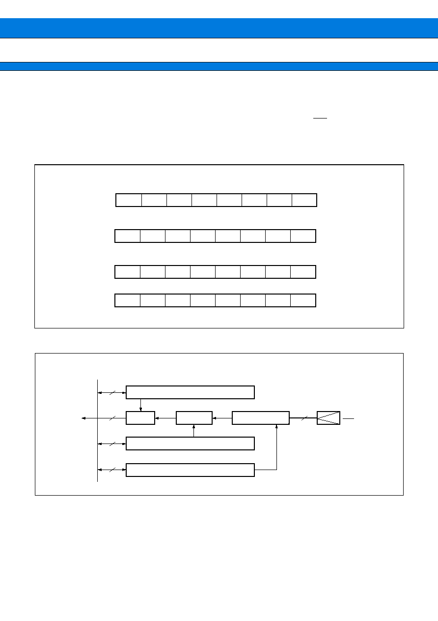
MB91307 Series
52
2.
External Interrupt - NMI Control Block
(1) Overview
The External Interrupt-control block controls external interrupt requests input at the NMI and INT0 to INT7 pins.
The request level can be selected from "H," "L," "rising edge," or "falling edge" detection (except for NMI).
(2) Register List
(3) Block Diagram
· External interrupt enable register (ENIR)
· External interrupt source register (EIRR)
· Request level setting register (ELVR)
bit
bit
bit
bit
7
6
5
4
3
2
1
0
EN6
EN7
EN5
EN4
EN3
EN2
EN1
EN0
15
14
13
12
11
10
9
8
ER6
ER7
ER5
ER4
ER3
ER2
ER1
ER0
15
14
13
12
11
10
9
8
LA7
LB7
LB6
LA6
LB5
LA5
LB4
LA4
7
6
5
4
3
2
1
0
LA3
LB3
LB2
LA2
LB1
LA1
LB0
LA0
9
9
INT0 to INT7
NMI
8
8
8
R-bus
Interrupt
request
Interrupt enable register
Gate
Source F/F
Edge detection circuit
Interrupt source register
Interrupt level setting register

MB91307 Series
53
3.
REALOS Related Hardware
REALOS related hardware is used by the REALOS operating system. Therefore, when REALOS is in use, these
resources cannot be used by user programs.
·
Delay Interrupt Module
(1) Overview
The delay interrupt module is a module that generates interrupts for task switching. This module can be used
with software instructions to generate and cancel interrupts to the CPU.
(2) Register List
(3) Block Diagram
Address :
7
bit
6
5
4
3
2
1
0
[R/W]
DLYI
DICR
00000044
H
DLYI
R-bus
Interrupt request

MB91307 Series
54
·
Bit Search Module
(1) Overview
Searches data written to input registers for "0" or "1" or change points, and outputs the value of the detected bits.
(2) Register List
(3) Block Diagram
Address :
0 detection data register
Address :
1 detection data register
Address :
Change point detection register
Address :
Detection results register
31
BSD0
BSD1
BSDC
BSRR
000003F0
H
000003F4
H
000003F8
H
000003FC
H
0
D-bus
Address
decoder
Input latch
Detection
mode
1 detection data capture
Bit search circuit
Search results

MB91307 Series
55
4.
16-bit Reload Timer
(1) Overview
The 16-bit timer is configured from a 16-bit down-counter, 16-bit reload register, prescaler for internal count clock
generation, and a control register.
For the input clock signal, a selection of three internal clock signals (machine clock multiplied by 2, 8, or 32) or
external clock is provided.
The output pin (TOUT) produces a toggle output waveform at every underflow in reload mode, and a square
wave indicating counting in progress in one-shot mode.
The input pin (TIN) can be used for event input in external event count mode, and trigger input or gate input in
internal clock mode.
The external event count function can be used in reload mode or as a frequency multiplier in external clock mode.
The MB91306R/MB91307R contain 3 channels (0 to 2) of this timer.
(2) Register List
· Control status register (TMCSR)
· 16-bit timer register (TMR)
· 16-bit reload register (TMRLR)
15
14
13
12
11
10
9
8
CSL1
CSL0
MOD2
MOD1
7
6
5
4
3
2
1
0
MOD0
OUTL
RELD
INTE
UF
CNTE
TRG
15
0
15
0

MB91307 Series
56
(3) Block Diagram
RELD
OUTE
OUTL
INTE
UF
CNTE
TRG
OUT
CTL.
CSL1
CSL0
MOD2
MOD1
MOD0
16
8
16
2
3
2
IN CTL.
2
2
2
1
3
5
3
EXCK
GATE
2
IRQ
R-bus
16-bit reload register
16-bit down counter
Reload
Clock selector
Re-trigger
Prescaler
clear
Internal clock
Port (TIN)
Port (TOT)

MB91307 Series
57
5.
U-TIMER (16 bit timer for UART baud rate generation)
(1) Overview
The U-TIMER is a 16-bit timer used to generate the baud rate for the UART. Any desired baud rate can be set
using the combination of chip operating frequency and U-TIMER reload value.
The U-TIMER can also be used as an interval timer by generating an interrupt from a count underflow event.
This device features a 3-channel built-in U-TIMER. By connecting two U-TIMER channels used as interval timers
in a cascade connection, it is possible to count intervals up to a maximum of 2
32
×
.
The available case connections are channel 0 to channel 1, and channel 1 to channel 2.
(2) Register List
(3) Block Diagram
UTIMR
UTIM
UTIMC
(W)
(R)
(R/W)
15
0
8 7
UTIMR (reload register)
UTIM (timer)
Clock
Load
Underflow
Under flow U-TIMER 1
To UART
control
f.f.
15
15
0
0
MUX
Channel 0 only
(Peripheral clock)

MB91307 Series
58
6.
UART
(1) Overview
The UART is an I/O port for asynchronous (start-stop synchronized) or CLK synchronized transmission, providing
the following features. This device features a 3-channel built-in UART.
· Full duplex double buffer
· Asynchronous (start-stop synchronized) or CLK synchronized transmission enabled
· Supports multi-processor mode
· Fully programmable baud rate
Built-in timer can be set to any desired baud rate (see U-TIMER description)
· Independent baud rate setting from external clock enabled.
· Error detection functions (parity, framing, overrun)
· Transfer signal NRZ encoded
· DMA transfer start from interrupt enabled
· DMAC interrupt source cleared by write operation to DRCL register.
(2) Register List
· Serial input register/Serial output registe (SIDR/SODR)
· Serial status register (SSR)
· Serial mode register (SMR)
· Serial control register (SCR)
· DRCL register (DRCL)
SIDR (R)/SODR (W)
SMR
SCR
(R/W)
(R/W)
(W)
SSR
DRCL
8 bit
8 bit
15
0
8 7
7
6
5
4
3
2
1
0
D6
D7
D5
D4
D3
D2
D1
D0
7
6
5
4
3
2
1
0
ORE
PE
FRE
RDRF
TDRE
RIE
TIE
7
6
5
4
3
2
1
0
MD0
MD1
CS0
SCKE
7
6
5
4
3
2
1
0
P
PEN
SBL
CL
A/D
REC
RXE
TXE
7
6
5
4
3
2
1
0

MB91307 Series
59
(3) Block Diagram
MD1
MD0
CS0
SCKE
SOE
PEN
P
SBL
CL
A
/
D
REC
RXE
TXE
PE
ORE
FRE
RDRF
TDRE
RIE
TIE
R-bus
SIDR
SODR
Control signal
From U-TIMER
External clock
SC
Clock select
circuit
Receiving status
decision circuit
DMA receiving
error signal
(to DMAC)
RX clock
RX control circuit
Start bit detect
circuit
Receiving bit
counter
Receiving parity
counter
Receiving shifter
Receiving
end
TX clock
RX interrupt
(to CPU)
TX interrupt
(to CPU)
TX control circuit
Sent start
circuit
Sending bit
counter
Sending parity
counter
Sending shifter
Sending
start
SMR
register
Control signal
SCR
register
SSR
register
SC (clock)
SI (receiving data)
SO (Sending data)

MB91307 Series
60
7.
A/D Converter (Sequential comparison type)
(1) Overview
This A/D converter is a module that coverts analog input voltages to digital values, and provides the following
features.
· Minimum conversion time 5.4
µ
s/ch (at machine clock 33 MHz-CKLP)
· Built-in sample & hold circuit
· Resolution 10 bits (8-bit accuracy)
· Analog input: 4 channels by program selection
Single conversion mode: Conversion on 1 select channel
Scan conversion mode: Select continuous multiple channels. Up to 4 channels can be selected by program.
Continuous conversion mode: Continuous conversion on selected channel
Stop conversion mode: 1-channel conversion then pause and wait until the next start is applied
(enables synchronized conversion start)
· DMA transfer start from interrupt enabled
· Start sources can be selected from software, external trigger (falling edge), reload timer (rising edge).
(2) Register List
· Control status register (ADCS)
· Data register (ADCR)
bit
bit
bit
bit
15
14
13
12
11
10
9
8
INT
BUSY
INTE
PAUS
STS1
STS0
STRT
7
6
5
4
3
2
1
0
MD0
MD1
ANS2
ANS1
ANS0
ANE2
ANE1
ANE0
15
14
13
12
11
10
9
8
9
8
7
6
5
4
3
2
1
0
6
7
5
4
3
2
1
0

MB91307 Series
61
(3) Block Diagram
(4) Precautions for Use:
When the A/D converter is started from an external trigger or internal timer, the ADCS register A/D start source
bits STS1, STS0 are set, and at this time the input values for the external trigger and internal timer should be
set to the inactive side. If these values are set to the active side, abnormal operation may result.
When setting the STS1, STS0 bits, set ATG = "1" input, reload timer (channel 2) = "0" output.
Note : If internal impedance is higher than the specified value, it may not be possible to obtain analog input
value sampling within the specified sampling time, so that proper results will not be obtained.
AV
CC
AVRH
AV
SS
R-bus
Input switch
Sample & hold circuit
Channel decoder
Internal voltage
Sequential
Data register (ADCR)
AD control register
ATG (External pin trigger)
Reload timer ch1 (Internal connection)
Timing generator
Prescaler
Clock (CLKP)

MB91307 Series
62
8.
I
2
C Interface
(1) Overview
The I
2
C interface operates as a master/slave device on the I
2
C bus at serial I/O ports with IC bus support. The
following features are provided.
· Master/slave sending and receiving
· Arbitration function
· Clock synchronization function
· Slave address/general call address detection function
· Transfer direction detection function
· Start condition repeat generation and detection function
· Bus error detection function
· 10-bit/7-bit master/slave addressing
· Compatible with standard mode (Max 100 Kbps) or high speed mode (Max 400 Kbps)
· Transfer end interrupt/bus error interrupt generation
(2) Register List
(Continued)
·
Bus Control Register (IBCR)
·
Bus Status Register (IBSR)
·
10-Bit Slave Address Register
Address : 000094
H
Default value
Address : 000095
H
Default value
Address : 000096
H
Default value
Address : 000097
H
Default value
R/W
0
R/W
0
R/W
0
R/W
0
R/W
0
R/W
0
R/W
0
15
14
13
12
11
10
9
8
BEIE
R/W
0
BER
SCC
MSS
ACK
GCAA
INTE
INT
R
0
R
0
R
0
R
0
R
0
R
0
R
0
7
6
5
4
3
2
1
0
RSC
R
0
BB
AL
LRB
TRX
AAS
GCA
ADT
R/W
0
R/W
0
15
14
13
12
11
10
9
8
TA9
TA8
R/W
0
R/W
0
R/W
0
R/W
0
R/W
0
R/W
0
R/W
0
7
6
5
4
3
2
1
0
TA6
R/W
0
TA7
TA5
TA4
TA3
TA2
TA1
TA0

MB91307 Series
63
(Continued)
· 10-Bit Slave Address Mask Register (ITMK)
· 7-Bit Slave Address Register (ISBA)
· 7-Bit Slave Address Mask Register (ISMK)
· Data Register (IDAR)
· Clock Control Register (ICCR)
· Clock Disable Register (IDBL)
Address : 000098
H
Default value
Address : 000099
H
Default value
Address : 00009B
H
Default value
Address : 00009A
H
Default value
Address : 00009D
H
Default value
Address : 00009E
H
Default value
Address : 00009F
H
Default value
R
0
R/W
1
R/W
1
15
14
13
12
11
10
9
8
RAL
R/W
0
ENTB
TM9
TM8
R/W
1
R/W
1
R/W
1
R/W
1
R/W
1
R/W
1
R/W
1
7
6
5
4
3
2
1
0
TM6
R/W
1
TM7
TM5
TM4
TM3
TM2
TM1
TM0
R/W
0
R/W
0
R/W
0
R/W
0
R/W
0
R/W
0
R/W
0
7
6
5
4
3
2
1
0
SA6
SA5
SA4
SA3
SA2
SA1
SA0
R/W
1
R/W
1
R/W
1
R/W
1
R/W
1
R/W
1
R/W
1
15
14
13
12
11
10
9
8
SM6
R/W
0
ENSB
SM5
SM4
SM3
SM2
SM1
SM0
R/W
0
R/W
0
R/W
0
R/W
0
R/W
0
R/W
0
R/W
0
7
6
5
4
3
2
1
0
D6
R/W
0
D7
D5
D4
D3
D2
D1
D0
R/W
0
R/W
1
R/W
1
R/W
1
R/W
1
R/W
1
15
14
13
12
11
10
9
8
W
0
TEST
EN
CS4
CS3
CS2
CS1
CS0
R/W
0
7
6
5
4
3
2
1
0
DBL

MB91307 Series
64
(3) Block Diagram
ICCR
EN
IDBL
DBL
ICCR
IBSR
BB
RSC
LRB
Last Bit
TRX
ADT
AL
IBCR
BER
BEIE
INTE
INT
IBCR
SCC
MSS
ACK
GCAA
IBSR
IDAR
AAS
GCA
ENTB
ISMK
RAL
ITBA
ITMK
ISBA
ISMK
CS4
CS3
CS2
CS1
CS0
2 3 4 5
32
Sync
First Byte
IRQ
SCL
SDA
R-b
us
I
2
C operation enabled
Clock enabled
Clock multiplier 2
Clock select 2 (1/12)
Bus busy
Repeat start
TX/RX
Start - stop
condition generator
Arbitration lost detector
Interrupt request
Start
Master
ACK OK
GC-ACK OK
Slave
Global call
Slave address
compare
End
Error
Shift clock
edge change
Start - stop
condition detector
Shift clock generator

MB91307 Series
65
9.
DMAC (DMA Controller)
(1) Overview
This module is used to accomplish DMA (Direct Memory Access) transfer on FR family devices.
DMA transfer controlled by this module increases system performance by enabling high speed transfer of many
types of data without going through the CPU.
·
Hardware Configuration
This module is principally configured from the following units:
· Five independent DMA channels
· 5 channels independent access control circuit
· 32-bit address registers (reload enabled: 2 per channel)
· 16-bit transfer count registers (reload enabled: 2 per channel)
· 4-bit block count registers (1 per channel)
· External transfer request input pins: DREQ0,DREQ1,DREQ2 (ch0, ch1, ch2 only)
· External transfer request acknowledge output pins: DACK0,DACK1,DACK2 (ch0, ch1, ch2 only)
· DMA output completed pins: DEOP0,DEOP1,DEOP2 (ch0, ch1, ch2 only)
· Fly-by transfer (memory to I/O, memory to memory) (ch0, ch1, ch2 only)
· Two-cycle transfer
·
Principal Functions
Data transfer using the DMAC module primarily involves the following functions:
· Supports independent data transfer on multiple channels (5 channels)
(1) Order of priority (ch0
>
ch1
>
ch2
>
ch3
>
ch4)
(2) The order can be reversed between ch0 and ch1.
(3) DMAC startup sources
·
Input from an external-only pin (edge detection/level detection, ch0, ch1, ch2 only)
·
Request from a built-in peripheral (shared interrupt request, including external interrupts)
·
Software request (register write)
(4) Transfer modes
·
Demand transfer / burst transfer / step transfer / block transfer
·
Addressing mode 32-bit full address designation (increment/decrement/fixed)
(address increment can be specified up to -255 to +255)
·
Data type, byte / half-word / word length
·
Single-shot / reload selection available

MB91307 Series
66
(2) Register Descriptions
ch0 Control/status register A
ch0 Control/status register B
ch1 Control/status register A
ch1 Control/status register B
ch2 Control/status register A
ch2 Control/status register B
ch3 Control/status register A
ch3 Control/status register B
ch4 Control/status register A
ch4 Control/status register B
Overall control register
ch0 Transfer source address register
ch0 Transfer source address register
ch1 Transfer source address register
ch1 Transfer source address register
ch2 Transfer source address register
ch2 Transfer source address register
ch3 Transfer source address register
ch3 Transfer source address register
ch4 Transfer source address register
ch4 Transfer source address register
(bit)
31
24
23
16
15
08
07
00
0000200
H
0000204
H
0000208
H
000020C
H
0000210
H
0000214
H
0000218
H
000021C
H
0000220
H
0000224
H
0000240
H
0001000
H
0001004
H
0001008
H
000100C
H
0001010
H
0001014
H
0001018
H
000101C
H
0001020
H
0001024
H
DMACA0
DMACB0
DMACA1
DMACB1
DMACA2
DMACB2
DMACA3
DMACB3
DMACA4
DMACB4
D M A C R
DMASA0
DMADA0
DMASA1
DMADA1
DMASA2
DMADA2
DMASA3
DMADA3
DMASA4
DMADA4

MB91307 Series
67
(3) Block Diagram
Read
Write
DDNO
BLK register
DDNO register
DTCR
DSS3 to DSS0
ERIR, EDIR
TYPE, MOD, WS
IRQ4 to
IRQ0
MCLREQ
X-bus
DADM, DASZ7 to DASZ0 DADR
SDAM, SASZ7 to SASZ0 SADR
DMA transfer request to
bus controller
Read/write
control
To bus
controller
Bus control block
Access
address
Address counter
Counter/buffer
C
ounter/buffer
Selector
Selector
Write back
Selector
Buffer
Counter
Selector
Write back
DTC two-stage register
Buffer
Counter
Selector
DMA start
source selection
circuit & request
acceptance
control
Priority
circuit
Status
transition
circuit
DMA controller
DDAD two-stage register
DDAD two-stage register
Bus control block
Peripheral start request/stop
input
External pin start request/stop
input
To interrupt controller
Peripheral interrupt clear
DMAC 5-channel Block Diagram
Write back

MB91307 Series
68
10. External Interface
(1) Overview
The external interface controller controls the interface between the LSI's internal bus and external memory or I/
O devices.
This section describes the functions of the external interface.
(2) Features
· Up to 32 bit-length (4G bytes space) address output.
· Connects directly to many external memory (8 bit/16 bit) devices, allows control of multiple access timings.
Asynchronous SRAM, asynchronous ROM/Flash memory (multiple write strobe type or byte enable type)
Page mode ROM/flash memory (2/4/8 page size enabled)
Burst ROM/Flash memory (MBM29BL160D/161D/162D etc.)
Address/data multiplexed bus (8 bit/16 bit width only)
Synchronous memory* (ASIC built-in memory etc.)
*: Does not connect to synchronous SRAM.
· 8 independent bank (chip select area) settings, each with corresponding chip select output available
Each area size can be set in multiples of 64K bytes (from 64K bytes to 2G bytes per chip select area).
Each area can be set in any desired area of logic address space (boundaries limited by area size).
· The following functions can be independently set for each chip select area.
Chip select area enable/disable (no access to prohibited areas)
Access timing type for each area, etc.
Detailed access timing settings (individual access type settings for wait cycle, etc.)
Data bus width setting (8 bit/16 bit)
Byte ordering endian setting* (big or little).
*: CS0 area available with big endian only.
Write prohibited setting (read-only areas)
Internal cache loading enable/disable settings
Pre-fetch function enable/disable settings
Maximum burst length setting (1,2,4,8)
· Different detailed timing settings for each access timing type
Different settings can be used for each chip select area even for the same access timing type.
Auto wait setting up to 15 cycles (asynchronous SRAM, ROM, Flash, I/O areas)
Bus cycle extension with external RDY input enabled (asynchronous SRAM, ROM, Flash, I/O areas)
First access wait and page wait settings enabled (burst, page mode ROM/FLASH areas)
Different idle, recovery cycles setup delay insertion etc. enabled
· Fly-by transfer with DMA enabled
Transfer between memory and I/O with 1 access
Memory wait cycle can be synchronized with I/O wait cycle during fly-by
Hold time can be obtained by delaying transfer access only
Specific idle/recovery cycles can be set for fly-by transfer
· External bus arbitration using BRQ and BGRNT enabled
· Pins not used in external interface can be set for use as general purpose I/O ports

MB91307 Series
69
(3) Block Diagram
(4) I/O Pins
These are the external interface pins. (Some pins have dual functions.)
< Normal bus interface >
A24 to A0, D31 to D16
CS0, CS1, CS2, CS3, CS4, CS5, CS6, CS7
AS, SYSCLK, MCLK
RD
WE, WR0 (UUB) , WR1 (ULB)
RDY, BRQ, BGRNT
< Memory interface >
MCLK
LBA (
=
AS) , BAA*
*: For burst ROM, Flash use
MUX
CS0 to CS7
RD
WR0, WR1
AS, BAA
BRQ
BGRNT
RDY
32
32
Write buffer
Read buffer
Switch
Switch
+
1 or
+
2
Address buffer
ASR
ASZ
Comparator
Data block
Address block
Resisters &
controls
External pin control block
All block control
Internal
address bus
Internal data
bus
External data bus
External address bus

MB91307 Series
70
< DMA interface >
IOWR, IORD
DACK0, DACK1, DACK2
DREQ0, DREQ1, DREQ2
DEOP0/DSTP0, DEOP1/DSTP1, DEOP2/DSTP2
(5) Register List
Reserved: This address is reserved, and should always be set to "0."
MODR: Cannot be accessed from user programs.
Address 31
24 23
16 15
08 07
00
00000640
H
ASR0
ACR0
00000644
H
ASR1
ACR1
00000648
H
ASR2
ASR2
0000064C
H
ASR3
ACR3
00000650
H
ASR4
ACR4
00000654
H
ASR5
ACR5
00000658
H
ASR6
ACR6
0000065C
H
ASR7
ACR7
00000660
H
AWR0
AWR1
00000664
H
AWR2
AWR3
00000668
H
AWR4
AWR5
0000066C
H
AWR6
AWR7
00000670
H
Reserved
Reserved
Reserved
Reserved
00000674
H
Reserved
Reserved
Reserved
Reserved
00000678
H
IOWR0
IOWR1
IOWR2
Reserved
0000067C
H
Reserved
Reserved
Reserved
Reserved
00000680
H
CSER
CHER
Reserved
TCR
00000684
H
Reserved
Reserved
Reserved
Reserved
00000688
H
Reserved
Reserved
Reserved
Reserved
0000068C
H
Reserved
Reserved
Reserved
Reserved
·
·
·
·
·
·
·
·
·
·
·
·
·
·
·
000007F8
H
Reserved
Reserved
Reserved
Reserved
000007FC
H
Reserved
(MODR)
Reserved
Reserved

MB91307 Series
71
ELECTRICAL CHARACTERISTICS
1.
Absolute Maximum Ratings
*1 : The parameter is based on V
SS
=
AV
SS
=
0 V.
*2 : V
CC
must not be lower than V
SS
-
0.3 V.
*3 : AV
CC
and AVRH shall never exceed V
CC
+
0.3 V. Also AVRH shall never exceed AV
CC
.
*4 : Maximum output current determines the peak value of any one of the corresponding pins.
*5 : Average output current is defined as the value of the average current flowing over 100 ms at any one of the
corresponding pins.
*6 : Average total output current is defined as the value of the average current flowing over 100 ms at all of the
corresponding pins.
*7 :
·
Applicable to pins : P20 to P27, P60 to P67, P70, PJ0 to PJ7, PI0 to PI5, PH0 to PH7, PB0 to PB5, PA0 to
PA7, P80 to P82, P85, P90 to P97, AN0 to AN3
·
Use within recommended operating conditions.
·
Use at DC voltage (current) .
·
The +B signal should always be applied with a limiting resistance placed between the +B signal and the
microcontroller.
·
The value of the limiting resistance should be set so that when the +B signal is applied the input current to
the microcontroller pin does not exceed rated values, either instantaneously or for prolonged periods.
Parameter
Symbol
Rating
Unit
Remarks
Min
Max
Supply voltage*
1
V
CC
V
SS
-
0.5
V
SS
+
4.0
V
*2
Internal supply voltage
V
CCI
V
SS
-
0.5
V
SS
+
2.2
V
*2
Analog supply voltage
AV
CC
V
SS
-
0.5
V
SS
+
4.0
V
*3
Analog reference voltage
AVRH
V
SS
-
0.5
V
SS
+
4.0
V
*3
Input voltage*
1
V
I
V
SS
-
0.3
V
CC
+
0.3
V
*8
Analog pin input voltage
V
IA
V
SS
-
0.3
AV
CC
+
0.3
V
Output voltage*
1
V
O
V
SS
-
0.3
V
CC
+
0.3
V
*8
Maximum clamp current
I
CLAMP
-
2.0
2.0
mA
*7
Total maximum clamp current
I
CLAMP
20
mA
*7
L level maximum output current
I
OL
10
mA
*4
L level average output current
I
OLAV
8
mA
*5
L level maximum total output current
I
OL
100
mA
L level average total output current
I
OLAV
50
mA
*6
H level maximum output current
I
OH
-
10
mA
*4
H level average output current
I
OHAV
-
4
mA
*5
H level maximum total output current
I
OH
-
50
mA
H level average total output current
I
OHAV
-
20
mA
*6
Power consumption
P
D
750
mW
Operating temperature
T
A
0
+
70
°
C
Storage temperature
T
STG
+
150
°
C

MB91307 Series
72
·
Note that when the microcontroller drive current is low, such as in the power saving modes, the +B input
potential may pass through the protective diode and increase the potential at the VCC pin, and this may affect
other devices.
·
Note that if a +B signal is input when the microcontroller current is off (not fixed at 0 V), the power supply is
provided from the pins, so that incomplete operation may result.
·
Note that if the +B input is applied during power-on, the power supply is provided from the pins and the
resulting supply voltage may not be sufficient to operate the power-on reset.
·
Care must be taken not to leave the +B input pin open.
·
Note that analog system input/output pins other than the A/D input pins (LCD drive pins, comparator input
pins, etc.) cannot accept +B signal input.
·
Sample recommended circuits :
*8 : V
I
and V
O
must never exceed V
CC
+
0.3 V. However if the maximum current to/from an input is limited by some
means with external components, the I
CLAMP
rating supersedes the V
I
rating.
WARNING: Semiconductor devices can be permanently damaged by application of stress (voltage, current,
temperature, etc.) in excess of absolute maximum ratings. Do not exceed these ratings.
V
CC
P-ch
N-ch
R
·
Input/Output Equivalent circuits
+
B input (0 V to 16 V)
Protective diode
Limiting
resistance

MB91307 Series
73
2.
Recommended Operating Conditions
(V
SS
=
AV
SS
=
0 V)
WARNING: The recommended operating conditions are required in order to ensure the normal operation of the
semiconductor device. All of the device's electrical characteristics are warranted when the device is
operated within these ranges.
Always use semiconductor devices within their recommended operating condition ranges. Operation
outside these ranges may adversely affect reliability and could result in device failure.
No warranty is made with respect to uses, operating conditions, or combinations not represented on
the data sheet. Users considering application outside the listed conditions are advised to contact their
FUJITSU representatives beforehand.
Parameter
Symbol
Value
Unit
Remarks
Min
Max
Supply voltage
V
CC
3.0
3.6
V
V
CCI
1.65
1.95
V
Analog supply voltage
AV
CC
V
SS
-
0.3
V
SS
+
3.6
V
Analog reference voltage
AVRH
AV
SS
AV
CC
V
Operating temperature
T
A
0
+
70
°
C

MB91307 Series
74
3.
DC Characteristics
(V
CCI
=
1.65 V to 1.95 V, V
CC
=
3.0 V to 3.6 V, V
SS
=
AV
SS
=
0 V, T
A
=
0
°
C to
+
70
°
C)
* : Pins without hysteresis input pins: D16 to D31, RDY, BRQ, INIT
Parameter
Symbol
Pin name
Condition
Value
Unit
Remarks
Min
Typ
Max
"H" level input
voltage
V
IH
See note *
0.7
×
V
CC
V
CC
+
0.3
V
V
HIS
Input pins
other than *
0.8
×
V
CC
V
CC
+
0.3
V
Hysteresis
input
"L" level input
voltage
V
IL
See note *
V
SS
0.25
×
V
CC
V
V
ILS
Input pins
other than *
V
SS
0.2
×
V
CC
V
Hysteresis
input
"H" level output
voltage
V
OH
D16 to D31
A00 to A25
P6 to PH
V
CC
=
3.0 V
I
OH
=
-
4.0 mA
V
CC
-
0.5
V
CC
V
"L" level output
voltage
V
OL
D16 to D31
A00 to A25
P6 to PH
V
CC
=
3.0 V
I
OL
=
8.0 mA
V
SS
0.4
V
Input leak
current
(Hi-Z output leak
current)
I
LI
D16 to D31
A00 to A25
P8 to PH
V
CC
=
3.6 V
0.45 V<V
I
<V
CC
-
5
+
5
µ
A
Pull-up resistance
R
UP
INIT
V
CC
=
3.6 V
V
I
=
0.45 V
12
25
100
k
Pull-down
resistance
R
DOWN
P82/BRQ
V
CC
=
3.6 V
V
I
=
3.3 V
12
25
100
k
Supply current
I
CC
V
CC
+
V
CCI(
f
C
=
16.5 MHz
V
CC
=
3.3 V
V
CCI
=
1.8 V
150
mA
(4x
multiplied)
66 MHz
operation
I
CCS
f
C
=
16.5 MHz
V
CC
=
3.3 V
V
CCI
=
1.8 V
50
mA
Sleep mode
I
CCH
T
A
=
25
°
C
V
CC
=
3.3 V
V
CCI
=
1.8 V
150
µ
A
Stop mode
Input capacitance
C
IN
Other than:
V
CC
V
SS
AV
CC
AV
SS
5
15
pF
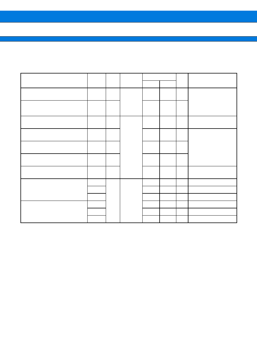
MB91307 Series
75
4.
AC Characteristics
(1) Clock Timing Standards
(V
CCI
=
1.65 V to 1.95 V, V
CC
=
3.0 V to 3.6 V, V
SS
=
AV
SS
=
0 V, T
A
=
0
°
C to
+
70
°
C)
*1 : When using the PLL, the clock frequency should be around 12.5 to 16.5 MHz.
*2 : The values shown represent a minimum clock frequency of 12.5 MHz input at the X0 pin, using the oscillator
circuit PLL and a gear ratio of 1/16.
Parameter
Symbol
Pin
name
Condi-
tion
Value
Unit
Remarks
Min
Max
Clock frequency (1)
f
C
X0
X1
12.5
16.5
MHz
PLL system*
1
(self oscillation
16.5MHz,multiplied
x4,maximum internal
operation 66MHz)
Clock cycle time
t
C
X0
X1
60.6
ns
Clock frequency (2)
f
C
X0
X1
10
33
MHz
Self oscillation (x1/2
frequency input)
Clock frequency (3)
f
C
X0
X1
10
33
MHz
External clock
Clock cycle time
t
C
X0
X1
40
100
ns
Input clock pulse width
P
WH
P
WL
X0
X1
16
ns
Input clock rise, fall time
t
CR
t
CF
X0
X1
8
ns
(t
CR
+
t
CF
)
Internal operating clock frequency
f
CP
0.78
*2
66
MHz CPU system
f
CPP
0.78
*2
33
MHz Peripheral system
f
CPT
0.78
*2
66
MHz External bus system
Internal operating clock cycle time
t
CP
15.2
1280
*2
ns
CPU system
t
CPP
30.3
1280
*2
ns
Peripheral system
t
CPT
15.2
1280
*2
ns
External bus system

MB91307 Series
76
·
Clock timing measurement conditions:
·
Warranted operating range
·
External/internal clock setting range
Notes : · When using the PLL, the external clock input should be around 16.5 MHz.
· Set PLL oscillator stabilization time > 300
µ
s.
· The internal clock gear setting should be within the values shown in (1) clock timing standards.
0.8 V
CC
0.2 V
CC
t
CF
t
CR
t
C
P
WH
P
WL
C
=
50 pF
Output pin
0
(MHz)
1.95
1.65
f
CP
/ f
CPP
66
33
0.78
V
CC
(V)
Internal clock
Power supply
Warranted operating temperature:
(T
A
=0
°
C to +70
°
C)
f
CPP
is represented by the shaded area
66
(MHz)
33
16.5
4 : 4
2 : 2
1 : 2
f
CP
,
f
CPT
f
CPP
Internal clock
CPU: Divided ratio for peripherals
Peripheral system
CPU, external bus systems

MB91307 Series
77
(2) Clock Output Timing
(V
CCI
=
1.65 V to 1.95 V, V
CC
=
3.0 V to 3.6 V, V
SS
=
AV
SS
=
0 V, T
A
=
0
°
C to
+
70
°
C)
*1 : t
CYC
represents the frequency of one clock cycle including the gear period.
*2 : The values shown represent standards for
×
1 gear period.
For gear period settings of 1/2, 1/4, 1/8, use the following formula replacing n with the value 1/2, 1/4, 1/8
respectively.
(1/2
×
1/n)
×
t
CYC
-
10
*3 : The values shown represent standards for
×
1 gear period.
Note : t
CPT
indicates the internal operating clock time. See " (1) Clock Timing Standards".
Parameter
Symbol
Pin
name
Conditions
Value
Unit
Remarks
Min
Max
Cycle time
t
CYC
MCLK,
SYSCLK
t
CPT
ns
*1
MCLK
MCLK
SYSCLK
SYSCLK
t
CHCL
MCLK,
SYSCLK
1/2
×
t
CYC
-
3
1/2
×
t
CYC
+
3
ns
*2
MCLK
MCLK
SYSCLK
SYSCLK
t
CLCL
MCLK,
SYSCLK
1/2
×
t
CYC
-
3
1/2
×
t
CYC
+
3
ns
*3
MCLK,
SYSCLK
V
OH
V
OL
V
OH
t
CYC
t
CLCH
t
CHCL

MB91307 Series
78
(3) Reset and Hardware Standby Input Standards
(V
CCI
=
1.65 V to 1.95 V, V
CC
=
3.0 V to 3.6 V, V
SS
=
AV
SS
=
0 V, T
A
=
0
°
C to
+
70
°
C)
* : INIT input time (at power-on)
FAR, Ceralock :
×
2
15
or greater recommended
Crystal
:
×
2
21
or greater recommended
: Power on
X0/X1 period
×
2
Note : t
CP
indicates the clock cycle time. See " (1) Clock Timing Standards".
Parameter
Symbol
Pin
name
Conditions
Value
Unit
Remarks
Min
Max
Hardware standby input time
t
HSTL
V
CCI
t
CP
×
5
ns
INIT input time
(power-on)
t
INTL
INIT
*
ns
INIT input time
(other than power-on)
t
CP
×
5
ns
INIT
0.2 V
CC
t
RSTL
, t
HSTL
, t
INTL
HST

MB91307 Series
79
(4) Normal Bus Access Read/Write Operation
(V
CCI
=
1.65 V to 1.95 V, V
CC
=
3.0 V to 3.6 V, V
SS
=
AV
SS
=
0 V, T
A
=
0
°
C to
+
70
°
C)
* : To extend bus time by automatic wait insertion or RDY input, add to this value (t
CYC
×
number of extended cycles).
Note : t
CYC
indicates the cycle time. See " (2) Clock Output Timing".
Parameter
Symbol
Pin name
Condition
Value
Unit Remarks
Min
Max
CS0 to CS7 setup
t
CSLCH
MCLK, SYSCLK,
CS0 to CS7
3
ns
CS0 to CS7 hold
t
CSHCH
3
t
CYC
/2
+
6
ns
Address setup
t
ASCH
MCLK, SYSCLK,
A23 to A00
3
ns
Address hold
t
CHAX
MCLK, SYSCLK,
A23 to A00
3
t
CYC
/2
+
6
ns
Valid address
valid data input time
t
AVDV
A23 to A00,
D31 to D16
3/2
×
t
CYC
-
11
ns
*
WR0 to WR1 delay time
t
CHWL
MCLK, SYSCLK,
WR0 to WR1
6
ns
t
CHWH
6
ns
WR0 to WR1 minimum pulse
width
t
WLWH
WR0 to WR1
t
CYC
-
3
ns
Data setup
WRx
t
DSWH
WR0 to WR1,
D31 to D16
t
CYC
ns
WRx
data hold time
t
WHDX
5
ns
RD delay time
t
CHRL
MCLK, SYSCLK,
RD
6
ns
t
CHRH
6
ns
RD
valid data input time
t
RLDV
RD,
D31 to D16
t
CYC
-
10
ns
*
Data setup
RD
time
t
DSRH
10
ns
RD
data hold time
t
RHDX
0
ns
RD minimum pulse width
t
RLRH
RD
t
CYC
-
3
ns
AS setup
t
ASLCH
MCLK, SYSCLK,
AS
3
ns
AS hold
t
ASHCH
3
ns
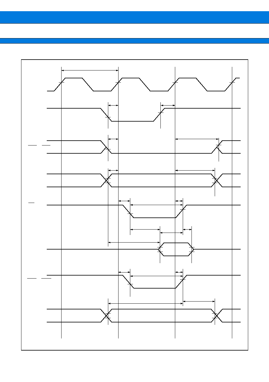
MB91307 Series
80
MCLK,
SYSCLK
AS
LBA
CS0 to CS7
V
OH
V
OH
V
OH
V
OL
V
OL
V
OH
V
OH
V
OL
V
OH
V
OL
V
OL
V
OL
A23 to A00
RD
D31 to D16
WR0 to WR1
D31 to D16
V
OH
V
OH
V
OL
V
OH
V
OH
V
OH
V
OL
V
OH
V
OL
V
OH
V
OL
V
OH
t
ASCH
t
AVDV
t
RLDV
t
DSRH
t
RHDX
t
WLWH
t
CHWL
t
CHWH
t
CHAX
t
CHRH
t
DSWH
t
WHDX
t
ASHCH
t
CYC
t
ASLCH
t
CSHCH
t
CHRL
t
RLRH
t
CSLCH
BA1
Write

MB91307 Series
81
(5) Ready Input Timing
(V
CCI
=
1.65 V to 1.95 V, V
CC
=
3.0 V to 3.6 V, V
SS
=
AV
SS
=
0 V, T
A
=
0
°
C to
+
70
°
C)
Parameter
Symbol
Pin name
Condition
Value
Unit
Remarks
Min
Max
RDY setup time
MCLK
, SYSCLK
t
RDYS
MCLK, SYSCLK,
RDY
10
ns
MCLK
, SYSCLK
RDY hold time
t
RDYH
MCLK, SYSCLK,
RDY
0
ns
MCLK,
SYSCLK
V
OH
V
OH
V
OL
V
OL
V
OL
V
OH
V
OL
V
OH
V
OH
V
OL
V
OH
V
OL
t
RDYH
t
RDYH
RDY
RDY
t
CYC
t
RDYS
t
RDYS
t
CHASL
Wait applied
Wait not applied

MB91307 Series
82
(6) Hold Timing
(V
CCI
=
1.65 V to 1.95 V, V
CC
=
3.0 V to 3.6 V, V
SS
=
AV
SS
=
0 V, T
A
=
0
°
C to
+
70
°
C)
Note: After a BRQ is accepted, a minimum of 1 cycle is required before BGRNT changes.
Parameter
Symbol
Pin name
Condition
Value
Unit
Remarks
Min
Max
BGRNT delay time
t
CHBGL
MCLK, SYSCLK,
BGRNT
3
13.5
ns
t
CHBGH
3
13.5
ns
Pin floating
BGRNT
time
t
XHAL
BGRNT
t
CYC
-
10
t
CYC
+
10
ns
BGRNT
valid time
t
HAHV
t
CYC
-
10
t
CYC
+
10
ns
MCLK,
SYSCLK
V
OH
t
CHBGL
V
OL
V
OH
V
OH
V
OH
V
OH
t
CHBGH
BRQ
BGRNT
t
CYC
t
HAHV
t
HXAL
Pins
High-Z

MB91307 Series
83
(7) UART Timing
(V
CCI
=
1.65 V to 1.95 V, V
CC
=
3.0 V to 3.6 V, V
SS
=
AV
SS
=
0 V, T
A
=
0
°
C to
+
70
°
C)
Notes: · Above ratings are for operation in CLK synchronized mode.
· t
CPP
is the cycle time of the peripheral system clock.
Parameter
Symbol
Pin name
Condition
Value
Unit
Remarks
Min
Max
Serial clock cycle time
t
SCYC
SC0 to SC2
Internal
shift lock
mode
8 t
CPP
ns
SCLK
SOUT delay time
t
SLOV
SC0 to SC2,
SO0 to SO2
-
80
80
ns
Valid SIN
SCLK
t
IVSH
SC0 to SC2,
SI0 to SI2
100
ns
SCLK
valid SIN hold time
t
SHIX
SC0 to SC2,
SI0 to SI2
60
ns
Serial clock "H" pulse width
t
SHSL
SC0 to SC2
External
shift lock
mode
4 t
CPP
ns
Serial clock "L" pulse width
t
SLSH
SC0 to SC2
4 t
CPP
ns
SCLK
SOUT delay time
t
SLOV
SC0 to SC2,
SO0 to SO2
150
ns
Valid SIN
SCLK
t
IVSH
SC0 to SC2,
SI0 to SI2
60
ns
SCLK
valid SIN hold time
t
SHIX
SC0 to SC2,
SI0 to SI2
60
ns
·
Internal Shift Clock Mode
·
External Shift Clock Mode
SC0, SC1
SO0, SO1
SI0, SI1
t
SCYC
t
SLOV
t
IVSH
t
SHIX
V
OL
V
OH
V
OL
V
OH
V
OL
V
OH
V
OL
V
OH
V
OL
SC0, SC1
SO0, SO1
SI0, SI1
t
SLOV
t
SLSH
t
SHSL
t
IVSH
t
SHIX
V
OH
V
OL
V
OH
V
OL
V
OL
V
OL
V
OH
V
OL
V
OH
V
OL

MB91307 Series
84
(8) Timer Clock Input Timing
(V
CCI
=
1.65 V to 1.95 V, V
CC
=
3.0 V to 3.6 V, V
SS
=
AV
SS
=
0 V, T
A
=
0
°
C to
+
70
°
C)
Note: t
CYCP
is the cycle time of the peripheral system clock.
(9) Trigger Input Timing
(V
CCI
=
1.65 V to 1.95 V, V
CC
=
3.0 V to 3.6 V, V
SS
=
AV
SS
=
0 V, T
A
=
0
°
C to
+
70
°
C)
Note: t
CYCP
is the cycle time of the peripheral system clock.
Parameter
Symbol
Pin name
Condition
Value
Unit
Remarks
Min
Max
Input pulse width
t
TIWH
t
TIWL
TIN0 to TIN2
2 t
CYCP
ns
Parameter
Symbol
Pin name
Condition
Value
Unit
Remarks
Min
Max
A/D startup trigger input time
t
ATGX
ATG
5 t
CYCP
ns
t
TIWH
t
TIWL
TIN0 to TIN2
ATG
t
ATGX,
t
INP
, t
PTG

MB91307 Series
85
(10) DMA Controller Timing
(V
CCI
=
1.65 V to 1.95 V, V
CC
=
3.0 V to 3.6 V, V
SS
=
AV
SS
=
0 V, T
A
=
0
°
C to
+
70
°
C)
Parameter
Symbol
Pin name
Condition
Value
Unit
Remarks
Min
Max
DREQ input pulse width
t
DRWH
DREQ 0 to DREQ2
5 t
CYC
ns
DSTP input pulse width
t
DSWH
DSTP 0 to DSTP2
5 t
CYC
ns
DACK delay time
t
CLDL
MCLK, SYSCLK,
DACK0 to DACK2
6
ns
t
CLDH
6
DEOP delay time
t
CLEL
MCLK, SYSCLK,
DEOP 0 to DEOP2
6
ns
t
CLEH
6
IORD delay time
t
CLIRL
MCLK, SYSCLK
6
ns
t
CLIRH
6
IOWR delay time
t
CLIWL
MCLK, SYSCLK
6
ns
t
CLIWH
6

MB91307 Series
86
MCLK,
SYSCLK
DACK0 to DACK2
DEOP0 to DEOP2
DREQ0 to DREQ2
DSTP0 to DSTP2
IORD
V
OL
V
OH
V
OL
V
OL
V
OH
V
OL
V
OH
V
OL
V
OH
V
OL
V
OH
V
OL
V
OH
V
OL
V
OH
V
OL
V
OH
t
CLEL
t
CLIRL
t
CLIWL
t
CLDL
t
CYC
t
CLEH
t
CLIRH
t
CLIWH
t
DRWH
t
DSWH
t
CLDH
BA1
BA2
IOWR

MB91307 Series
87
(11) I
2
C Timing
(V
CCI
=
1.65 V to 1.95 V, V
CC
=
3.0 V to 3.6 V, V
SS
=
AV
SS
=
0 V, T
A
=
0
°
C to
+
70
°
C)
*1 : R, C : Pull-up resistor and load capacitor of the SCL and SDA lines.
*2 : The maximum t
HDDAT
only has to be met if the device does not stretch the "L" width (t
LOW
) of the SCL signal.
*3 : A Fast-mode I
2
C-bus device can be used in a Standard-mode I
2
C-bus system, but the requirement
t
SUDAT
250 ns must then be met.
*4 : For use at over 100 kHz, set the resource clock to at least 6 MHz.
Parameter
Symbol
Condition
Standard mode
High-speed mode*
4
Unit
Min
Max
Min
Max
SCL clock frequency
f
SCL
R
=
1.0 k
,
C
=
50 pF*
1
0
100
0
400
kHz
(Repeat) "start" condition hold time
SDA
SCL
t
HDSTA
4.0
0.6
µ
s
SCL clock "L" width
t
LOW
4.7
1.3
µ
s
SCL clock "H" width
t
HIGH
4.0
0.6
µ
s
Repeat "start" condition setup time
SCL
SDA
t
SUSTA
4.7
0.6
µ
s
Data hold time
SCL
SDA
t
HDDAT
0
3.45*
2
0
0.9*
3
µ
s
Data setup time
SDA
SCL
t
SUDAT
250
100
ns
"Stop" condition setup time
SCL
SDA
t
SUSTO
4.0
0.6
µ
s
Bus free time between "stop" and
"start" conditions
t
BUS
4.7
1.3
µ
s
SDA
SCL
t
BUS
t
SUSTA
t
HDSTA
t
SUSTO
t
HIGH
t
HDDAT
t
HDSTA
t
LOW
t
SUDAT

MB91307 Series
88
5.
A/D Converter Electrical Characteristics
(V
CCI
=
1.65 V to 1.95 V, V
CC
=
+
3.0 V to
+
3.6 V, V
SS
=
AV
SS
=
0 V, T
A
=
0
°
C to
+
70
°
C)
*1 : At V
CC
= AV
CC
= 3.0 V to 3.6 V, V
CCI
=
1.65 V to 1.95 V machine clock 33 MHz.
*2 : Current in CPU stop mode with A/D converter not operating (at V
CC
= AV
CC
= AVRH = 3.6 V, V
CCI
=
1.95 V)
· About the external impedance of the analog input and its sampling time
· A/D converter with sample and hold circuit. If the external impedance is too high to keep sufficient sampling
time, the analog voltage charged to the internal sample and hold capacitor is insufficient, adversely affecting
A/D conversion precision.
Parameter Symbol
Pin
name
Value
Unit
Min
Typ
Max
Resolution
10
10
BIT
Total error
±
4.5
LSB
Linear error
±
3.0
LSB
Differential linear error
±
2.5
LSB
Zero transition error
V
OT
AN0 to AN3
-
1.5
+
0.5
+
4.5
LSB
Full scale transition error
V
FST
AN0 to AN3
AVRH
-
4.5
AVRH
-
1.5
AVRH
+
4.5
LSB
Conversion time
5.4 *
1
µ
s
Analog port input current
I
AIN
AN0 to AN3
0.1
10
µ
A
Analog input voltage
V
AIN
AN0 to AN3
AVss
AVRH
V
Reference voltage
AVRH
AVss
AV
CC
V
Supply current
I
A
AV
CC
600
µ
A
I
AH
10 *
2
µ
A
Reference voltage supply current
I
R
AVRH
600
µ
A
I
RH
10 *
2
µ
A
Inter-channel variation
AN0 to AN3
5
LSB
R
C
During sampling : ON
Analog input
Comparator
· Analog input circuit model
Note : The values are reference values.
R
C
MB91307R/306R
5.0 k
(Max) 15 pF (Max)
MB91V307R
8.1 k
(Max) 10 pF (Max)

MB91307 Series
89
· To satisfy the A/D conversion precision standard, consider the relationship between the external impedance
and minimum sampling time and either adjust the operating frequency or decrease the external impedance
so that the sampling time is longer than the minimum value.
· If the sampling time cannot be sufficient, connect a capacitor of about 0.1 mF to the analog input pin.
· About errors
As | AVRH | becomes smaller, values of relative errorsgrow larger.
0
MB91V307R
MB91307R
MB91306R
5
10
15
20
25
30
35
100
90
80
70
60
50
40
30
20
10
0
0
MB91V307R
MB91307R
MB91306R
1
2
3
4
5
6
8
20
18
16
14
12
10
8
6
4
2
0
7
External impedance
=
0 k
to 100 k
External impedance
=
0 k
to 20 k
External impedance [k
]
External impedance [k
]
Minimum sampling time [
µ
s]
Minimum sampling time [
µ
s]
·
The relationship between external impedance and minimum sampling time

MB91307 Series
90
Definition of A/D Converter Terms
· Resolution
Indicates the ability of the A/D converter to discriminate analog variation
· Linear error
Expresses the deviation between actual conversion characteristics and a straight line connecting the device's
zero transition point (00 0000 0000
00 0000 0001) and full scale transition point (11 1111 1110
11
1111 1111)
· Differential linear error
Expresses the deviation of the logical value of input voltage required to create a variation of 1 LSB in output
code.
3FF
H
3FE
H
3FD
H
004
H
003
H
002
H
001
H
AVRL
AVRH
{1 LSB
×
(N
-
1)
+
V
TO
}
V
NT
V
FST
V
TO
N
-
1
AVRL
AVRH
N
-
2
N
-
2
N
-
1
V
NT
V
(N
-
1)T
[Linear Error]
[Differential linear error]
Digital output
Digital output
Actual variation
(measured
value)
(measured
value)
Actual variation
Theoretical values
(measured value)
Analog input
Analog input
Theoretical
Actual variation
(measured
value)
(measured value)
Actual variation
Linear error in digital output N
=
V
NT
-
{1 LSB
×
(N
-
1)
+
V
OT
}
1 LSB
[LSB]
Differential linear error in digital output N
=
V (
N
+
1
)
T
-
V
NT
1 LSB
-
1
1 LSB
=
V
FST
-
V
OT
1022
[V]
1 LSB"
=
AVRH
-
AVRL
1024
[V]
V
OT
: Voltage at which the digital output transitions from "000"
H
to "001"
H
.
V
FST
: Voltage at which the digital output transitions from "3FE"
H
to "3FF"
H
.
V
NT
: Voltage at which the digital output transitions from (N-1) to N.
[LSB]
(theoretical value)

MB91307 Series
91
· Total error
Expresses the difference between actual and theoretical values as error, including zero transition error, full-
scale error, and linearity error.
3FF
H
3FE
H
3FD
H
004
H
003
H
002
H
001
H
AVRL
AVRH
1.5 LSB
V
NT
0.5 LSB
{1 LSB
×
(N
-
1)
+
0.5 LSB
[Total error]
Digital output
Actual variation
(measured
value)
Actual variation
theoretical value
Analog input
Total error in digital output N
=
V
NT
-
{1 LSB"
×
(N
-
1)
+
0.5 LSB"}
1 LSB"
[LSB]
V
OT
" (theoretical value)
=
AVRL
+
0.5 LSB" [V]
V
FST
" (theoretical value)
=
AVRH
-
1.5 LSB" [V]
V
NT
: Voltage at which digital output transitions from (N-1) to N.

MB91307 Series
92
EXAMPLE CHARACTERISTICS
(Continued)
(1) Sample output voltage characteristics (T
A
=
+
25
°
C)
(2) Sample input voltage characteristics (T
A
=
+
25
°
C)
(3) Sample supply current characteristics
Output voltage (V)
Supply voltage (V)
0.4
0.3
0.2
0.1
0.0
3.0
3.2
3.4
3.6
Supply voltage (V)
Output voltage (V)
3.6
3.4
3.2
3.0
2.8
3.0
3.2
3.4
3.6
Sample output H voltage (V
OH
) characteristics
Sample output L voltage (V
OL
) characteristics
3.0
2.0
1.0
0.0
3.0
3.2
3.4
3.6
V
IH
V
IL
Input voltage (V)
Supply voltage (V)
3.0
2.0
1.0
0.0
3.0
3.2
3.4
3.6
V
IH
V
IL
Supply voltage (V)
Input voltage (V)
Sample input H/L level characteristics (CMOS)
Sample input H/L level characteristics (hysteresis)
200
150
100
50
0
3.0
3.2
3.4
3.6
Supply current (mA)
Supply voltage (V)
200
150
100
50
0.0
0
25
70
Temperature (
°
C)
Supply current (mA)
Sample supply current (I
CC
) characteristics
(T
A
=
+
25
°
C, 66 MHz)
Sample supply current (I
CC
) characteristics
(V
CC
=
3.3 V, 66 MHz)
MB91307 Series
93
(Continued)
(4) Port resistance characteristics
Sample sleep current (I
CCS
) characteristics
(T
A
=
+
25
°
C, 33 MHz)
50
40
30
20
3.0
3.2
3.4
3.6
Supply current (mA)
Supply voltage (V)
Sample sleep current (I
CCS
) characteristics
(V
CC
=
3.3 V, 33 MHz)
50
40
30
20
0
25
70
Supply current (mA)
Temperature (
°
C)
Sample A/D supply current (I
A
) characteristics
(T
A
=
+
25
°
C, 33 MHz)
500
400
300
200
3.0
3.2
3.4
3.6
Supply current (
µ
A)
Supply voltage (V)
Sample A/D reference current (I
R
) characteristics
(T
A
=
+
25
°
C, 33 MHz)
500
400
300
200
3.0
3.2
3.4
3.6
Supply current (
µ
A)
Supply voltage (V)
30
25
20
15
3.0
3.2
3.4
3.6
Supply voltage (V)
Resistance (k
)
30
25
20
15
3.0
3.2
3.4
3.6
Supply voltage (V)
Resistance (k
)
Sample pull-up resistance characteristics
(T
A
=
+
25
°
C)
Sample pull-down resistance characteristics
(T
A
=
+
25
°
C)

MB91307 Series
94
ORDERING INFORMATION
Part number
Package
Remarks
MB91306RPFV
MB91307RPFV
120-pin, Plastic LQFP
(FPT-120P-M21)
Lead-free package
MB91V307RCR
135-pin, Ceramic PGA
(PGA-135C-A02)
For development tool use

MB91307 Series
95
PACKAGE DIMENSION
120-pin, Plastic LQFP
(FPT-120P-M21)
Dimensions in mm (inches)
Note : The values in parentheses are reference values.
C
2002 FUJITSU LIMITED F120033S-c-4-4
1
30
60
31
90
61
120
91
SQ
18.00±0.20(.709±.008)SQ
0.50(.020)
0.22±0.05
(.009±.002)
M
0.08(.003)
INDEX
.006
.001
+.002
0.03
+0.05
0.145
"A"
0.08(.003)
LEAD No.
.059
.004
+.008
0.10
+0.20
1.50
Details of "A" part
(Mounting height)
0.60±0.15
(.024±.006)
0.25(.010)
(.004±.002)
0.10±0.05
(Stand off)
0~8°
*
.630
.004
+.016
0.10
+0.40
16.00
Note 1) * : These dimensions do not include resin protrusion.
Resin protrusion is +0.25(.010) MAX(each side).
Note 2) Pins width and pins thickness include plating thickness.
Note 3) Pins width do not include tie bar cutting remainder.

MB91307 Series
FUJITSU LIMITED
All Rights Reserved.
The contents of this document are subject to change without notice.
Customers are advised to consult with FUJITSU sales
representatives before ordering.
The information, such as descriptions of function and application
circuit examples, in this document are presented solely for the
purpose of reference to show examples of operations and uses of
Fujitsu semiconductor device; Fujitsu does not warrant proper
operation of the device with respect to use based on such
information. When you develop equipment incorporating the
device based on such information, you must assume any
responsibility arising out of such use of the information. Fujitsu
assumes no liability for any damages whatsoever arising out of
the use of the information.
Any information in this document, including descriptions of
function and schematic diagrams, shall not be construed as license
of the use or exercise of any intellectual property right, such as
patent right or copyright, or any other right of Fujitsu or any third
party or does Fujitsu warrant non-infringement of any third-party's
intellectual property right or other right by using such information.
Fujitsu assumes no liability for any infringement of the intellectual
property rights or other rights of third parties which would result
from the use of information contained herein.
The products described in this document are designed, developed
and manufactured as contemplated for general use, including
without limitation, ordinary industrial use, general office use,
personal use, and household use, but are not designed, developed
and manufactured as contemplated (1) for use accompanying fatal
risks or dangers that, unless extremely high safety is secured, could
have a serious effect to the public, and could lead directly to death,
personal injury, severe physical damage or other loss (i.e., nuclear
reaction control in nuclear facility, aircraft flight control, air traffic
control, mass transport control, medical life support system, missile
launch control in weapon system), or (2) for use requiring
extremely high reliability (i.e., submersible repeater and artificial
satellite).
Please note that Fujitsu will not be liable against you and/or any
third party for any claims or damages arising in connection with
above-mentioned uses of the products.
Any semiconductor devices have an inherent chance of failure. You
must protect against injury, damage or loss from such failures by
incorporating safety design measures into your facility and
equipment such as redundancy, fire protection, and prevention of
over-current levels and other abnormal operating conditions.
If any products described in this document represent goods or
technologies subject to certain restrictions on export under the
Foreign Exchange and Foreign Trade Law of Japan, the prior
authorization by Japanese government will be required for export
of those products from Japan.
F0502
©
2005 FUJITSU LIMITED Printed in Japan