
DS07-16307-3E
FUJITSU SEMICONDUCTOR
DATA SHEET
32-Bit RISC Microcontroller
CMOS
FR Family MB91110 Series
MB91110/MB91V110
s
s
s
s
DESCRIPTION
The MB91110 series is a standard single-chip micro controller featuring various I/O resources and bus control
mechanisms to incorporate the control with required for high performance high-speed CPU processes, having a
32-bit RISC CPU (FR30 series) in its core. Although external bus access is the basis for supporting a large address
space accessible by a 32-bit CPU, a 1-KB instruction cache memory has been built-in to increase the instruction/
execution speed of the CPU.
This unit features the optimal specifications for incorporating applications that require high performance CPU
processing power such as navigation systems, high performance facsimile systems, printer control, etc.
s
s
s
s
FEATURES
FR30CPU
· 32-bit RISC, load / store architecture, 5-level pipeline
· Operating frequency : external 25 MHz, internal 50 MHz
· Multi-purpose register : 32 bits
×
16
· 16-bit fixed length instructions (basic instruction) , 1 instruction per cycle
· Instructions for barrel shift, bit processing and inter memory transfers : Instructions suited to loading purposes
(Continued)
s
s
s
s
PACKAGE
144-pin plastic LQFP
(FPT-144P-M08)

MB91110 Series
2
(Continued)
· Function entry / exit instruction, multi load / store instruction of register details : Instruction capable of handling
High level language instruction.
· Register Interlock function : Simplification of assembler description
· Branch instruction with delay slot : Reduction in overheads in case of branching
· Multiplier is built-in / Supported at instruction level
Signed 32-bit multiplication : 5 cycles
Signed 16-bit multiplication : 3 cycles
· Interruption (saving PC and PS) : 6 cycles, 16 priority levels
Bus Interface
· 24-bit address bus (16 MB space)
· Operating frequency : 25 MHz
· 16- / 8-bit data bus
· Basic external bus cycle : 2 clock cycles
· Chip select output that can be set to a minimum 64-Kbyte units
· Interface support for various memories
DRAM interface (areas 4, 5)
· Automatic waiting cycle : Can be randomly set from 0 to 7 cycles per area
· Unused data and address pins can be used as input/output ports.
· Supports "little endian" mode (One area is selected from areas 1 to 5)
DRAM Interface
· 2-bank individual control (area 4, 5)
· Normal mode / high speed page mode
· Basic bus cycles : normally 5 cycles, 1 cycle access is possible in high-speed page mode.
· Programmable waveform : 1 cycle waiting can be inserted automatically in RAS and CAS.
· DRAM refresh
CBR refresh (Interval is randomly set using the 6-bit timer.)
Self refresh mode
· Supports addresses for 8, 9, 10 and 12 columns
· 2CAS/1WE or 2WE/1CAS can be selected.
Cache Memory
· 1 KB instruction cache
· 2 way set associative
· 32 blocks / way, 4 entries (4 words) / block
· Lock function : Residing in the specified program codes at cache
DMA Controller (DMAC)
· 5 channels
· External
external 2.5 access cycles / transfer (if 2 clock cycles are defined as 1 access cycle)
· Internal
external 1.5 access cycles / transfer (if 2 clock cycles are defined as 1 access cycle)
· Address register (inc, dec, or reload are possible) : 32 bits
×
5 channels
· Transfer count register (reload possible) : 16 bits
×
5 channels
· Transfer factors : external pin / built-in resources interruption request / software
· Transfer sequence
Step transfer / block transfer
Burst / consecutive transfer
· Transfer data length : 8-bit, 16-bit or 32-bit can be selected
· Suspension is possible using NMI / interruption request

MB91110 Series
3
UART
· Fully duplicated double buffer
· Data length : 7 to 9 bits (without parity) , 6 to 8 bits (with parity)
· Asynchronous (start-stop synchronization) or CLK synchronized communication can be selected.
· Multiprocessor mode
· Dedicated baud rate generator is built-in.
· External clock can be used as the transfer clock
· Baud rate clock can be output
· Error detection : parity, frame, overrun
PPG Timer
· 16 bits, 6 channels (frequency setting register / duty setting register)
· PWM function or one-shot function can be selected
· Initiation : Software or external trigger can be selected
A/D Converter (sequential conversion type)
· 10-bit resolution, 8 channels
· Sequential comparison conversion : 5.6
µ
s in the case of 25 MHz
· Sample & hold circuit is built-in.
· Conversion mode : Single, scan or repeat conversion can be selected.
· Initiation : Software, external trigger or built-in timer can be selected.
Reloading Timer
· 16-bit timer : 2 channels
· Internal clock : 2 clock cycle resolutions, 2, 8 or 32 cycles can be selected.
· Pin input : event counter input / gate function
· Rectangular wave output
Other Interval Timer
· Watchdog timer : 1 channel
Bit Search Module
· Searches the first "1" / "0" change bit positions within 1 cycle from MSB in 1 word.
Interruption Controller
· External interruption input : Mask impossible interruption (NMI) , normal interruption
×
8 (INT0 to INT7)
· Internal interruption factors : UART, DMAC, A/D, reloading timer, PPG timer, delay interruption
· Priority levels are programmable except for mask impossible interruption (16 levels)
Reset Factors
· Power-on reset / hardware standby / watchdog timer / software reset / external reset
Low Power Consumption Mode
· Sleep / stop mode
Clock Control
· Gear functions : Operating clock frequencies peripheral to the CPU can be set randomly and independently.
Gear locks can be selected from 1/1, 1/2, 1/4 or 1/8 (or 1/2, 1/4, 1/8, or 1/16) .
Others
· Package : LQFP-144
· CMOS technology : 0.35
µ
m
· Power : 5.0 V
±
10
%
, 3.3 V
±
5
%

MB91110 Series
4
s
s
s
s
PRODUCT LINEUP
MB91V110
(For evaluation)
MB91110
(I-RAM mounted version)
I-RAM
16 Kbyte
16 Kbyte
RAM
5 Kbyte
5 Kbyte
ROM
I-$
1 Kbyte
1 Kbyte
DSU3
evaluation function
Mounted

MB91110 Series
5
s
s
s
s
PIN ASSIGNMENT
(TOP VIEW)
(FPT-144P-M08)
PE3/TRG2, 5
PF0/INT0
PF1/INT1
PF2/INT2
PF3/INT3
PF4/INT4
PF5/INT5
PF6/INT6
PF7/INT7
V
SS
PG0/DREQ0
PG1/DACK0
PG2/DEOP0
PG3/DREQ1
PG4/DACK1
PG5/DEOP1
V
CC
5
V
CC
3
PH0/DREQ2
PH1/DACK2
PH2/DEOP2
PH3/SI
PH4/SO
PH5/SCK
PH6/TI0
PH7/TO0
V
SS
PI0/TI1
PI1/TO1
PI2/PPG0
PI3/PPG1
PI4/PPG2
PI5/PPG3
PI6/PPG4
PI7/PPG5
V
SS
NMI
DW1/PB7
CS1H/PB6
CS1L/PB5
RAS1/PB4
V
SS
V
CC
5
DW0/PB3
CS0H/PB2
CS0L/PB1
RAS0/PB0
CLK/PA6
CS5/PA5
CS4/PA4
CS3/PA3
CS2/PA2
CS1/PA1
CS0
V
SS
WR1/P85
WR0
RD
BRQ/P82
BGRNT/P81
RDY/P80
V
CC
3
V
CC
5
A23/P67
A22/P66
A21/P65
A20/P64
A19/P63
A18/P62
A17/P61
A16/P60
V
SS
110
115
120
125
130
135
140
TRG1, 4/PE2
TRG0, 3/PE1
ATG/PE0
V
SS
V
CC
5
AN7
AN6
AN5
AN4
AN3
AN2
AN1
AN0
AV
SS
AVRL
AVRH
AV
CC
(OPEN)
(OPEN)
(OPEN)
(OPEN)
(OPEN)
(OPEN)
(OPEN)
(OPEN)
(OPEN)
V
CC
3
HST
RST
V
SS
X1
X0
V
CC
5
MD2
MD1
MD0
P20/D16
P21/D17
P22/D18
P23/D19
P24/D20
P25/D21
P26/D22
P27/D23
V
SS
D24
D25
D26
D27
D28
D29
D30
D31
V
CC
5
V
SS
A00
A01
A02
A03
A04
A05
A06
A07
V
SS
A08
A09
A10
A11
A12
A13
A14
A15
1
5
10
15
20
25
30
35
105
100
95
90
85
80
75
70
65
60
55
50
45
40
INDEX

MB91110 Series
6
s
s
s
s
PIN DESCRIPTIONS
(Continued)
Pin no.
Pin name
I/O*
Circuit type
Function
1
2
3
4
5
6
7
8
D16/P20
D17/P21
D18/P22
D19/P23
D20/P24
D21/P25
D22/P26
D23/P27
I/O
C
These pins use bits 16 to 23 of the external data bus.
They can be used as a port (P20 to P27) if the external bus
width is 8 bits.
10
11
12
13
14
15
16
17
D24
D25
D26
D27
D28
D29
D30
D31
I/O
C
These pins use bits 24 to 31 of the external data bus.
20
21
22
23
24
25
26
27
A00
A01
A02
A03
A04
A05
A06
A07
I/O
C
These pins use bits 00 to 07 of the external address bus.
29
30
31
32
33
34
35
36
A08
A09
A10
A11
A12
A13
A14
A15
I/O
C
These pins use bits 08 to 15 of the external address bus.
38
39
40
41
42
43
44
45
A16/P60
A17/P61
A18/P62
A19/P63
A20/P64
A21/P65
A22/P66
A23/P67
I/O
C
These pins use bits 16 to 23 of the external address bus.
48
RDY/P80
I/O
C
This is for external ready input. "0" is input if the bus cycle be-
ing executed is incomplete. It can be used as a port when not
otherwise used.
49
BGRNT/P81
I/O
H
This is the external bus open reception output. "L" is output if
the external bus is opened. It can be used as a port when not
otherwise used.

MB91110 Series
7
(Continued)
Pin no.
Pin name
I/O*
Circuit type
Function
50
BRQ/P82
I/O
C
This is the external bus open request input. "1" is input if the
external bus is to be opened. It can be used as a port when
not otherwise used.
51
RD
O
G
This is the external bus read strobe.
52
WR0
O
G
This is the external bus write strobe.
53
WR1/P85
I/O
H
55
CS0
O
G
Chip select 0 output (Low active)
56
57
58
59
60
CS1/PA1
CS2/PA2
CS3/PA3
CS4/PA4
CS5/PA5
I/O
H
Chip select 1 output (Low active)
Chip select 2 output (Low active)
Chip select 3 output (Low active)
Chip select 4 output (Low active)
Chip select 5 output (Low active)
They can be used as ports when not otherwise used.
61
CLK/PA6
I/O
H
This is the system clock output. The same clock as the stan-
dard clock is output. This can be used as a port when not oth-
erwise used.
62
63
64
65
68
69
70
71
RAS0/PB0
CS0L/PB1
CS0H/PB2
DW0/PB3
RAS1/PB4
CS1L/PB5
CS1H/PB6
DW1/PB7
I/O
H
RAS output with DRAM bank 0.
CASL output with DRAM bank 0.
CASH output with DRAM bank 0.
WE output with DRAM bank 0. (Low active)
RAS output with DRAM bank 1.
CASL output with DRAM bank 1.
CASH output with DRAM bank 1.
WE output with DRAM bank 1. (Low active)
They can be used as ports when not otherwise used.
72
NMI
I
E
Non Maskable Interrupt (NMI) input. (Low active)
73
74
75
MD0
MD1
MD2
I
I
These are mode pins from 0 to 2.
Basic MCU operation modes are set using these pins.
They should be connected directly to V
CC
or V
SS
for use.
77
78
X0
X1
I
O
A
Clock (oscillation) input.
Clock (oscillation) output.
80
RST
I
B
This is the external reset input. (Low active)
81
HST
I
E
This is the hardware standby input. (Low active)
83
(OPEN)
Set this to OPEN.
84
85
86
(OPEN)
(OPEN)
(OPEN)
Set this to OPEN.
16-bit bus width
8-bit bus width
D31-24
WR0
WR0
D23-16
WR1
(Port is possible)

MB91110 Series
8
(Continued)
Pin no.
Pin name
I/O*
Circuit type
Function
87
88
89
90
(OPEN)
(OPEN)
(OPEN)
(OPEN)
Set this to OPEN.
91
(OPEN)
Set this to OPEN.
92
AV
CC
V
CC
power supply for the A/D converter.
93
AVRH
A/D converter reference voltage (high potential side).
Be sure to turn on/off this pin with potential higher than AVRH
applied to V
CC
.
94
AVRL
A/D converter reference voltage (low potential side).
95
AV
SS
V
SS
power supply for the A/D converter.
96
97
98
99
100
101
102
103
AN0
AN1
AN2
AN3
AN4
AN5
AN6
AN7
I
D
[AN0 to 7] A/D converter analog input.
106
ATG/PE0
I/O
H
[ATG] This is the external trigger input for the A/D converter.
This function is always used if selected as the initiation factor
for A/D, so output by other functions should be stopped ex-
cept when it is carried out intentionally.
[PE0] This is a general-purpose input/output port.
107
108
109
TRG0, 3/PE1
TRG1, 4/PE2
TRG2, 5/PE3
I/O
H
[TRG0 to 5] These are external trigger input pins of the PPG.
[PE1 to 3] These are general-purpose input/output ports.
110
111
112
113
114
115
116
117
INT0/PF0
INT1/PF1
INT2/PF2
INT3/PF3
INT4/PF4
INT5/PF5
INT6/PF6
INT7/PF7
I/O
F
[INT0 to 7] These are external interruption request inputs.
This input is always used while the corresponding external
interruption is permitted, so output using other functions
should be stopped except when carried out intentionally.
[PF0 to 7] These are general-purpose input/output ports.
119
DREQ0/PG0
I/O
H
[DREQ0] This is the DMA external transfer request input (ch
0) . This input is always used if selected as the transfer factor
for DMAC, so outputs from other functions should be
stopped except when carried out intentionally.
[PG0] This is a multi-purpose input/output port.

MB91110 Series
9
(Continued)
Pin no.
Pin name
I/O*
Circuit type
Function
120
DACK0/PG1
I/O
C
[DACK0] This is the DMAC external transfer request recep-
tion output (ch 0) . This function is effective if the transfer re-
quest reception output specification of DMAC is permitted.
[PG1] This is a multi-purpose input/output port. This function
is effective if the transfer request reception output specifica-
tion of DMAC is prohibited.
121
DEOP0/PG2
I/O
C
[DEOP0] This is the DMA transfer end signal output (ch 0) .
This function is effective if the transfer end signal output
specification of DMAC is permitted.
[PG2] This is a multi-purpose input/output port. This function
is effective if the transfer end signal output specification of
DMAC is prohibited.
122
DREQ1/PG3
I/O
H
[DREQ1] This is the DMA external transfer request input (ch
1) . This input is always used if selected as the transfer factor
of DMAC, so output using other functions should be stopped
except when carried out intentionally.
[PG3] This is a multi-purpose input/output port.
123
DACK1/PG4
I/O
C
[DACK1] This is the DMAC external transfer request recep-
tion output (ch 1) . This function is effective if the transfer re-
quest reception output specification of DMAC is permitted.
[PG4] This is a multi-purpose input/output port. This function
is effective if the transfer request reception output specifica-
tion of DMAC is prohibited.
124
DEOP1/PG5
I/O
C
[DEOP1] This is the DMA transfer end signal output (ch 1) .
This function is effective if the transfer end signal output
specification of DMAC is permitted.
[PG5] This is a multi-purpose input/output port. This function
is effective if the transfer end signal output specification of
DMAC is prohibited.
127
DREQ2/PH0
I/O
H
[DREQ2] This is the DMA external transfer request input (ch
2) . This input is always used if selected as the transfer factor
of DMAC, so output using other functions should be stopped
except when carried out intentionally.
[PH0] This is a multi-purpose input/output port.
128
DACK2/PH1
I/O
C
[DACK2] This is the DMAC external transfer request recep-
tion output (ch 2) . This function is effective if the transfer re-
quest reception output specification of DMAC is permitted.
[PH1] This is a multi-purpose input/output port. This function
is effective if the transfer request reception output specifica-
tion of DMAC is prohibited.

MB91110 Series
10
(Continued)
Pin no.
Pin name
I/O*
Circuit type
Function
129
DEOP2/PH2
I/O
C
[DEOP2] This is the DMA transfer end signal output (ch 2) .
This function is effective if the transfer end signal output
specification of DMAC is permitted.
[PH2] This is a multi-purpose input/output port. This function
is effective if the transfer end signal output specification of
DMAC is prohibited.
130
SI/PH3
I/O
H
[SI] This is UART data input. This input is always used while
UART inputs, so outputs from other functions should be
stopped except when carried out intentionally.
[PH3] This is a general-purpose input/output port.
131
SO/PH4
I/O
C
[SO] This is UART data output. This function is effective
when UART data output specification is permitted.
[PH4] This is a general-purpose input/output port. This func-
tion is effective when UART data output specification is pro-
hibited.
132
SCK/PH5
I/O
H
[SCK] This is UART clock input/output. Clock output is effec-
tive when UART clock output specification is permitted.
[PH5] This is a general-purpose input/output port. This func-
tion is effective when UART clock output specification is pro-
hibited.
133
TI0/PH6
I/O
H
[TI0] This is reload timer 0 input. It is always used when re-
load timer input is permitted, so outputs from other functions
should be stopped except when carried out intentionally.
[PH6] This is a general-purpose input/output port.
134
TO0/PH7
I/O
C
[TO0] This is reload timer 0 Output. This function is effective
when reload timer specification is permitted.
[PH7] This is a general-purpose input/output port. This func-
tion is effective when reload timer specification is prohibited.
136
TI1/PI0
I/O
H
[TI1] This is reload timer 1 input. It is always used when re-
load timer input is permitted, so outputs from other functions
should be stopped except when carried out intentionally.
[PI0] This is a general-purpose input/output port.
137
TO1/PI1
I/O
C
[T01] This is the reload timer 1 output. This function is effec-
tive if the output specification of the reload timer is permitted.
[PI1] This is a multi-purpose input/output port. This function
is effective if the output specification of the reload timer is
prohibited.

MB91110 Series
11
(Continued)
* : I/O shown above indicates input/output classification.
Note : The I/O port and resource input/outputs for most of the above pins are multiplexed, i.e. Pxx/xxxx. In the event
of both the port and resource outputs were to use the same pins, the resource is given priority.
Pin no.
Pin name
I/O*
Circuit type
Function
138
139
140
141
142
143
PPG0/PI2
PPG1/PI3
PPG2/PI4
PPG3/PI5
PPG4/PI6
PPG5/PI7
I/O
C
[PPG0 to 5] This is the PPG timer 1 output. This function is
effective if the output specification of the PPG timer is permit-
ted.
[PI2 to 7] This is a multi-purpose input/output port. This func-
tion is effective if the output specification of the PPG timer is
prohibited.
18
46
66
76
104
125
V
CC
5
This provides power for the 5 V digital circuit system.
47
82
126
V
CC
3
This provides power for the 3 V digital circuit system.
9
19
28
37
54
67
79
105
118
135
144
V
SS
This is the earth level for digital circuits.

MB91110 Series
12
s
s
s
s
I/O CIRCUIT TYPE
(Continued)
Type
Circuit types
Remarks
A
· Oscillation feedback resistance :
approximately 1 M
· 12.5 MHz oscillation
B
· CMOS level hysteresis input
Without standby control
With pull-up resistance
C
· CMOS level output
CMOS level input
With standby control
D
· A/D converter
Analog input pin
X1
STANDBY
CONTROL
X0
Clock input
V
SS
V
CC
P-channel type Tr
Digital input
STANDBY
CONTROL
Digital output
Digital output
Digital input
Analog input

MB91110 Series
13
(Continued)
Type
Circuit types
Remarks
E
· CMOS level hysteresis input
Without standby control
F
· CMOS level output
· CMOS level hysteresis input
Without standby control
G
· CMOS level output
H
· CMOS level output
· CMOS level hysteresis input
With standby control
I
· CMOS level input
Without standby control
Digital input
Digital output
Digital output
Digital input
Digital output
Digital output
STANDBY
CONTROL
Digital output
Digital output
Digital input
Digital input

MB91110 Series
14
s
s
s
s
HANDLING DEVICES
· Preventing Latch-up
The "Latch-up" phenomenon may be generated if a voltage in excess of V
CC
or lower than V
SS
is applied to the
input/output pins, or if the voltage exceeds the rating between V
CC
and V
SS
. If latch-up is generated, the electrical
current increases significantly and may destroy certain components due to the excessive heat, so great care
must be taken to ensure that the maximum rating is not exceeded during use.
· Handling Unused Input Pins
Input pins that are not used should be pulled up or down as they may cause erroneous operations if they are
left open.
· External Reset Input
"L" level should be input to the RST pin, which is required for at least five machine cycles to ensure the internal
status is reset.
· Using External Clocks
If external clock is used, X0 pin should be provided, and X1 pin should be provided with reverse phase to X0
pin input. If the STOP mode (oscillation stop mode) is used simultaneously, the X1 pin is stopped with the "H"
output. So, when STOP mode is specified, approximately 1 k
of resistance should be added externally. An
example of the external clock usage methods is shown in the following circuit.
Note : Resistance must be added to the X1 pin if the STOP mode (oscillation stop mode) is used.
· Power Supply Pins
In products with multiple Vcc or Vss pins, the pins of the same potential are internally connected in the device
to avoid abnormal operations including latch-up. However you must connect the pins to an external power and
a ground line to lower the electro-magnetic emission level to prevent abnormal operation of strobe signals caused
by the rise in the ground level, and to conform to the total current rating.
Make sure to connect Vcc and Vss pins via the lowest impedance to power lines.
It is recommended to provide a bypass capacitor of around 0.1 F between Vcc and Vss pins near the device.
· Crystal Oscillator Circuits
Noise around the X0 or X1 pins may cause erroneous operation. Make sure to provide bypass capacitors via
shortest distances from X0, X1 pins, crystal oscillator (or ceramic resonator) and ground lines, and make sure
that lines of oscillation circuits not cross the lines of other circuit.
A printed circuit board artwork surrounding the X0 and X1 pins with ground area for stabilizing the operation is
highly recommended .
X0
X1
MB91110
Example of External Clock Usage (normal case)

MB91110 Series
15
· N.C. Pins
N.C. pins must be opened for use.
· Mode Pins (MD0 to MD2)
Those pins must be directly connected to V
CC
or V
SS
for use.
Pattern length between V
CC
or V
SS
and each mode pin on the printed-circuit board should be arranged to be as
short as possible to prevent the test mode being erroneously turned on due to noise, they should also be
connected with low impedance.
· In the Event that Power Is Turned on
The RST pin must be started from "L" level when the power is turned on, and when the power is adjusted to the
V
CC
level it should be changed to the "H" level after being left for at least five cycles of the internal operation clock.
· Original Oscillation Input in the Event that Power Is Turned on
The clock must be input until the waiting status for oscillation stability is reset in the event that power is turned on.
· Hardware Standby in the Event that Power Is Turned on
Standby is not set in the event that power is turned on while the HST pin is set at "L" level. The HST pin becomes
effective after being reset, but it must first be returned to "H" level.
· Power on Reset
When power is turned on, "Power on reset" must be executed. If the power voltage falls below the guaranteed
operating voltage, "Power on reset" must be executed by turning on power supply again.
· Restrictions for Standby
Programs to be set for stop and sleep must be placed address area of the external memory. If placed in the
RAM address area on the I-bus, operation can not be guaranteed after returning.
· Execution of Programs in I-RAM Areas
In the event that programs in the I-RAM areas are executed, enter the I-RAM areas in accordance with the JMP
system instruction. Conversely, when changing from programs in the I-RAM area to those in other areas, exit
in accordance with the JMP system instructions.
· Caution on Operation during PLL Clock Mode
If the PLL clock mode is selected, the microcontroller attempt to be working with the self-oscillating circuit even
when there is no external oscillator or external clock input is stopped. Performance of this operation, however,
cannot be guaranteed.

MB91110 Series
16
s
s
s
s
BLOCK DIAGRAM
FR30 CPU
D-bus (32 bit)
Harvard
Prinston
Bus Converter
Bit Search Module
DMAC (5 ch)
DREQ0
DACK0
DEOP0
DREQ1
DACK1
DEOP1
DREQ2
DACK2
DEOP2
32 bit 16 bit
Bus Converter
X0 X1
RST
HST
Clock Control Unit
INT0
INT7
NMI
Interrupt Control Unit
AN0
AN7
ATG
AV
CC
AV
SS
AVRH AVRL
TI0 TI1
TO0 TO1
A/D Converter (8 ch)
Reload Timer (2 ch)
Port E
I
R-bus (16 bit)
UART
16 bit PPG Timer
(6 ch)
SI
SO
SCK
PPG0
PPG5
TRG0
TRG5
(32 bit)
C-bus
Port 0
B
DRAM Controller
Bus Controller
RAS0
CS0L
CS0H
DW0
RAS1
CS1L
CS1H
DW1
D31
D16
A23
A00
RD
WR0
WR 1
RDY
CLK
CS0
CS5
BRQ BGRNT
RAM
PLL
50 MHz
5 KB
Instruction RAM
Instruction Cache
1 KB
16 KB
50 MHz
25 MHz
50 MHz
25 MHz
I-bus
(16 bit)
Notes :
·
Pins are described per function. Some of the pins are multiplexed.
·
In the event that REALOS is used, an external interruption or built-in timer should be used to control
the time.

MB91110 Series
17
s
s
s
s
MEMORY SPACE
The FR30 series has 4 Gbytes (2
32
addresses) of logic address space which the CPU accesses linearly.
1.
Memory Map
Note : MB91110 series only supports external ROM external bus mode.
· Direct addressing area
The following areas of the address space are used for I/O. This area is called the "direct addressing area" and
the address of the operand can be specified directly during instruction. The direct area differs depending on
data size to be accessed.
·
Byte data access
: 0-0FF
H
·
Half-word data access
: 0-1FF
H
·
Word data access
: 0-3FF
H
0000 0000
H
0000 0400
H
0000 0800
H
0000 1000
H
0000 2400
H
0001 0000
H
0008 0000
H
000B C000
H
000C 0000
H
0010 0000
H
FFFF FFFF
H
I/O
I/O
I-RAM 16 KB
External ROM external bus modes
Access is prohibited
Built-in RAM 5 KB
Access is prohibited
Access is prohibited
External area
External area
External area
Direct addressing area
(Refer to "I/O MAP")

MB91110 Series
18
2.
Registers
There are two types of multi-purpose registers in the FR family. One is a dedicated purpose register that exists
within the CPU and the other is a multi-purpose register that exists in the memory.
· Dedicated Registers
· Program Status (PS)
PS is the register that holds the program status and is classified into three categories, namely, Condition Code
Register (CCR) , System Condition Code Register (SCR) and Interruption Level Master Register (ILM) .
Program Counter (PC)
: 32-bit length; indicates instruction storage position.
Program Status (PS)
: 32-bit length; stores register pointers and condition codes.
Table Base Register (TBR)
: Holds the starting address of the vector table to be used for Exception, In-
terruption and Trapping (EIT) .
Return Pointer (RP)
: Holds the address to which you will return to from the sub-routine.
System Stuck Pointer (SSP) : Indicates the systems stuck position.
User Stuck Pointer (USP)
: Indicates the user's stuck position.
Multiplication and Division
Results Resister (MDH/MDL)
: 32-bit length; These are the registers for multiplication and division.
PC
PS
TBR
RP
SSP
USP
MDH
MDL
XXXX XXXX
H
(Undecided)
XXXX XXXX
H
(Undecided)
XXXX XXXX
H
(Undecided)
XXXX XXXX
H
(Undecided)
XXXX XXXX
H
(Undecided)
0000 0000
H
000F FC00
H
32 bit
Program Counter
Program Status
Table Base Register
Return Pointer
System Stuck Pointer
User Stuck Pointer
Multiplication and Division
Results Resister
Initial values
PS
ILM4 ILM3 ILM2
ILM
SCR
CCR
ILM1 ILM0
D1
D0
T
S
I
N
Z
V
C
0
1
2
3
4
5
6
7
8
9
10
16
17
18
19
20
31 to 21
15 to 11

MB91110 Series
19
· Condition Code Register (CCR)
· System Condition Code Register (SCR)
· Interruption Level Mask Register (ILM)
S flag
: Specifies the stuck pointer to be used as R15.
I flag
: Controls permission and prohibition of user interruption requests.
N flag
: Indicates codes when the computation results are defined as integers that are expressed in
complements of 2.
Z flag
: Indicates if arithmetic results were "0."
V flag
:
Indicates when operands are used for computation and defined as integers expressed in com-
plements of 2, and indicates whether or not an overflow is generated as a result of the compu-
tation.
C flag
: Indicates whether carrying or borrowing is generated from the highest bit as a result of the com-
putation.
T flag
: Specifies whether or not the step- trace- trap will be valid.
ILM4 to ILM0 : Holds the interruption level mask values, and those values that are held by the ILM are used
for the level mask. Interruption requests can only be accepted when the interruption levels
handled within the interruption requests to be input into the CPU are stronger than the levels
shown by the ILM.
ILM4
ILM3
ILM2
ILM1
ILM0
Interruption level
Strength
0
0
0
0
0
0
Strong
0
1
0
0
0
15
1
1
1
1
1
31
Weak

MB91110 Series
20
s
s
s
s
MULTI-PURPOSE REGISTERS
The multi-purpose registers are CPU registers (R0 to R15) which are used as accumulators for various compu-
tations and memory access pointers (field that indicates the address) .
Special purposes are assumed for the following three registers out of the 16 registers. Thus, some instructions
are emphasized.
R13 : Virtual accumulator (AC)
R14 : Frame Pointer (FP)
R15 : Stack Pointer (SP)
Initial values for R0 to R14 on resetting are unspecified. The initial value of R15 will be 0000 0000
H
(SSP value) .
· Register bank configuration
R0
R1
R12
R13
R14
R15
AC (Accumulator)
FP (Frame Pointer)
SP (Stack Pointer)
XXXX XXXX
H
XXXX XXXX
H
0000 0000
H
32-bit
Initial value

MB91110 Series
21
s
s
s
s
MODE SETTING
1.
Pins
· Mode pins and set mode
* : MB91110 series is not supported single chip mode.
2.
Register
· Mode register (MODR) and set mode
· Bus mode set bit and its functions
Mode pins
Mode name
Reset vector
access areas
External data bus
width
Bus modes
MD2
MD1
MD0
0
0
0
External vector
mode 0
External
8-bit
External ROM external
bus mode
0
0
1
External vector
mode 1
External
16-bit
0
1
0
Setting is prohibited
0
1
1
Internal vector
mode
Internal
(Mode register)
Single chip mode*
1
Usage is prohibited
M1
M0
Functions
Remarks
0
0
Single chip mode
Not supported
0
1
Internal ROM external bus mode
Not supported
1
0
External ROM external bus mode
1
1
Setting is prohibited
Address
Initial value
Access
0000 07FF
H
XXXXXXXX
B
W
M1
M0
*
*
*
*
*
*
Bus mode set bit
W : Write only
X : Undecided
* : "0" should always be written for bits other than M1 and M0.

MB91110 Series
22
s
s
s
s
I/O MAP
(Continued)
Address
Register
Internal resource
+
+
+
+
0
+
+
+
+
1
+
+
+
+
2
+
+
+
+
3
000000
H
PDR2
(R/W)
Port data register
XXXXXXXX
000004
H
PDR6
(R/W)
XXXXXXXX
000008
H
PDRB
(R/W)
PDRA
(R/W)
PDR8
(R/W)
XXXXXXXX
-
XXXXXX
-
-
-
X
-
-
XXX
00000C
H
000010
H
PDRE
(R/W)
PDRF
(R/W)
-
-
-
-
XXXX
XXXXXXXX
000014
H
PDRG
(R/W)
PDRH
(R/W)
PDRI
(R/W)
-
-
XXXXXX
XXXXXXXX
XXXXXXXX
000018
H
Reserved
00001C
H
Reserved
000020
H
SSR
(R/W)
SIDR/SODR (R/W)
SCR
(R/W)
SMR
(R/W)
UART
0
0
0
0
1
-
0
0
XXXXXXXX
0
0
0
0
0
1
0
0
0
0
0
0
0
-
0
0
000024
H
CDCR
(R/W)
0 - - 1 1 1 1 1
000028
H
TMRLR
(W)
TMR
(R)
Reload timer 0
XXXXXXXX XXXXXXXX
XXXXXXXX XXXXXXXX
00002C
H
TMCSR
(R/W)
-
-
-
-
0
0
0
0 0
0
0
0
0
0
0
0
000030
H
TMRLR
(W)
TMR
(R)
Reload timer 1
XXXXXXXX XXXXXXXX
XXXXXXXX XXXXXXXX
000034
H
TMCSR
(R/W)
-
-
-
-
0
0
0
0 0
0
0
0
0
0
0
0
000038
H
ADCR
(R)
ADCS
(R/W)
A/D converter
(Sequential
comparison type)
-
-
-
- -
- XX XXXXXXXX
0
0
0
0
0
0
0
0 0
0
0
0
0
0
0
0
00003C
H
Reserved

MB91110 Series
23
(Continued)
Address
Register
Internal resource
+
+
+
+
0
+
+
+
+
1
+
+
+
+
2
+
+
+
+
3
000040
H
Reserved
000044
H
Access is prohibited
PCSR
(W)
PPG0
XXXXXXXX XXXXXXXX
000048
H
PDUT
(W)
PCNH
(R/W)
PCNL
(R/W)
XXXXXXXX XXXXXXXX
0
0
0
0
0
0
0
-
0
0
0
0
0
0
0
0
00004C
H
Access is prohibited
PCSR
(W)
PPG1
XXXXXXXX XXXXXXXX
000050
H
PDUT
(W)
PCNH
(R/W)
PCNL
(R/W)
XXXXXXXX XXXXXXXX
0
0
0
0
0
0
0
-
0
0
0
0
0
0
0
0
000054
H
Access is prohibited
PCSR
(W)
PPG2
XXXXXXXX XXXXXXXX
000058
H
PDUT
(W)
PCNH
(R/W)
PCNL
(R/W)
XXXXXXXX XXXXXXXX
0
0
0
0
0
0
0
-
0
0
0
0
0
0
0
0
00005C
H
Access is prohibited
PCSR
(W)
PPG3
XXXXXXXX
XXXXXXXX
000060
H
PDUT
(W)
PCNH
(R/W)
PCNL
(R/W)
XXXXXXXX XXXXXXXX
0
0
0
0
0
0
0
-
0
0
0
0
0
0
0
0
000064
H
Access is prohibited
PCSR
(W)
PPG4
XXXXXXXX XXXXXXXX
000068
H
PDUT
(W)
PCNH
(R/W)
PCNL
(R/W)
XXXXXXXX XXXXXXXX
0
0
0
0
0
0
0
-
0
0
0
0
0
0
0
0
00006C
H
Access is prohibited
PCSR
(W)
PPG5
XXXXXXXX XXXXXXXX
000070
H
PDUT
(W)
PCNH
(R/W)
PCNL
(R/W)
XXXXXXXX XXXXXXXX
0
0
0
0
0
0
0
-
0
0
0
0
0
0
0
0
000074
H
Reserved
000078
H
00007C
H
000080
H

MB91110 Series
24
(Continued)
Address
Register
Internal resource
+
+
+
+
0
+
+
+
+
1
+
+
+
+
2
+
+
+
+
3
000084
H
Reserved
000088
H
00008C
H
000090
H
000094
H
EIRR
(R/W)
ENIR
(R/W)
External interruption/
NMI
0
0
0
0
0
0
0
0
0
0
0
0
0
0
0
0
000098
H
ELVR
(R/W)
0
0
0
0
0
0
0
0 0
0
0
0
0
0
0
0
00009C
H
Reserved
0000A0
H
0000A4
H
0000A8
H
0000AC
H
0000B0
H
0000B4
H
0000B8
H
0000BC
H
0000C0
H
0000C4
H

MB91110 Series
25
(Continued)
Address
Register
Internal resource
+
+
+
+
0
+
+
+
+
1
+
+
+
+
2
+
+
+
+
3
0000C8
H
Reserved
0000CC
H
0000D0
H
DDRE
(W)
DDRF
(W)
Data direction
register
-
-
-
-
0
0
0
0
0
0
0
0
0
0
0
0
0000D4
H
DDRG
(W)
DDRH
(W)
DDRI
(W)
-
-
0
0
0
0
0
0
0
0
0
0
0
0
0
0
0
0
0
0
0
0
0
0
0000D8
H
to
0000FC
H
Reserved
000100
H
to
0001FC
H
Reserved
000200
H
DMACS0
(R/W)
DMA controller
channel 0
0
-
0
0
-
0
0
0
0
0 -
-
0
0
0
0
XX
-
0
0
0
0
0
-
-
-
-
XX
-
X
000204
H
DMACC0
(R/W)
- - - - XXXX
XXXX - XXX
XXXXXXXX
XXXXXXXX
000208
H
DMASA0
(R/W)
XXXXXXXX
XXXXXXXX
XXXXXXXX
XXXXXXXX
00020C
H
DMADA0
(R/W)
XXXXXXXX
XXXXXXXX
XXXXXXXX
XXXXXXXX
000210
H
DMACS1
(R/W)
DMA controller
channel 1
0
-
0
0
-
0
0
0
0
0 -
-
0
0
0
0
XX
-
0
0
0
0
0
-
-
-
-
XX
-
X
000214
H
DMACC1
(R/W)
-
-
-
-
XXXX
XXXX
-
XXX
XXXXXXXX
XXXXXXXX
000218
H
DMASA1
(R/W)
XXXXXXXX
XXXXXXXX
XXXXXXXX
XXXXXXXX
00021C
H
DMADA1
(R/W)
XXXXXXXX
XXXXXXXX
XXXXXXXX
XXXXXXXX

MB91110 Series
26
(Continued)
Address
Register
Internal resource
+
+
+
+
0
+
+
+
+
1
+
+
+
+
2
+
+
+
+
3
000220
H
DMACS2
(R/W)
DMA controller
channel 2
0
-
0
0
-
0
0
0
0
0
-
-
0
0
0
0
XX
-
0
0
0
0
0
-
-
-
-
XX
-
X
000224
H
DMACC2
(R/W)
-
-
-
-
XXXX
XXXX
-
XXX
XXXXXXXX
XXXXXXXX
000228
H
DMASA2
(R/W)
XXXXXXXX
XXXXXXXX
XXXXXXXX
XXXXXXXX
00022C
H
DMADA2
(R/W)
XXXXXXXX
XXXXXXXX
XXXXXXXX
XXXXXXXX
000230
H
DMACS3
(R/W)
DMA controller
channel 3
0
-
0
0
-
0
0
0
0
0 -
-
0
0
0
0
XX
-
0
0
0
0
0
-
-
-
-
XX
-
X
000234
H
DMACC3
(R/W)
-
-
-
-
XXXX
XXXX
-
XXX
XXXXXXXX
XXXXXXXX
000238
H
DMASA3
(R/W)
XXXXXXXX
XXXXXXXX
XXXXXXXX
XXXXXXXX
00023C
H
DMADA3
(R/W)
XXXXXXXX
XXXXXXXX
XXXXXXXX
XXXXXXXX
000240
H
DMACS4
(R/W)
DMA controller
channel 4
0
-
0
0
-
0
0
0
0
0 -
-
0
0
0
0
XX
-
0
0
0
0
0
-
-
-
-
XX
-
X
000244
H
DMACC4
(R/W)
-
-
-
-
XXXX
XXXX
-
XXX
XXXXXXXX
XXXXXXXX
000248
H
DMASA4
(R/W)
XXXXXXXX
XXXXXXXX
XXXXXXXX
XXXXXXXX
00024C
H
DMADA4
(R/W)
XXXXXXXX
XXXXXXXX
XXXXXXXX
XXXXXXXX
000250
H
DMACR
(R/W)
Overall DMA
controller
- - - - - - - -
- - - - - - - -
0 0 - - - - - -
- - - - - - - 0
000254
H
Reserved
000258
H
00025C
H
000260
H

MB91110 Series
27
(Continued)
Address
Register
Internal resource
+
+
+
+
0
+
+
+
+
1
+
+
+
+
2
+
+
+
+
3
000264
H
Reserved
000268
H
00026C
H
000270
H
000274
H
000278
H
to
0002FC
H
000300
H
to
0003E0
H
0003E4
H
ICHCR
(R/W)
Instruction cache
-
-
0 0 0 0 0 0
0003E8
H
Reserved
0003EC
H
IRMC
(R/W)
I-RAM control
-
-
-
-
-
-
-
0
0003F0
H
BSD0
(W)
Bit search module
XXXXXXXX
XXXXXXXX
XXXXXXXX
XXXXXXXX
0003F4
H
BSD1
(R/W)
XXXXXXXX
XXXXXXXX
XXXXXXXX
XXXXXXXX
0003F8
H
BSDC
(W)
XXXXXXXX
XXXXXXXX
XXXXXXXX
XXXXXXXX
0003FC
H
BSRR
(R)
XXXXXXXX
XXXXXXXX
XXXXXXXX
XXXXXXXX
000400
H
ICR00
(R/W)
ICR01
(R/W)
ICR02
(R/W)
ICR03
(R/W)
Interruption controller
-
-
-
1
1
1
1
1
-
-
-
1
1
1
1
1
-
-
-
1
1
1
1
1
-
-
-
1
1
1
1
1
000404
H
ICR04
(R/W)
ICR05
(R/W)
ICR06
(R/W)
ICR07
(R/W)
-
-
-
1
1
1
1
1
-
-
-
1
1
1
1
1
-
-
-
1
1
1
1
1
-
-
-
1
1
1
1
1

MB91110 Series
28
(Continued)
Address
Register
Internal resource
+
+
+
+
0
+
+
+
+
1
+
+
+
+
2
+
+
+
+
3
000408
H
ICR08
(R/W)
ICR09
(R/W)
ICR10
(R/W)
ICR11
(R/W)
Interruption controller
-
-
-
1
1
1
1
1
-
-
-
1
1
1
1
1
-
-
-
1
1
1
1
1
-
-
-
1
1
1
1
1
00040C
H
ICR12
(R/W)
ICR13
(R/W)
ICR14
(R/W)
ICR15
(R/W)
-
-
-
1
1
1
1
1
-
-
-
1
1
1
1
1
-
-
-
1
1
1
1
1
-
-
-
1
1
1
1
1
000410
H
ICR16
(R/W)
ICR17
(R/W)
ICR18
(R/W)
ICR19
(R/W)
-
-
-
1
1
1
1
1
-
-
-
1
1
1
1
1
-
-
-
1
1
1
1
1
-
-
-
1
1
1
1
1
000414
H
ICR20
(R/W)
ICR21
(R/W)
ICR22
(R/W)
ICR23
(R/W)
-
-
-
1
1
1
1
1
-
-
-
1
1
1
1
1
-
-
-
1
1
1
1
1
-
-
-
1
1
1
1
1
000418
H
ICR24
(R/W)
ICR25
(R/W)
ICR26
(R/W)
ICR27
(R/W)
-
-
-
1
1
1
1
1
-
-
-
1
1
1
1
1
-
-
-
1
1
1
1
1
-
-
-
1
1
1
1
1
00041C
H
ICR28
(R/W)
ICR29
(R/W)
ICR30
(R/W)
ICR31
(R/W)
-
-
-
1
1
1
1
1
-
-
-
1
1
1
1
1
-
-
-
1
1
1
1
1
-
-
-
1
1
1
1
1
000420
H
ICR32
(R/W)
ICR33
(R/W)
ICR34
(R/W)
ICR35
(R/W)
-
-
-
1
1
1
1
1
-
-
-
1
1
1
1
1
-
-
-
1
1
1
1
1
-
-
-
1
1
1
1
1
000424
H
ICR36
(R/W)
ICR37
(R/W)
ICR38
(R/W)
ICR39
(R/W)
-
-
-
1
1
1
1
1
-
-
-
1
1
1
1
1
-
-
-
1
1
1
1
1
-
-
-
1
1
1
1
1
000428
H
ICR40
(R/W)
ICR41
(R/W)
ICR42
(R/W)
ICR43
(R/W)
-
-
-
1
1
1
1
1
-
-
-
1
1
1
1
1
-
-
-
1
1
1
1
1
-
-
-
1
1
1
1
1
00042C
H
ICR44
(R/W)
ICR45
(R/W)
ICR46
(R/W)
ICR47
(R/W)
-
-
-
1
1
1
1
1
-
-
-
1
1
1
1
1
-
-
-
1
1
1
1
1
-
-
-
1
1
1
1
1
000430
H
DICR
(R/W)
HRCL
(R/W)
Delay interruption
-
-
-
-
-
-
-
0
-
-
-
1
1
1
1
1
000434
H
to
00047C
H
Reserved
000480
H
RSRR/WTCR (R/W)
STCR
(R/W)
PDRR
(R/W)
CTBR
(W)
Clock control area
1 XXXX
-
0 0
0 0 0 1 1 1
-
-
-
-
-
-
0 0 0 0
XXXXXXXX
000484
H
GCR
(R/W)
WPR
(W)
1 1 0 0 1 1
-
1
XXXXXXXX
000488
H
PCTR
(R/W)
PLL control register
0 0
-
-
0
-
-
-
00048C
H
to
0005FC
H
Reserved

MB91110 Series
29
(Continued)
Note : Do not execute RMW instructions to registers with write-only bits.
RMW instruction (RMW : Read / Modify / Write)
Data in areas with "
" or reserved ones is undecided.
Address
Register
Internal resource
+
+
+
+
0
+
+
+
+
1
+
+
+
+
2
+
+
+
+
3
000600
H
DDR2
(W)
Data direction
register
0
0
0
0
0
0
0
0
000604
H
DDR6
(W)
0
0
0
0
0
0
0
0
000608
H
DDRB
(W)
DDRA
(W)
DDR8
(W)
0
0
0
0
0
0
0
0
-
0
0
0
0
0
0
-
-
-
0
-
-
0
0
0
00060C
H
ASR1
(W)
AMR1
(W)
External bus
interface
0
0
0
0
0
0
0
0
0
0
0
0
0
0
0
1
0
0
0
0
0
0
0
0
0
0
0
0
0
0
0
0
000610
H
ASR2
(W)
AMR2
(W)
0
0
0
0
0
0
0
0
0
0
0
0
0
0
1
0
0
0
0
0
0
0
0
0
0
0
0
0
0
0
0
0
000614
H
ASR3
(W)
AMR3
(W)
0
0
0
0
0
0
0
0
0
0
0
0
0
0
1
1
0
0
0
0
0
0
0
0
0
0
0
0
0
0
0
0
000618
H
ASR4
(W)
AMR4
(W)
0
0
0
0
0
0
0
0
0
0
0
0
0
1
0
0
0
0
0
0
0
0
0
0
0
0
0
0
0
0
0
0
00061C
H
ASR5
(W)
AMR5
(W)
0
0
0
0
0
0
0
0
0
0
0
0
0
1
0
1
0
0
0
0
0
0
0
0
0
0
0
0
0
0
0
0
000620
H
AMD0
(R/W)
AMD1
(R/W) AMD32
(R/W)
AMD4
(R/W)
-
-
-
0
0
1
1
1
0
-
-
0
0
0
0
0
0
0
0
0
0
0
0
0
0
-
-
0
0
0
0
0
000624
H
AMD5
(R/W)
DSCR
(W)
RFCR
(R/W)
0
-
-
0
0
0
0
0
0
0
0
0
0
0
0
0
-
-
XXXXXX
0
-
-
-
0
0
0
0
000628
H
EPCR0
(W)
EPCR1
(W)
-
-
-
-
1
1
0
0
-
1
1
1
1
1
1
1
- - - - - - - -
1
1
1
1
1
1
1
1
00062C
H
DMCR4
(R/W)
DMCR5
(R/W)
0
0
0
0
0
0
0
0
0
0
0
0
0
0
0
-
0
0
0
0
0
0
0
0
0
0
0
0
0
0
0
-
000630
H
to
0007F8
H
Reserved
0007FC
H
LER
(W)
MODR
(W)
"Little endian" register
Mode register
-
-
-
-
-
0
0
0
XXXXXXXX
AND
Rj, @Ri
OR
Rj, @Ri
EOR
Rj, @Ri
ANDH
Rj, @Ri
ORH
Rj, @Ri
EORH
Rj, @Ri
ANDB
Rj, @Ri
ORB
Rj, @Ri
EORB
Rj, @Ri
BANDL
#u4, @Ri
BORL #u4, @Ri
BEORL
#u4, @Ri
BANDH
#u4, @Ri
BORH #u4, @Ri
BEORH
#u4, @Ri

MB91110 Series
30
s
s
s
s
INTERRUPTION VECTOR
Interruption factor and allocation of interruption vectors / interruption control registers are described in the
interruption vector table.
(Continued)
Interruption source
Interruption number
Interruption
level
*1
Offset
Interruption vector
address to TBR of
default
*2
Decimal
Hexadeci-
mal
Reset
0
00
3FC
H
000FFFFC
H
System reservation
1
01
3F8
H
000FFFF8
H
System reservation
2
02
3F4
H
000FFFF4
H
System reservation
3
03
3F0
H
000FFFF0
H
System reservation
4
04
3EC
H
000FFFEC
H
System reservation
5
05
3E8
H
000FFFE8
H
System reservation
6
06
3E4
H
000FFFE4
H
Coprocessor absence trap
7
07
3E0
H
000FFFE0
H
Coprocessor error trap
8
08
3DC
H
000FFFDC
H
INTE instruction
9
09
4 fixed
3D8
H
000FFFD8
H
System reservation
10
0A
3D4
H
000FFFD4
H
System reservation
11
0B
3D0
H
000FFFD0
H
Step trace trap
12
0C
4 fixed
3CC
H
000FFFCC
H
System reservation
13
0D
3C8
H
000FFFC8
H
Exceptions to undefined instructions
14
0E
3C4
H
000FFFC4
H
NMI request
15
0F
15 (F
H
) fixed
3C0
H
000FFFC0
H
System reservation
16
10
ICR00
3BC
H
000FFFBC
H
System reservation
17
11
ICR01
3B8
H
000FFFB8
H
External interruption 0
18
12
ICR02
3B4
H
000FFFB4
H
External interruption 1
19
13
ICR03
3B0
H
000FFFB0
H
External interruption 2
20
14
ICR04
3AC
H
000FFFAC
H
External interruption 3
21
15
ICR05
3A8
H
000FFFA8
H
External interruption 4
22
16
ICR06
3A4
H
000FFFA4
H
External interruption 5
23
17
ICR07
3A0
H
000FFFA0
H
External interruption 6
24
18
ICR08
39C
H
000FFF9C
H
External interruption 7
25
19
ICR09
398
H
000FFF98
H
System reservation
26
1A
ICR10
394
H
000FFF94
H
UART reception completion
27
1B
ICR11
390
H
000FFF90
H
System reservation
28
1C
ICR12
38C
H
000FFF8C
H
System reservation
29
1D
ICR13
388
H
000FFF88
H
UART transmission completion
30
1E
ICR14
384
H
000FFF84
H
System reservation
31
1F
ICR15
380
H
000FFF80
H

MB91110 Series
31
(Continued)
Interruption source
Interruption number
Interruption
level
*1
Offset
Interruption vector
address to TBR of
default
*2
Decimal
Hexadeci-
mal
System reservation
32
20
ICR16
37C
H
000FFF7C
H
DMAC0 (end, error)
33
21
ICR17
378
H
000FFF78
H
DMAC1 (end, error)
34
22
ICR18
374
H
000FFF74
H
DMAC2 (end, error)
35
23
ICR19
370
H
000FFF70
H
DMAC3 (end, error)
36
24
ICR20
36C
H
000FFF6C
H
DMAC4 (end, error)
37
25
ICR21
368
H
000FFF68
H
System reservation
38
26
ICR22
364
H
000FFF64
H
System reservation
39
27
ICR23
360
H
000FFF60
H
System reservation
40
28
ICR24
35C
H
000FFF5C
H
A/D sequential conversion type
41
29
ICR25
358
H
000FFF58
H
Reload timer 0
42
2A
ICR26
354
H
000FFF54
H
Reload timer 1
43
2B
ICR27
350
H
000FFF50
H
16-bit PPG timer 0
44
2C
ICR28
34C
H
000FFF4C
H
16-bit PPG timer 1
45
2D
ICR29
348
H
000FFF48
H
16-bit PPG timer 2
46
2E
ICR30
344
H
000FFF44
H
16-bit PPG timer 3
47
2F
ICR31
340
H
000FFF40
H
16-bit PPG timer 4
48
30
ICR32
33C
H
000FFF3C
H
16-bit PPG timer 5
49
31
ICR33
338
H
000FFF38
H
System reservation
50
32
ICR34
334
H
000FFF34
H
System reservation
51
33
ICR35
330
H
000FFF30
H
System reservation
52
34
ICR36
32C
H
000FFF2C
H
System reservation
53
35
ICR37
328
H
000FFF28
H
System reservation
54
36
ICR38
324
H
000FFF24
H
System reservation
55
37
ICR39
320
H
000FFF20
H
System reservation
56
38
ICR40
31C
H
000FFF1C
H
System reservation
57
39
ICR41
318
H
000FFF18
H
System reservation
58
3A
ICR42
314
H
000FFF14
System reservation
59
3B
ICR43
310
H
000FFF10
H
System reservation
60
3C
ICR44
30C
H
000FFF0C
H
System reservation
61
3D
ICR45
308
H
000FFF08
H
System reservation
62
3E
ICR46
304
H
000FFF04
H
Delay interruption factor bit
63
3F
ICR47
300
H
000FFF00
H
System reservation
(used under REALOS)
*3
64
40
2FC
H
000FFEFC
H

MB91110 Series
32
(Continued)
*1 : ICR sets the interruption level for each interruption request using the register built into the interruption controller.
ICR is prepared in accordance with each interruption request.
*2 : TBR is the register that indicates the starting address of the vector table for EIT.
Addresses with added offset values that are specified per TBR and EIT factor will be the vector addresses.
*3 : REALOS OS/FR uses 0X40, 0X41 interruptions for system codes.
Reference :
The vector area for EIT is 1 KB in accordance with the address shown by TBR.
The size per vector is 4 bytes, and the relationship between the vector numbers and their addresses is shown
as follows.
Interruption source
Interruption number
Interruption
level
*1
Offset
Interruption vector
address to TBR of
default
*2
Decimal
Hexadeci-
mal
System reservation
(used under REALOS)
*3
65
41
2F8
H
000FFEF8
H
Used under INT instruction
66
to
255
42
to
FF
2F4
H
to
000
H
000FFEF4
H
to
000FFD00
H
vctadr
=
TBR
+
vctofs
=
TBR
+
(3FC
H
-
4
×
vct)
vctadr : vector address
vctofs : vector offset
vct : vector number

MB91110 Series
33
s
s
s
s
PERIPHERAL RESOURCES
1.
I/O Port
MB91110 series can be used as the I/O port when settings for resources that handle each pin do not to use the
pins for input/output.
· Block diagram
· I/O Port Registers
I/O port is composed of the Port Data Register (PDR) and Data Direction Register (DDR) .
·
In cases where the input mode is DDR
=
"0"
For PDR reading : Level of external pins to be handled is read out.
For PDR writing : Set value is written in PDR.
·
In cases where the output mode is DDR
=
"1"
For PDR reading : PDR value is read out.
For PDR writing : Set value is written in PDR and the PDR value is simultaneously output to the
externally handled pin.
PDR
DDR
1
0
1
0
Data Bus
pin
PDR read
PDR
:
Port Data Register
DDR
:
Data Direction Register
Resource input
Resource
output
Resource output
allowed

MB91110 Series
34
2.
Port Data Register (PDR)
Port Data Register (PDR2-I) is the input/output data register for the I/O port.
Input/output control is carried out by the handled data direction register (DDR2-I) .
· Port Data Register (PDR)
PDR2
Initial value
Access
Address : 000001
H
XXXXXXXX
B
R/W
PDR6
Initial value
Access
Address : 000005
H
XXXXXXXX
B
R/W
PDR8
Initial value
Access
Address : 00000B
H
- - X- - XXX
B
R/W
PDRA
Initial value
Access
Address : 000009
H
- XXXXXX-
B
R/W
PDRB
Initial value
Access
Address : 000008
H
XXXXXXXX
B
R/W
PDRE
Initial value
Access
Address : 000012
H
- - - - XXXX
B
R/W
PDRF
Initial value
Access
Address : 000013
H
XXXXXXXX
B
R/W
PDRG
Initial value
Access
Address : 000014
H
- - XXXXXX
B
R/W
PDRH
Initial value
Access
Address : 000015
H
XXXXXXXX
B
R/W
PDRI
Initial value
Access
Address : 000016
H
XXXXXXXX
B
R/W
7
6
5
4
3
2
1
0
P26
P27
P25
P24
P23
P22
P21
P20
7
6
5
4
3
2
1
0
P66
P67
P65
P64
P63
P62
P61
P60
7
6
5
4
3
2
1
0
P85
P82
P81
P80
7
6
5
4
3
2
1
0
PA6
PA5
PA4
PA3
PA2
PA1
7
6
5
4
3
2
1
0
PB6
PB7
PB5
PB4
PB3
PB2
PB1
PB0
7
6
5
4
3
2
1
0
PE3
PE2
PE1
PE0
7
6
5
4
3
2
1
0
PF6
PF7
PF5
PF4
PF3
PF2
PF1
PF0
7
6
5
4
3
2
1
0
PG5
PG4
PG3
PG2
PG1
PG0
7
6
5
4
3
2
1
0
PH6
PH7
PH5
PH4
PH3
PH2
PH1
PH0
7
6
5
4
3
2
1
0
PI6
PI7
PI5
PI4
PI3
PI2
PI1
PI0

MB91110 Series
35
3.
Data Direction Register (DDR)
The Data Direction Register (DDR2-I) controls the input/output direction of the I/O port per bit.
0 is used for input and 1 is used to execute output control.
· Data Direction Register (DDR)
DDR2
Initial value Access
Address : 000601
H
00000000
B
W
DDR6
Initial value Access
Address : 000605
H
00000000
B
W
DDR8
Initial value Access
Address : 00060B
H
- - 0 - - 000
B
W
DDRA
Initial value Access
Address : 000609
H
- 000000 -
B
W
DDRB
Initial value Access
Address : 000608
H
00000000
B
W
DDRE
Initial value Access
Address : 0000D2
H
- - - - 0000
B
W
DDRF
Initial value Access
Address : 0000D3
H
00000000
B
W
DDRG
Initial value Access
Address : 0000D4
H
- - 000000
B
W
DDRH
Initial value Access
Address : 0000D5
H
00000000
B
W
DDRI
Initial value Access
Address : 0000D6
H
00000000
B
W
7
6
5
4
3
2
1
0
P26
P27
P25
P24
P23
P22
P21
P20
7
6
5
4
3
2
1
0
P66
P67
P65
P64
P63
P62
P61
P60
7
6
5
4
3
2
1
0
P85
P82
P81
P80
7
6
5
4
3
2
1
0
PA6
PA5
PA4
PA3
PA2
PA1
7
6
5
4
3
2
1
0
PB6
PB7
PB5
PB4
PB3
PB2
PB1
PB0
7
6
5
4
3
2
1
0
PE3
PE2
PE1
PE0
7
6
5
4
3
2
1
0
PF6
PF7
PF5
PF4
PF3
PF2
PF1
PF0
7
6
5
4
3
2
1
0
PG5
PG4
PG3
PG2
PG1
PG0
7
6
5
4
3
2
1
0
PH6
PH7
PH5
PH4
PH3
PH2
PH1
PH0
7
6
5
4
3
2
1
0
PI6
PI7
PI5
PI4
PI3
PI2
PI1
PI0

MB91110 Series
36
4.
Instruction Cache
The instruction cache is a temporary storage memory. In the event that the instruction codes are accessed from
a low speed external memory, it holds the accessed codes internally, and is used to increase the access speed
for all subsequent accesses.
Direct read or write access can not be done by instruction cache or instruction cache tag using software.
· Cacheable area of the instruction cache
Instruction cache allows all space to become a cacheable area.
· Even though details of the external memory are updated by DMA transfer, it is not coherent with the cache
details. In this case, coherency should be established by flushing the cache.
· Instruction cache configuration
· Basic instruction length of FR series : 2 bytes
· Block layout : 2-way set associative type
· Block
1 way is configured of 32 blocks.
1 block is 16 bytes (
=
4 sub blocks)
1 sub block is 4 bytes (
=
1 bus access unit)
The instruction cache configuration is shown in the following figure.
4 bytes
4 bytes
4 bytes
4 bytes
4 bytes
I3
I2
I1
I0
Way 1
Way 2
Cache tag
Sub lock 3
Sub lock 2
Sub lock 1
Sub lock 0
Block 0
Sub lock 3
Sub lock 2
Sub lock 1
Sub lock 0
Block 31
Block 0
Block 31
Sub lock 3
Sub lock 2
Sub lock 1
Sub lock 0
Sub lock 3
Sub lock 2
Sub lock 1
Sub lock 0
Cache tag
Cache tag
Cache tag
32 blocks
32 blocks
Instruction Cache Configuration

MB91110 Series
37
5.
Instruction Cache Control Register (ICHCR)
The Instruction Cache Control Register (ICHCR) controls the operation of the instruction cache. Writing to
ICHCR may effect the cache operation of instructions to be retrieved within the next three cycles.
· Instruction Cache Control Register (ICHCR)
Instruction Cache Control Register (ICHCR) is shared for use by ways 1 and 2.
Initial value Access
Address : 0000 03E7
H
- - 000000
R/W
07
06
05
04
03
02
01
00
GBLK
ALFL
EOLK
ELKR
FLSH
ENAB
Global lock
Auto lock fail
Entry auto lock
Entry lock release
Flush
Enable

MB91110 Series
38
6.
Clock Generator (Low power consumption mechanism)
The clock generation area is a module with the following functions.
· CPU clock generation (including gear function)
· Peripheral clock generation (including gear function)
· Reset generation and holding factors
· Standby function (including hardware standby)
· Restraining DMA request
· PLL (Phase Locked Loop) is built in
· Register list
Address
Initial value Access
000480
H
000481
H
1XXXX- 00
B
000111 - -
B
R/W
R/W
000482
H
000483
H
- - - - 0000
B
XXXXXXXX
B
R/W
W
000484
H
000485
H
110011- 1
B
XXXXXXXX
B
R/W
W
000488
H
00 - - 0 - - -
B
R/W
STCR
CTBR
RSRR/WTCR
PDRR
WPR
GCR
PCTR
07
06
05
04
03
02
01
00
15
14
13
12
11
10
09
08

MB91110 Series
39
· Block diagram
X0
X1
1/2
PLL
R
|
B
U
S
[ Gear control area ]
GCR register
PCTR register
CPU gear
Peripheral
gear
[ Stop/sleep control area ]
STCR register
[ DMA blocking circuit ]
PDRR register
[ Reset factor circuit ]
RSRR register
[ Watchdog control area ]
WPP register
CTBR register
Selection
circuit
Internal
clock
generation
circuit
Status
transfer
control
circuit
Watchdog F/F
Time base timer
Oscilla-
tion
circuit
Internal
interruption
Internal reset
CPU hold
Permission
HST pin
DMA request
Power on cell
RST pin
CPU clock
Internal
bus clock
External
bus clock
Peripheral
DMA clock
Internal
peripheral clock
STOP status
SLEEP status
CPU hold request
Internal reset
Reset
generation
F/F
Count
clock

MB91110 Series
40
7.
Bus Interface Outline
The bus interface controls the interface with external memory and external I/O.
· Bus Interface Characteristics
· 24-bit (16 MB) address output
· 6 individual banks using chip selection function
Random positional setting is possible on the logical address space at minimum 64-KB units.
Total 16 MB
×
6 areas can be set using the address pin and chip selection pin.
· 16/8-bit bus width can be set per chip selection area.
· Insertion of programmable "automatic memory wait" (maximum of 7 cycles)
· Supports DRAM interface
3 types of DRAM interface
Double CAS DRAM (Normal DRAM I/F)
Single CAS DRAM
Hyper DRAM
2-bank individual control (control signal i.e. RAS and CAS)
DRAM can be selected from 2CAS/1WE or 1CAS/2WE.
Supports high-speed page mode
Supports CBR / self refresh
Programmable corrugation
· Unused addresses / data pins can be used as I/O ports.
· Supports "little endian" mode
· Using clock doubler : Internal 50 MHz, external bus 25 MHz operation
· Chip Selection Area
A total of six types of chip selection areas are prepared for the bus interface. The position of each area can be
randomly arranged per 64 KB at least using area selection registers (ASR1 to 5) and area mask registers (AMR1
to 5) in an area of 4 GB. In the event that access to an external bus is attempted in areas that are specified by
those registers, the supported chip selection signals (CS0 to CS5) become activated to "L". Such pins other
than CS0 are deactivated to "H" when reset.
Note : The area 0 is allocated to space outside the area specified by ASR1 to ASR5. External areas other than
0001 0000
H
to 0005 FFFF
H
are deemed area 0 on resetting.

MB91110 Series
41
· Interface
The bus interface has the following interface types.
· Normal bus interface
· DRAM interface
These interfaces can only be used in predetermined areas. The following table shows each chip selection area
and the usable interface functions.Which interface is to be used is selected in the Area Mode Register (AMD) .
If no selection is made, it defaults to the normal bus interface.
Chip Selection Area and Selectable Bus Interfaces
· Block Diagram
Areas
Selectable bus interface
Remarks
Normal bus
Time division
DRAM
0
On resetting
1
2
3
4
5
A-OUT
MUX
inpage
CS0
CS5
RAS0, RAS1
CS0L, CS1L
CS0H, CS1H
DW0, DW1
RD
WR0, WR1
BRQ
BGRNT
CLK
RDY
32
32
ADDRESS BUS DATA BUS
write buffer
read buffer
switch
switch
EXTERNAL
DATA BUS
+
1or
+
2
address buffer
ASR
AMR
shifter
comparator
DATA BLOCK
ADDRESS BLOCK
EXTERNAL
ADDRESS BUS
DRAM control
underflow
DMCR
from TBT
refresh counter
External pin control area
Controls all blocks
registers & control

MB91110 Series
42
· Register List
*1 : AMD (Area MoDe register)
*2 : DSCR (DRAM Signal Control Register)
*3 : LER (Little Endian Register)
*4 : MODR (MODe Register)
Address
Initial value
Access
00060C
H
00060E
H
00000000
00000001
B
00000000
00000000
B
W
W
000610
H
000612
H
00000000
00000010
B
00000000
00000000
B
W
W
000614
H
000616
H
00000000
00000011
B
00000000
00000000
B
W
W
000618
H
00061A
H
00000000
00000100
B
00000000
00000000
B
W
W
00061C
H
00061E
H
00000000
00000101
B
00000000
00000000
B
W
W
000620
H
000622
H
- - - 00111
0- - 00000
B
00000000
0- - 00000
B
R/W
R/W
000624
H
000626
H
0- - 00000
00000000
B
- -XXXXXX
0- - - 0000
B
R/W
R/W
000628
H
00062A
H
- - - - 1100
- 0000000
B
- - - - - - - -
11111111
B
W
W
00062C
H
00062E
H
00000000
0000000-
B
00000000
0000000-
B
R/W
R/W
0007FC
H
- - - - - - 00
XXXXXXXX
B
W
AMR1 (Area Mode Reg. 1)
AMR2 (Area Mode Reg. 2)
ASR1 (Area Select Reg. 1)
ASR2 (Area Select Reg. 2)
AMR3 (Area Mode Reg. 3)
ASR3 (Area Select Reg. 3)
AMR4 (Area Mode Reg. 4)
AMR5 (Area Mode Reg. 5)
ASR4 (Area Select Reg. 4)
ASR5 (Area Select Reg. 5)
RFCR (Refresh Control Register)
EPCR1 (External Pin Control 1)
EPCR0 (External Pin Control 0)
DMCR5 (DRAM Control Reg. 5)
DMCR4 (DRAM Control Reg. 4)
LER *
3
MODR *
4
AMD32 *
1
AMD4 *
1
AMD0 *
1
AMD1 *
1
AMD5 *
1
DSCR *
2
15
8 7
0
31
24 23
16

MB91110 Series
43
8.
16-bit Reload Timer
The 16-bit timer is composed of a 16-bit down counter, 16-bit reload register, a pre-scalar for internal count clock
preparation and a control register. Selection of the input clock can be made from three types of internal clock
(machine clocks with 2, 8 and 32 cycles) and an external clock are selectable for input clock.
· Characteristics of the 16-bit reload timer
The Pin Output (TO) outputs a toggle waveform whenever underflow is generated in reload mode, and outputs
rectangular waves indicating that it is counting in the case of one shot mode.
Pin Input (TI) can be used for event input in the case of external event count mode, trigger input or gate input
for internal clock mode.
If the external event count function is used as the reload mode, it can be used as the cycle device for the external
clock.
In this type, a 2-channel timer is built-in.
Channel 0 of the reload timer can start up DMA transfer using the interruption request signal.
The DMA controller clears the interruption flag of the reload timer at the same time as receiving the transfer
request.
The TO output from channel 0 for the reload timer is connected to the A/D converter inside the LSI. Thus, A/D
conversion can be started on a cycle set at the reload register.

MB91110 Series
44
· Block Diagram
· Register List
RELD
OUTE
OUTL
INTE
UF
CNTE
TRG
OUT
CTL.
CSL1
CSL0
MOD2
MOD1
MOD0
16
8
16
2
3
2
IN CTL.
2
2
2
1
3
5
3
EXCK
GATE
UF
2
IRQ
R
|
B
U
S
16-bit reload register
Reload
16-bit down counter
Clock selector
Re-
trigger
Port (TI)
Port (TO)
Pre-scalar
Clear
Internal clock
· Control status register (TMCSR)
· 16-bit timer register (TMR)
· 16-bit reload register (TMRLR)
Address
Initial value
Access
000036
H
- - - - 0000
B
R/W
000037
H
00000000
B
R/W
Address
Initial value
Access
00002A
H
000032
H
XXXXXXXX
XXXXXXXX
B
XXXXXXXX
XXXXXXXX
B
W
Address
Initial value
Access
000028
H
000030
H
XXXXXXXX
XXXXXXXX
B
XXXXXXXX
XXXXXXXX
B
W
15
14
13
12
11
10
9
8
CSL1
CSL0
MOD2
MOD1
7
6
5
4
3
2
1
0
OUTE
MOD0
OUTL
RELD
INTE
UF
CNTE
TRG
15
0
15
0

MB91110 Series
45
9.
PPG Timer
The PPG timer can output pulses that are synchronized with soft triggers or externally. Also, the cycle and duty
of the output pulses can be changed randomly by replacing the two 16-bit register values. In this type, there
are 6 built-in channels with this function.
· PPG timer function
The PPG timer has two functions as follows.
· PWM function
This can be synchronized to the trigger and is programmable to output pulses while rewriting the above register
values. It can also be used as a D/A converter by using an additional circuit.
· One-shot function
This detects the edge of the trigger input and outputs a single pulse.
· Block Diagram
/ 2
/ 8
/ 32
/ 128
ck
PCSR
PDUT
cmp
S
R
Q
IRQ
Pre-scalar
Load
16-bit Down counter
Start
Borrow
PPG mask
PPG output
Reverse bit
Enable
TRG input
(only channels 0 to 2)
Edge
detection
Soft trigger
Interrup-
tion
selection

MB91110 Series
46
· Register List
· Cycle setting register (PCSR)
· Duty setting register (PDUT)
· Control/status register (PCNH/PCNL)
Address
Initial value
Access
000046
H
00004E
H
000056
H
00005E
H
000066
H
00006E
H
XXXXXXXX
XXXXXXXX
B
W
Address
Initial value
Access
000048
H
000050
H
000058
H
000060
H
000068
H
000070
H
XXXXXXXX
XXXXXXXX
B
W
Address
Initial value
Access
00004A
H
000052
H
00005A
H
000062
H
00006A
H
000072
H
0000000 -
00000000
B
R/W
15
8 7
0
bit
15
8 7
0
bit
15
8 7
0
bit

MB91110 Series
47
10. External Interruption/NMI Control Area
The external interruption / NMI control area controls the external interruption requests to be input to the NMI
and INT0 to INT7. "H" or "L" and "rising edge" or "falling edge" can be selected as the requested detection level
(except for NMI) . Also, four requests from INT0 to INT3 can be used as the DMA request.
· Block diagram
· Register list
9
9
INT0
INT7
NMI
8
8
8
R BUS
Interruption
requests
Interruption permission register
Gate
Factor F/F
Edge detection
circuit
Interruption factor register
Request level setting register
· External interruption permission register (ENIR)
· External interruption factors register (EIRR)
· Request level setting register (ELVR)
Address
bit
Initial value Access
000095
H
00000000
B
R/W
Address
bit
000094
H
00000000
B
R/W
Address
bit
000098
H
00000000
B
R/W
bit
000099
H
00000000
B
R/W
7
6
5
4
3
2
1
0
EN6
EN7
EN5
EN4
EN3
EN2
EN1
EN0
15
14
13
12
11
10
9
8
ER6
ER7
ER5
ER4
ER3
ER2
ER1
ER0
15
14
13
12
11
10
9
8
LA7
LB7
LB6
LA6
LB5
LA5
LB4
LA4
7
6
5
4
3
2
1
0
LA3
LB3
LB2
LA2
LB1
LA1
LB0
LA0

MB91110 Series
48
11. Delay Interruption Modules
This is a module to generate interruptions to switch tasks. This module can be used with software to generate/
cancel interruption requests to the CPU.
· Block diagram
· Register list
WRITE
ICR
ICR
IL
ILM
CPU
CMP
CMP
DICR
Resource
request
Delay interruption
Interruption controller
Address
Initial value
Access
000430
H
- - - - - - - 0
B
R/W
bit
6
5
4
3
2
1
0
DLYI
7

MB91110 Series
49
12. Interruption Controller
The interruption controller carries out interruption reception and arbitration.
· Hardware configuration of the interruption controller
This module is configured for the following items.
· ICR register
· Interruption priority judgement circuit
· Interruption level, interruption number (vector) generation area
· Cancellation request generation area for HOLD request
· Major interruption controller functions
This module has the following functions.
· Detection of NMI request / interruption request
· Priority grade judgement (depending on the level and number)
· Transferring interruption level of factors for the judgement results (to CPU)
· Transferring interruption number of factors for the judgement results (to CPU)
· Recovery instruction from stop mode by generating NMI / interruption
· Cancellation of HOLD request to the bus master

MB91110 Series
50
· Block Diagram
INT0*
2
OR
NMI
RI00
RI47
(DLYIRQ)
DLYI*
1
4
5
6
LEVEL
4
0
HLDCAN*
3
VCT5
0
R-BUS
IM
ICR00
ICR47
*1 : DLYI indicates delay interruption. (Refer to the chapter on delay interruption module for details.)
*2 : INTO is the wake-up signal to the clock control area in case of sleep or stop.
*3 : HLDCAN is the bus vacation request signal to bus masters other than the CPU.
Priority grade judgement
NMI
processing
LEVEL judgement
VECTOR
judgement
Genera-
tion of
LEVEL
VECTOR
Cancella-
tion re-
quest for
holding

MB91110 Series
51
· Register list
Address
bit
7
6
5
4
3
2
1
0
Initial value
Acces
000400
H
ICR4 ICR3 ICR2 ICR1 ICR0
ICR00
- - - 11111
R/W
000401
H
ICR4 ICR3 ICR2 ICR1 ICR0
ICR01
- - - 11111
R/W
000402
H
ICR4 ICR3 ICR2 ICR1 ICR0
ICR02
- - - 11111
R/W
000403
H
ICR4 ICR3 ICR2 ICR1 ICR0
ICR03
- - - 11111
R/W
000404
H
ICR4 ICR3 ICR2 ICR1 ICR0
ICR04
- - - 11111
R/W
000405
H
ICR4 ICR3 ICR2 ICR1 ICR0
ICR05
- - - 11111
R/W
000406
H
ICR4 ICR3 ICR2 ICR1 ICR0
ICR06
- - - 11111
R/W
000407
H
ICR4 ICR3 ICR2 ICR1 ICR0
ICR07
- - - 11111
R/W
000408
H
ICR4 ICR3 ICR2 ICR1 ICR0
ICR08
- - - 11111
R/W
000409
H
ICR4 ICR3 ICR2 ICR1 ICR0
ICR09
- - - 11111
R/W
00040A
H
ICR4 ICR3 ICR2 ICR1 ICR0
ICR10
- - - 11111
R/W
00040B
H
ICR4 ICR3 ICR2 ICR1 ICR0
ICR11
- - - 11111
R/W
00040C
H
ICR4 ICR3 ICR2 ICR1 ICR0
ICR12
- - - 11111
R/W
00040D
H
ICR4 ICR3 ICR2 ICR1 ICR0
ICR13
- - - 11111
R/W
00040E
H
ICR4 ICR3 ICR2 ICR1 ICR0
ICR14
- - - 11111
R/W
00040F
H
ICR4 ICR3 ICR2 ICR1 ICR0
ICR15
- - - 11111
R/W
000410
H
ICR4 ICR3 ICR2 ICR1 ICR0
ICR16
- - - 11111
R/W
000411
H
ICR4 ICR3 ICR2 ICR1 ICR0
ICR17
- - - 11111
R/W
000412
H
ICR4 ICR3 ICR2 ICR1 ICR0
ICR18
- - - 11111
R/W
000413
H
ICR4 ICR3 ICR2 ICR1 ICR0
ICR19
- - - 11111
R/W
000414
H
ICR4 ICR3 ICR2 ICR1 ICR0
ICR20
- - - 11111
R/W
000415
H
ICR4 ICR3 ICR2 ICR1 ICR0
ICR21
- - - 11111
R/W
000416
H
ICR4 ICR3 ICR2 ICR1 ICR0
ICR22
- - - 11111
R/W
000417
H
ICR4 ICR3 ICR2 ICR1 ICR0
ICR23
- - - 11111
R/W
000418
H
ICR4 ICR3 ICR2 ICR1 ICR0
ICR24
- - - 11111
R/W
000419
H
ICR4 ICR3 ICR2 ICR1 ICR0
ICR25
- - - 11111
R/W
00041A
H
ICR4 ICR3 ICR2 ICR1 ICR0
ICR26
- - - 11111
R/W
00041B
H
ICR4 ICR3 ICR2 ICR1 ICR0
ICR27
- - - 11111
R/W
00041C
H
ICR4 ICR3 ICR2 ICR1 ICR0
ICR28
- - - 11111
R/W
00041D
H
ICR4 ICR3 ICR2 ICR1 ICR0
ICR29
- - - 11111
R/W
00041E
H
ICR4 ICR3 ICR2 ICR1 ICR0
ICR30
- - - 11111
R/W
00041F
H
ICR4 ICR3 ICR2 ICR1 ICR0
ICR31
- - - 11111
R/W
000420
H
ICR4 ICR3 ICR2 ICR1 ICR0
ICR32
- - - 11111
R/W
000421
H
ICR4 ICR3 ICR2 ICR1 ICR0
ICR33
- - - 11111
R/W
000422
H
ICR4 ICR3 ICR2 ICR1 ICR0
ICR34
- - - 11111
R/W
000423
H
ICR4 ICR3 ICR2 ICR1 ICR0
ICR35
- - - 11111
R/W
000424
H
ICR4 ICR3 ICR2 ICR1 ICR0
ICR36
- - - 11111
R/W
000425
H
ICR4 ICR3 ICR2 ICR1 ICR0
ICR37
- - - 11111
R/W
000426
H
ICR4 ICR3 ICR2 ICR1 ICR0
ICR38
- - - 11111
R/W
000427
H
ICR4 ICR3 ICR2 ICR1 ICR0
ICR39
- - - 11111
R/W
000428
H
ICR4 ICR3 ICR2 ICR1 ICR0
ICR40
- - - 11111
R/W
000429
H
ICR4 ICR3 ICR2 ICR1 ICR0
ICR41
- - - 11111
R/W
00042A
H
ICR4 ICR3 ICR2 ICR1 ICR0
ICR42
- - - 11111
R/W
00042B
H
ICR4 ICR3 ICR2 ICR1 ICR0
ICR43
- - - 11111
R/W
00042C
H
ICR4 ICR3 ICR2 ICR1 ICR0
ICR44
- - - 11111
R/W
00042D
H
ICR4 ICR3 ICR2 ICR1 ICR0
ICR45
- - - 11111
R/W
00042E
H
ICR4 ICR3 ICR2 ICR1 ICR0
ICR46
- - - 11111
R/W
00042F
H
ICR4 ICR3 ICR2 ICR1 ICR0
ICR47
- - - 11111
R/W
R
R/W
R/W
R/W
R/W
000431
H
LVL4
LVL3
LVL2
LVL1
LVL0
HRCL
- - - 11111
R/W
R
R/W
R/W
R/W
R/W

MB91110 Series
52
13. Interruption Control Register (ICR)
This function is set up per interruption input and sets the interruption level of interruption requests to be handled.
· Register list
[bit 4 to 0] ICR4 to 0
The interruption level of the interruption requests that are handled is specified by the interruption level setting
bit. In cases where the interruption level that is set in this register is the same as or more than the level mask
value that is set (has been set) in the ILM register of the CPU, the interruption request is masked at the CPU
side. It is initialized to 11111
B
on resetting. The settable interruption level setting bit and interruption level are
shown in following Table.
Interruption Level Setting Bit and Interruption Level
Note: ICR 4 is fixed as "1" and can not be written as "0".
ICR4
ICR3
ICR2
ICR1
ICR0
Interruption level
0
0
0
0
0
0
System reservation
0
1
1
1
0
14
0
1
1
1
1
15
NMI
1
0
0
0
0
16
Maximum settable level
1
0
0
0
1
17
(High)
1
0
0
1
0
18
1
0
0
1
1
19
1
0
1
0
0
20
1
0
1
0
1
21
1
0
1
1
0
22
1
0
1
1
1
23
1
1
0
0
0
24
1
1
0
0
1
25
1
1
0
1
0
26
1
1
0
1
1
27
1
1
1
0
0
28
1
1
1
0
1
29
1
1
1
1
0
30
(Low)
1
1
1
1
1
31
Interruption is prohibited
bit 7
6
5
4
3
2
1
0
R/W
ICR4
ICR3
ICR2
ICR1
R
R/W
R/W
R/W
ICR0

MB91110 Series
53
14. 10-bit A/D Converter
The A/D converter is the module that converts analog input voltages to a digital value.
· Characteristics of A/D Converter
· Minimum converting time : 5.6
µ
s/channel
· Sample & hold circuit is built-in.
· Resolution : 10 bits
· Selection can be made for analog input from 8 channels.
· Initiation of DMA transfer by interruption is possible.
· Initiation factor can be selected from software, external trigger (falling edge) or reload timer (rising edge) .
· Block Diagram
Single conversion mode
: 1 channel is selected for conversion
Scan conversion mode
: Converts multiple number of consecutive channels.
Maximum 8 channels are programmable.
Consecutive conversion mode : Repeatedly converts the specified channel.
Suspension / conversion mode : Suspends after converting 1 channel and waits until the next one is
started up (synchronization for starting conversion is possible)
AV
CC
AVR
AV
SS
MPX
AN0
AN1
AN2
AN3
ATG
AN4
AN5
AN6
AN7
ADCR
ADCS
R
|
B
U
S
Input circuit
Internal voltage generator
Data register
A/D control register 1
Starting up External trigger
Sequential comparison
register
Sample & hold circuit
Comparator
Decoder
TIM0 (Internal connection)
(Reload timer channel 0)
Starting up timer
(Peripheral system clock)
Operation clock
Pre-scalar

MB91110 Series
54
· Register List
· Control Status Register (ADCS)
· Data Register (ADCR)
Address
bit
Initial value Access
00003A
H
00000000
B
R/W
bit
00003B
H
00000000
B
R/W
Address
bit
Initial value Access
000038
H
- - - - - - XX
B
R
bit
000039
H
XXXXXXXX
B
R
15
14
13
12
11
10
9
8
INT
BUSY
INTE
PAUS
STS1
STS0
STRT
7
6
5
4
3
2
1
0
MD0
MD1
ANS2
ANS1
ANS0
ANE2
ANE1
ANE0
15
14
13
12
11
10
9
8
9
8
7
6
5
4
3
2
1
0
6
7
5
4
3
2
1
0

MB91110 Series
55
15. UART
UART is the serial I/O port for carrying out asynchronous (start-stop synchronization) or CLK synchronous
communication.
· Characteristics of UART
· FDX double buffer
· Asynchronous (start-stop synchronization) and CLK synchronous communication are possible.
· Supports multi processor mode
· Dedicated baud rate generator is built-in.
· Free baud rate can be set using an external clock.
· Error detection function (parity, framing, overrun)
· Transfer signal is NRZ code
· Initiation of DMA transfer is possible by interruption.

MB91110 Series
56
· Block Diagram
SI
MD1
MD0
CS2
CS1
CS0
SCKE
SOE
PEN
P
SBL
CL
A
/
D
REC
RXE
TXE
PE
ORE
FRE
RDRF
TDRE
RIE
TIE
R - BUS
SIDR
SODR
SO
SCK
Control signal
Control signal
Dedicated baud
rate generator
16-bit reload timer
(internal connection)
External clock
Start bit
detection circuit
Reception bit
counter
Reception parity
counter
Clock selection
circuit
Reception status
judgement circuit
Reception error
generation signal
for DMA (to DMAC)
SMR
register
SCR
register
SSR
register
Reception clock
Reception
control circuit
Shifter for reception
Shifter for
transmission
End of
reception
Start
transmission
Reception interruption
(to CPU)
Transmission
interruption (to CPU)
Transmission clock
Transmission
control circuit
Transmission
starting circuit
Transmission
bit counter
Transmission
parity counter

MB91110 Series
57
· Register List
· Serial Mode Register (SMR)
· Serial Control Register (SCR)
· Serial Input Data Register/Serial Output Data Register (SIDR/SODR)
· Serial Status Register (SSR)
· Communication Pre-scalar Control Register (CDCR)
Address
bit
Initial value
Access
000023
H
00000 - 00
B
R/W
bit
Initial value
Access
000022
H
00000100
B
R/W
bit
Initial value
Access
000021
H
XXXXXXXX
B
R/W
bit
Initial value
Access
000020
H
00001 - 00
B
R/W
bit
Initial value
Access
000025
H
0 - - 11111
B
R/W
7
6
5
4
3
2
1
0
MD0
MD1
CS2
CS1
CS0
SCKE
SOE
15
14
13
12
11
10
9
8
P
PEN
SBL
CL
A/D
REC
RXE
TXE
7
6
5
4
3
2
1
0
D6
D7
D5
D4
D3
D2
D1
D0
15
14
13
12
11
10
9
8
ORE
PE
FRE
RDRF
TDRE
RIE
TIE
7
6
5
4
3
2
1
0
MD
DIV4
DIV3
DIV2
DIV1
DIV0

MB91110 Series
58
16. DMA Controller (DMAC)
The DMA controller is the module to realize Direct Memory Access (DMA) transfers with FR 30 series devices.
DMA transfers controlled by this module enable quick and direct transfer of all data without using the CPU and
thus system performance is increased.
· Hardware Configuration of DMA Controller
This module is mainly configured of the following items.
· Internal I/O access control circuit
· 32-bit address counters (possible reload specification : 10)
· 16-bit transfer number counters (possible reload specification : 5)
· External transfer request input pin : DREQ0, DREQ1, DREQ2
· External transfer request reception output pin : DACK0, DACK1, DACK2 (external bus synchronization)
· External transfer termination output pin : DEOP0, DEOP1, DEOP2 (external bus synchronization)
· Major Function of DMA Controller
There are the following functions for data transfer using this module.
· Independent data transfer of a number of channels is possible (5 ch)
· Priority ranking amongst channels
Fixed ranking (ch.0
>
ch.1
>
ch.2
>
ch.3
>
ch.4)
Ranking between channel 0 and 1 can be reversed.
· Transfer request
Dedicated external pin input (Edge detection / level detection selection are possible for channels 0 to 2 only.)
Built-in peripheral request (interruption requests are shared. External interruption is included.)
Software request (register writing)
· Transfer sequence
Consecutive / burst transfer
Step transfer / block transfer (Maximum 16 words are settable.)
· Addressing mode : 32-bit full address specification (increase / decrease / fix)
· Data types : Byte, half word, word length
· Single shot or reload can be selected.

MB91110 Series
59
· Block Diagram
DREQ0
DREQ1
DREQ2
DACK0
DACK1
DACK2
DEOP0
DEOP1
DEOP2
ACK.
FR30 CPU
D
-
BUS
External transfer
request input
Detection / processing
External transfer
request
Transfer request
processing
Each channel request
Peripheral interruption
request
Peripheral interruption
request
Controls arbitration of
requests, priority
judgement and decision
on transferring channels
Transfer start
request
Channel
instruction
Hold control
Hold request
Transfer state
machine
(bus control)
End
Data control
External input
setting
Each channel
request setting
Each channel
transfer mode setting
Each channel
address generation
control
Address counter
Control counting
address /
the number of times
Counter of the number
of transfer times
Interruption
control
Address
No
.
of times
Input setting register
Request setting register
Mode setting register
Address control register
Address registers
No. of times registers
Data buffer

MB91110 Series
60
· Register List
*: Shaded areas indicate where nothing exists.
Address
bit
31
0
Initial value
Access
000200
H
ch.0
Control
/
status register
DMACS0
0
-
0 0
-
0 0 0 0 0 -
-
0 0 0 0
B
XX
-
0 0 0 0 0 -
-
-
-
XX
-
X
B
R/W
000204
H
ch.0
Addressing/transfer counting register
DMACC0
-
-
-
-
XXXX XXXX
-
XXX
B
XXXXXXXX XXXXXXXX
B
R/W
000208
H
ch.0
Transfer originator address register
DMASA0
XXXXXXXX XXXXXXXX
B
XXXXXXXX XXXXXXXX
B
R/W
00020C
H
ch.0
Destination address register
DMADA0
XXXXXXXX XXXXXXXX
B
XXXXXXXX XXXXXXXX
B
R/W
000210
H
ch.1
Control
/
status register
DMACS1
0
-
0 0
-
0 0 0 0 0 -
-
0 0 0 0
B
XX
-
0 0 0 0 0 -
-
-
-
XX
-
X
B
R/W
000214
H
ch.1
Addressing/transfer counting register
DMACC1
-
-
-
-
XXXX XXXX
-
XXX
B
XXXXXXXX XXXXXXXX
B
R/W
000218
H
ch.1
Transfer originator address register
DMASA1
XXXXXXXX XXXXXXXX
B
XXXXXXXX XXXXXXXX
B
R/W
00021C
H
ch.1
Destination address register
DMADA1
XXXXXXXX XXXXXXXX
B
XXXXXXXX XXXXXXXX
B
R/W
000220
H
ch.2
Control
/
status register
DMACS2
0
-
0 0
-
0 0 0 0 0 -
-
0 0 0 0
B
XX
-
0 0 0 0 0 -
-
-
-
XX
-
X
B
R/W
000224
H
ch.2
Addressing/transfer counting register
DMACC2
-
-
-
-
XXXX XXXX
-
XXX
B
XXXXXXXX XXXXXXXX
B
R/W
000228
H
ch.2
Transfer originator address register
DMASA2
XXXXXXXX XXXXXXXX
B
XXXXXXXX XXXXXXXX
B
R/W
00022C
H
ch.2
Destination address register
DMADA2
XXXXXXXX XXXXXXXX
B
XXXXXXXX XXXXXXXX
B
R/W
000230
H
ch.3
Control
/
status register
DMACS3
0
-
0 0
-
0 0 0 0 0 -
-
0 0 0 0
B
XX
-
0 0 0 0 0 -
-
-
-
XX
-
X
B
R/W
000234
H
ch.3
Addressing/transfer counting register
DMACC3
-
-
-
-
XXXX XXXX
-
XXX
B
XXXXXXXX XXXXXXXX
B
R/W
000238
H
ch.3
Transfer originator address register
DMASA3
XXXXXXXX XXXXXXXX
B
XXXXXXXX XXXXXXXX
B
R/W
00023C
H
ch.3
Destination address register
DMADA3
XXXXXXXX XXXXXXXX
B
XXXXXXXX XXXXXXXX
B
R/W
000240
H
ch.4
Control
/
status register
DMACS4
0
-
0 0
-
0 0 0 0 0 -
-
0 0 0 0
B
XX
-
0 0 0 0 0 -
-
-
-
XX
-
X
B
R/W
000244
H
ch.4
Addressing/transfer counting register
DMACC4
-
-
-
-
XXXX XXXX
-
XXX
B
XXXXXXXX XXXXXXXX
B
R/W
000248
H
ch.4
Transfer originator address register
DMASA4
XXXXXXXX XXXXXXXX
B
XXXXXXXX XXXXXXXX
B
R/W
00024C
H
ch.4
Destination address register
DMADA4
XXXXXXXX XXXXXXXX
B
XXXXXXXX XXXXXXXX
B
R/W
000250
H
Overall control register
DMACR
-
-
-
-
-
-
-
-
-
-
-
-
-
-
-
-
B
0 0
-
-
-
-
-
-
-
-
-
-
-
-
- 0
B
R/W

MB91110 Series
61
17. Bit Search Module
Bit search module searches for 0, 1 or change points on data that has been written in the input register, and
returns the detected bit position.
· Block Diagram
· Registers List
18. I-RAM
This type has 16 KB of built-in I-RAM. Efficient processing becomes possible by pre-arranging interruption
processing programs and such like in this area. Writing on I-RAM is possible via the data bus and is available
as RAM for data.
· Register List
D-BUS
Input latch
Address
decoder
Detection
mode
Changing to 1 detection data
Bit search circuit
Detection results
Address
31
0
Initial value
Access
0003F0
H
Data register for 0 detection
(BSD0)
XXXXXXXX XXXXXXX
B
XXXXXXXX XXXXXXX
B
W
0003F4
H
Data register for 1 detection
(BSD1)
XXXXXXXX XXXXXXX
B
XXXXXXXX XXXXXXX
B
R/W
0003F8
H
Data Register for Change Point Detection
(BSDC)
XXXXXXXX XXXXXXX
B
XXXXXXXX XXXXXXX
B
W
0003FC
H
Detection Results Register
(BSRR)
XXXXXXXX XXXXXXX
B
XXXXXXXX XXXXXXX
B
R
IRMC
Initial value Access
Address : 0003EF
H
- - - - - - - 0
R/W
7
6
5
4
3
2
1
0
IRMD

MB91110 Series
62
s
s
s
s
ELECTRICAL CHARACTERISTICS
1.
Absolute Maximum Ratings
(V
SS
=
AV
SS
=
AVRL
=
0 V)
*1 : V
CC
3/V
CC
5 must not be lower than V
SS
-
0.3 V.
*2 : Care must be taken that AV
CC
, AVRH and AVRL do not exceed V
CC
+
0.3 V when the power is turned on.
Also care must be taken that AVRH and AVRL do not exceed AV
CC
, and keep AVRH
AVRL.
*3 : Peak value of the pin concerned is regulated as the maximum output current.
*4 : Average current within 100 ms flowing in the pin concerned is regulated as the average output current.
*5 : Average current within 100 ms flowing in all pins concerned is regulated as the average total output current.
WARNING: Semiconductor devices can be permanently damaged by application of stress (voltage, current,
temperature, etc.) in excess of absolute maximum ratings. Do not exceed these ratings.
Parameter
Symbol
Rating
Unit
Remarks
Min
Max
Power voltage
V
CC
5
V
CC
3
-
0.3
V
SS
+
6.0
V
*1
V
CC
3
V
SS
-
0.3
V
SS
+
3.6
V
*1
Analog power voltage
AV
CC
V
SS
-
0.3
V
SS
+
3.6
V
*2
Standard analog voltage
AVRH, AVRL
V
SS
-
0.3
V
SS
+
3.6
V
*2
Input voltage
V
I
V
SS
-
0.3
V
CC
5
+
0.3
V
Analog pin input voltage
V
IA
V
SS
-
0.3
AV
CC
+
0.3
V
Output voltage
V
O
V
SS
-
0.3
V
CC
5
+
0.3
V
Maximum "L" level output current
I
OL
10
mA
*3
Average "L" level output current
I
OLAV
4
mA
*4
Maximum total "L" level output current
I
OL
100
mA
Average "L" level total output current
I
OLAV
50
mA
*5
Maximum "H" level output current
I
OH
-
10
mA
*3
Average "H" level output current
I
OHAV
-
4
mA
*4
Maximum total "H" level output current
I
OH
-
50
mA
Average "H" level total output current
I
OHAV
-
20
mA
*5
Electricity consumption
P
D
650
mW
Operating temperature
T
A
0
+
70
°
C
Storage temperature
Tstg
-
55
+
150
°
C

MB91110 Series
63
2.
Recommended Operating Conditions
(V
SS
=
AV
SS
=
AVRL
=
0 V)
WARNING: The recommended operating conditions are required in order to ensure the normal operation of the
semiconductor device. All of the device's electrical characteristics are warranted when the device is
operated within these ranges.
Always use semiconductor devices within their recommended operating condition ranges. Operation
outside these ranges may adversely affect reliability and could result in device failure.
No warranty is made with respect to uses, operating conditions, or combinations not represented on
the data sheet. Users considering application outside the listed conditions are advised to contact their
FUJITSU representatives beforehand.
Parameter
Symbol
Value
Unit
Remarks
Min
Max
Power voltage
V
CC
5
4.5
5.5
V
Keeping RAM status in the
case of normal operations /
stopping
V
CC
3
3.135
3.465
Analog power voltage
AV
CC
V
SS
-
3.0
V
SS
+
3.465
V
Standard analog voltage
AVRH
AV
SS
AV
CC
V
Operating temperature
T
A
0
+
70
°
C

MB91110 Series
64
3.
DC Characteristics
(V
CC
5
=
5 V
±
10
%
, V
CC
3
=
3.3 V
±
5
%
, V
SS
=
AV
SS
=
AVRL
=
0 V, T
A
=
0
°
C to
+
70
°
C)
* : Hysteresis input pins : RST, HST, NMI, PE0/ATG, PE1/TRG0, 3, PE2/TRG1, 4, PE3/TRG2, 5,
PF0/INT0 to PF7/INT7, PG0/DREQ0, PG3/DREQ1, PH0/DREQ2, PH3/SI, PH5/SCK,
PH6/TI0, PI0/TI1, BGRNT/P81, WR1/P85, CS1/PA0 to CLK/PA6,
RAS0/PB0 to DW1/PB7
Parameter
Sym
bol
Pin name
Conditions
Value
Unit
Remarks
Min
Typ
Max
"H" level
input voltage
V
IH
Input excluding
following
0.65
×
V
CC
3
V
CC
5
+
0.3
V
V
IHS
Refer to *
0.8
×
V
CC
3
V
CC
5
+
0.3
V
Hysteresis input
"L" level
input voltage
V
IL
Input excluding
following
V
SS
-
0.3
0.25
×
V
CC
3
V
V
ILS
Refer to *
V
SS
-
0.3
0.2
×
V
CC
3
V
Hysteresis input
"H" level
output voltage
V
OH
V
CC
5
=
4.5 V
I
OH
=
-
4.0 mA
V
CC
5
-
0.5
V
"L" level
output voltage
V
OL
V
CC
5
=
4.5 V
I
OL
=
4.0 mA
0.4
V
Input leak
current (Hi-Z
output leak
current)
I
LI
V
CC
5
=
5.5 V
0.45 V
< V
I
< V
CC
5
-
5
+
5
µ
A
Pull-up
resistance
value
R
PULL
RST
V
CC
5
=
5.5 V
V
I
=
0.45 V
25
50
200
k
Power current
I
CC
V
CC
5
f
C
=
12.5 MHz
V
CC
5
=
5.5 V
V
CC
3
=
3.465 V
50
70
mA
(4 times) in
case of 50 MHz
operation
V
CC
3
100
150
mA
I
CCS
V
CC
5
f
C
=
12.5 MHz
V
CC
5
=
5.5 V
V
CC
3
=
3.465 V
20
30
mA
In case of
sleeping
V
CC
3
50
70
mA
I
CCH
V
CC
5
T
A
=
25
°
C
V
CC
5
=
5.5 V
V
CC
3
=
3.465 V
10
20
µ
A
In case of
stopping
V
CC
3
200
900
µ
A
Input capacity
C
IN
Other than V
CC
,
A
VCC
, A
VSS
and
V
SS
10
pF

MB91110 Series
65
4.
AC Characteristics
Measurement Conditions
The following conditions are applied to items without particular specifications.
V
OH
V
OL
V
IH
V
IL
V
CC
5
0 V
Input
Output
V
IH
2.4 V
V
OH
2.4 V
V
IL
0.8 V
V
OL
0.8 V
C
=
50 pF
Output pin
· Alternating current standard measurement condition
V
CC
5 : 5.0 V
±
10
%
· Load condition

MB91110 Series
66
(1) Clock Timing
(V
CC
5
=
5 V
±
10
%
, V
CC
3
=
3.3 V
±
5
%
, V
SS
=
AV
SS
=
AVRL
=
0 V, T
A
=
0
°
C to
+
70
°
C)
*1 : This is the value when 10 MHz, which is the minimum value of the clock frequency, is input to X0 and 1/2 cycle
of the oscillation circuit and gearing of 1/8 are used.
*2 : This is the value when doubler is used with a 50 MHz CPU.
Parameter
Sym-
bol
Pin
Name
Conditions
Value
Unit
Remarks
Min
Max
Clock frequency (1)
f
C
X0
X1
10.0
12.5
MHz
Self oscillation 12.5
MHz
Internal 50 MHz
operation (via PLL,
4 times)
Clock cycle time
t
C
X0
X1
80
100
ns
Clock frequency (2)
f
C
X0
X1
10
25
MHz
Self oscillation
(1/2 cycle input)
Clock frequency (3)
f
C
X0
X1
10
25
MHz
External clock
(1/2 cycle input)
Clock cycle time
t
C
X0
X1
40
100
ns
Input clock pulse width
P
WH
P
WL
X0
X1
10
ns
Clock is input to
X0/X1
P
WH
X0
25
ns
Clock is input to
X0 only
Input clock
rising/falling time
t
CR
t
CF
X0
X1
8
ns
(t
CR
+
t
CF
)
Internal operation
clock frequency
f
CP
0.625*
1
50
MHz
CPU system
f
CPB
0.625*
1
25*
2
Bus system
f
CPP
0.625*
1
25
Peripheral system
Internal operation
clock cycle time
t
CP
20
1600*
1
ns
CPU system
t
CPB
40*
2
1600*
1
Bus system
t
CPP
40
1600*
1
Peripheral system

MB91110 Series
67
· Clock timing standard measurement conditions
· Guaranteed operating area
0.8 V
CC
5
0.2 V
CC
5
t
CF
t
CR
t
C
P
WH
P
WL
0
50
25
(MHz)
0.625
3.465
3.135
5.5
4.5
f
CP
/ f
CPP
V
CC
3
V
CC
5
P
o
w
er v
oltage
Internal clock
Guaranteed operating area (T
A
=
0
+
70
°
C)
f
CPP
is the shaded area.

MB91110 Series
68
· External/internal clock settable area
Notes:
·
10.0 MHz to 12.5 MHz must be input for external clock input when PLL is used.
·
PLL oscillation stabilization time should be larger than 100
µ
s.
·
Internal clock gear should be set within the above range.
50
40
20
12.5
0
0
25
f
C
(MHz)
f
CP
/ f
CPP
(MHz)
5
f
CP
12.5
f
CPP
25
10
CPU
PLL system
(12.5 MHz / 4 times)
1/2 cycle system
External clock
self oscillation
Original oscillation
input clock
Peripheral
Internal clock settable limit

MB91110 Series
69
(2) Clock Output Timing
(V
CC
5
=
5 V
±
10
%
, V
CC
3
=
3.3 V
±
5
%
, V
SS
=
AV
SS
=
AVRL
=
0 V, T
A
=
0
°
C to
+
70
°
C)
*1 : t
CYC
is frequency of 1 clock cycle including the gear cycle.
*2 : This standard value is in the case where the gear cycle is 1.
If the gear cycle is set to 1/2, 1/4 or 1/8, calculation should be made using the following formula and replacing
n with 1/2, 1/4 or 1/8.
·
Minimum : (1
-
n
/
2)
×
t
CYC
-
10
·
Maximum : (1
-
n
/
2)
×
t
CYC
+
10
Gear cycle of 1 should be taken when using a doubler.
*3 : This standard value is in the case where the gear cycle is 1.
If the gear cycle is set to 1/2, 1/4 or 1/8, calculation should be made using the following formula and replacing
n with 1/2, 1/4 or 1/8.
·
Minimum : n
/
2
×
t
CYC
-
10
·
Maximum : n
/
2
×
t
CYC
+
10
Gear cycle of 1 should be taken when using a doubler.
Parameter
Sym-
bol
Pin
Name
Condi-
tions
Value
Unit
Remarks
Min
Max
Cycle time
t
CYC
CLK
t
CP
ns
*1
2
×
t
CP
In case of using
doubler
CLK
CLK
t
CHCL
CLK
1
/
2
×
t
CYC
-
10 1
/
2
×
t
CYC
+
10
ns
*2
CLK
CLK
t
CLCH
CLK
1
/
2
×
t
CYC
-
10 1
/
2
×
t
CYC
+
10
ns
*3
CLK
V
OH
V
OL
V
OH
t
CYC
t
CLCH
t
CHCL

MB91110 Series
70
The relationship between the CLK pin set using CHC/CCK1/CCK0 bit of the "Gear Control Register" (GCR) and
original oscillation input is as follows. However, original oscillation input indicates "X0 input clock" in this figure.
t
CYC
CCK1/0 : "00"
SLCT1, 0 : 01
CCK1, 0 : 01
SLCT1, 0 : 1X
t
CYC
t
CYC
t
CYC
t
CYC
· PLL system (CHC bit of GCR : "0"setting)
· 2 cycles system (CHC bit of GCR : "1"setting)
(When using doubler)
or
Original oscillation input
(a) Gear
×
1 CLK pin
Original oscillation input
(a) Gear
×
1 CLK pin
CCK1/0: "00"
(b) Gear
×
1/2 CLK pins
CCK1/0: "01"
(c) Gear
×
1/4 CLK pins
CCK1/0: "10"
(d) Gear
×
1/8 CLK pins
CCK1/0: "11"

MB91110 Series
71
(3) Reset / Hardware Standby Input
(V
CC
5
=
5 V
±
10
%
, V
CC
3
=
3.3 V
±
5
%
, V
SS
=
AV
SS
=
AVRL
=
0 V, T
A
=
0
°
C to
+
70
°
C)
Parameter
Sym-
bol
Pin
Name
Conditions
Value
Unit
Remarks
Min
Max
Reset input time
t
RSTL
RST
t
CP
×
5
ns
Hardware standby input time
t
HSTL
HST
t
CP
×
5
ns
RST
0.2 V
CC
5
t
RSTL
, t
HSTL
HST

MB91110 Series
72
(4) Power On Reset
(V
CC
5
=
5 V
±
10
%
, V
CC
3
=
3.3 V
±
5
%
, V
SS
=
AV
SS
=
AVRL
=
0 V, T
A
=
0
°
C to
+
70
°
C)
Parameter
Sym-
bol
Pin
Name
Conditions
Value
Unit
Remarks
Min
Max
Power startup time
t
R
V
CC
5
V
CC
5
=
5 V
30
ms
V
CC
is less than
0.2 V before
power is turned
on.
V
CC
3
=
3.3 V
18
Power cut time
t
OFF
V
CC
3
1
ms
Repeated
operation
V
CC
3
V
SS
V
CC
3
RST
t
RSTL
V
CC
5
0.2 V
CC
3
t
R
0.9
×
V
CC
3
V
CC
3
t
OFF
·
Other Points to Note
(1) Sudden changes in the power supply voltage may cause a power-on reset .To change the power
supply voltage while the device is in operation, it is recommended to rise the voltage smoothly to
suppress fluctuations as shown below.
(2) When power is turned on, it must be started while the RST pin is set to "L" level, after which wait for
t
RSTL
and change the level to "H" once the Vcc power level is reached.
It is recommended to keep the rising speed of
the supply voltage at 50 mV/ms or slower.
V
CC
3 / AV
CC
/ AVRH should be supplied after supplying V
CC
5.
AV
CC
/ AVRH should be supplied at the same time after supplying V
CC
3.

MB91110 Series
73
(5) Normal Bus Access Read/Write Operation
(V
CC
5
=
5 V
±
10
%
, V
CC
3
=
3.3 V
±
5
%
, V
SS
=
AV
SS
=
AVRL
=
0 V, T
A
=
0
°
C to
+
70
°
C)
*1 : Time (t
CYC
×
number of cycles extended) needs to be added to this standard if the bus is extended by automatic
waiting insertion and RDY input.
*2 : Values of this standard are in case of gear cycle
×
1.
If the gear cycle is set to 1/2, 1/4 or 1/8, calculations should be made using the following formula and replacing
n with 1/2, 1/4 or 1/8.
·
Calculation formula : (2
-
n
/
2)
×
t
CYC
-
40
Parameter
Sym-
bol
Pin Name
Condi-
tions
Value
Unit Remarks
Min
Max
CS0 to CS5 delay time
t
CHCSL
CLK
CS0 to CS5
15
ns
CS0 to CS5 delay time
t
CHCSH
15
ns
Address delay time
t
CHAV
CLK
A23 to A00
15
ns
Data delay time (write)
t
CHDV
CLK
D31 to D16
15
ns
RD delay time
t
CLRL
CLK
RD
10
ns
RD delay time
t
CLRH
10
ns
WR0 to WR1 delay time
t
CLWL
CLK
WR0 to WR1
10
ns
WR0 to WR1 delay time
t
CLWH
10
ns
Valid address
Valid data input time
Read
t
AVDV
A23 to A00
D31 to D16
3
/
2
×
t
CYC
-
40
ns
*1
*2
RD
Valid data input time
t
RLDV
RD
D31 to D16
t
CYC
-
25
ns
*1
Data setup
RD
time
t
DSRH
25
ns
RD
Data holding time
t
RHDX
0
ns

MB91110 Series
74
2.4 V
CLK
0.8 V
2.4 V
0.8 V
0.8 V
BA2
2.4 V
0.8 V
2.4 V
0.8 V
t
CLRL
0.8 V
t
CLWL
0.8 V
t
CHDV
0.8 V
2.4 V
0.8 V
2.4 V
t
CLRH
2.4 V
2.4 V
0.8 V
2.4 V
0.8 V
t
DSRH
t
RHDX
t
CLWH
2.4 V
2.4 V
0.8 V
t
CHCSH
2.4 V
CS0 to CS5
A23 to A00
RD
D31 to D16
WR0 to WR1
D31 to D16
BA1
t
CYC
t
CHCSL
t
RLDV
t
AVDV
t
CHAV
Read
Write

MB91110 Series
75
(6) Ready Input Timing
(V
CC
5
=
5 V
±
10
%
, V
CC
3
=
3.3 V
±
5
%
, V
SS
=
AV
SS
=
AVRL
=
0 V, T
A
=
0
°
C to
+
70
°
C)
Parameter
Sym-
bol
Pin Name
Conditions
Value
Unit
Remarks
Min
Max
RDY setup time
CLK
t
RDYS
RDY
CLK
20
ns
CLK
RDY holding time
t
RDYH
RDY
CLK
0
ns
CLK
2.4 V
2.4 V
0.8 V
0.8 V
0.8 V
2.4 V
2.4 V
0.8 V
t
RDYH
t
RDYH
RDY
RDY
t
CYC
t
RDYS
t
RDYS
(If
"
wait
"
is executed)
(If
"
wait
"
is
not executed)

MB91110 Series
76
(7) Holding timing
(V
CC
5
=
5 V
±
10
%
, V
CC
3
=
3.3 V
±
5
%
, V
SS
=
AV
SS
=
AVRL
=
0 V, T
A
=
0
°
C to
+
70
°
C)
Note : It takes at least one cycle from loading the BRQ to when BGRNT is changed.
Parameter
Sym-
bol
Pin Name
Condi-
tions
Value
Unit
Remarks
Min
Max
BGRNT delay time
t
CHBGL
CLK
BGRNT
10
ns
BGRNT delay time
t
CHBGH
10
ns
Pin floating
BGRNT
time
t
XHAL
BGRNT
t
CYC
-
10
t
CYC
+
10
ns
BGRNT
Pin valid time
t
HAHV
t
CYC
-
10
t
CYC
+
10
ns
CLK
2.4 V
t
CHBGL
0.8 V
2.4 V
2.4 V
2.4 V
2.4 V
t
CHBGH
BRQ
BGRNT
Each pin
t
CYC
t
HAHV
t
XHAL
High impedance

MB91110 Series
77
(8) Read/Write Cycle of the Normal DRAM Mode
(V
CC
5
=
5 V
±
10
%
, V
CC
3
=
3.3 V
±
5
%
, V
SS
=
AV
SS
=
AVRL
=
0 V, T
A
=
0
°
C to
+
70
°
C)
*1 : If either the Q1 or A4 cycle is extended for one cycle, the t
CYC
time needs to be added to this standard.
*2 : Values of this standard are in case of gear cycle
×
1.
If the gear cycle is set to 1/2, 1/4 or 1/8, calculation should be made using the following formula and replacing
n with 1/2, 1/4 or 1/8.
·
Calculation formula : (3
-
n
/
2)
×
t
CYC
-
20
Parameter
Sym-
bol
Pin Name
Condi-
tions
Value
Unit Remarks
Min
Max
RAS delay time
t
CLRAH
CLK
RAS
10
ns
RAS delay time
t
CHRAL
10
ns
CAS delay time
t
CLCASL
CLK
CAS
10
ns
CAS delay time
t
CLCASH
10
ns
ROW address delay time
t
CHRAV
CLK
A23 to A00
15
ns
COLUMN address delay time
t
CHCAV
15
ns
DW delay time
t
CHDWL
CLK
DW
15
ns
DW delay time
t
CHDWH
15
ns
Output data delay time
t
CHDV1
CLK
D31 to D16
15
ns
RAS
valid data input time
t
RLDV
RAS
D31 to D16
5
/
2
×
t
CYC
-
20
ns
*1
*2
CAS
valid data input time
t
CLDV
CAS
D31 to D16
t
CYC
-
17
ns
*1
CAS
data holding time
t
CADH
0
ns

MB91110 Series
78
0.8 V
2.4 V
0.8 V
2.4 V
D31 to D16
0.8 V
2.4 V
0.8 V
2.4 V
0.8 V
2.4 V
2.4 V
CLK
0.8 V
Q2
Q1
Q3
Q4
Q5
2.4 V
2.4 V
0.8 V
0.8 V
0.8 V
2.4 V
t
CHRAL
0.8 V
t
CLCASL
2.4 V
t
CHRAV
0.8 V
2.4 V
0.8 V
2.4 V
t
CADH
0.8 V
2.4 V
t
CHDWL
t
CHDWH
t
CHDV1
D31 to D16
RAS
CAS
A23 to A00
DW
t
CYC
t
CLRAH
t
CHCAV
t
CLCASH
t
RLDV
t
CLDV
0.8 V
2.4 V
ROW address
COLUMN address
Read
Write

MB91110 Series
79
(9) High Speed Page Read/Write Cycle of the Normal DRAM Mode
(V
CC
5
=
5 V
±
10
%
, V
CC
3
=
3.3 V
±
5
%
, V
SS
=
AV
SS
=
AVRL
=
0 V, T
A
=
0
°
C to
+
70
°
C)
* : When Q4 cycle is extended for 1 cycle, add t
CYC
time to this rating.
Parameter
Sym-
bol
Pin Name
Condi-
tions
Value
Unit
Remarks
Min
Max
RAS delay time
t
CLRAH
CLK, RAS
10
ns
CAS delay time
t
CLCASL
CLK
CAS
10
ns
CAS delay time
t
CLCASH
10
ns
COLUMN address delay time
t
CHCAV
CLK
A23 to A00
15
ns
DW delay time
t
CHDWH
CLK, DW
15
ns
Output data delay time
t
CHDV1
CLK
D31 to D16
15
ns
CAS
valid data input time
t
CLDV
CAS
D31 to D16
t
CYC
-
17
ns
*
CAS
data holding time
t
CADH
0
ns

MB91110 Series
80
0.8 V
2.4 V
0.8 V
2.4 V
t
CLCASH
0.8 V
2.4 V
2.4 V
0.8 V
2.4 V
0.8 V
2.4 V
t
CHDWH
t
CHDV1
0.8 V
2.4 V
D31 to D16
CLK
D31 to D16
RAS
CAS
A23 to A00
DW
Q4
Q5
2.4 V
0.8 V
Q5
0.8 V
Q4
Q5
2.4 V
0.8 V
t
CLRAH
2.4 V
2.4 V
0.8 V
t
CLCASL
0.8 V
2.4 V
t
CADH
t
CHCAV
t
CLDV
COLUMN address
COLUMN address
COLUMN address
Read
Read
Read
Write
Write

MB91110 Series
81
(10) Single DRAM Timing
(V
CC
5
=
5 V
±
10
%
, V
CC
3
=
3.3 V
±
5
%
, V
SS
=
AV
SS
=
AVRL
=
0 V, T
A
=
0
°
C to
+
70
°
C)
Parameter
Sym-
bol
Pin Name
Condi-
tions
Value
Unit
Remarks
Min
Max
RAS delay time
t
CLRAH2
CLK
RAS
10
ns
RAS delay time
t
CHRAL2
10
ns
CAS delay time
t
CHCASL2
CLK
CAS
n
/
2
×
t
CYC
+
8
ns
CAS delay time
t
CHCASH2
10
ns
ROW address delay time
t
CHRAV2
CLK
A23 to A00
15
ns
COLUMN address delay time
t
CHCAV2
15
ns
DW delay time
t
CHDWL2
CLK
DW
15
ns
DW delay time
t
CHDWH2
15
ns
Output data delay time
t
CHDV2
CLK
D31 to D16
15
ns
CAS
valid data input time
t
CLDV2
CAS
D31 to D16
(1
-
n
/
2)
×
t
CYC
-
17
ns
CAS
data holding time
t
CADH2
0
ns

MB91110 Series
82
COLUMN-2
t
CHCASH2
t
CHRAL2
t
CHDWH2
t
CHDWL2
t
CHDV2
t
CHDV2
D31 to D16
(Write)
CLK
D31 to D16
(Read)
RAS
CAS
A23 to A00
DW
(Write)
Q2
Q3
2.4 V
2.4 V
2.4 V
2.4 V
2.4 V
2.4 V
2.4 V
2.4 V
0.8 V
0.8 V
0.8 V
2.4 V
0.8 V
2.4 V
0.8 V
2.4 V
0.8 V
2.4 V
0.8 V
2.4 V
0.8 V
2.4 V
0.8 V
Q1
Q4S
Q4S
Q4S
t
CADH2
t
CLDV2
t
CHRAV2
t
CHCAV2
t
CHCASL2
t
CYC
2.4 V
2.4 V
t
CLRAH2
2.4 V
2.4 V
0.8 V
0.8 V
0.8 V
2.4 V
0.8 V
2.4 V
0.8 V
COLUMN-0
COLUMN-1
*
2
*
1
ROW address
Read-0
Read-1
Read-2
Write-0
Write-1
Write-2
*1 : Q4S cycle indicates the Q4SR (read) or Q4SW (write) cycle of the Single DRAM cycle.
*2 :
indicates when a bus cycle is started from the high-speed page mode.

MB91110 Series
83
(11) Hyper DRAM Timing
(V
CC
5
=
5 V
±
10
%
, V
CC
3
=
3.3 V
±
5
%
, V
SS
=
AV
SS
=
AVRL
=
0 V, T
A
=
0
°
C to
+
70
°
C)
Parameter
Sym-
bol
Pin Name
Condi-
tions
Value
Unit Remarks
Min
Max
RAS delay time
t
CLRAH3
CLK
RAS
10
ns
RAS delay time
t
CHRAL3
10
ns
CAS delay time
t
CHCASL3
CLK
CAS
n
/
2
×
t
CYC
+
8
ns
CAS delay time
t
CHCASH3
10
ns
ROW address delay time
t
CHRAV3
CLK
A23 to A00
15
ns
COLUMN address delay time
t
CHCAV3
15
ns
RD delay time
t
CHRL3
CLK
RD
15
ns
RD delay time
t
CHRH3
15
ns
RD delay time
t
CLRL3
15
ns
DW delay time
t
CHDWL3
CLK
DW
15
ns
DW delay time
t
CHDWH3
15
ns
Output data delay time
t
CHDV3
CLK
D31 to D16
15
ns
CAS
valid data input time
t
CLDV3
CAS
D31 to D16
t
CYC
-
20
ns
CAS
data holding time
t
CADH3
0
ns

MB91110 Series
84
t
CHCASH3
t
CHRAL3
t
CHDWH3
t
CHDWL3
t
CHDV3
t
CHDV3
D31 to D16
(Write)
CLK
D31 to D16
(Read)
RAS
CAS
RD
(Read)
A23 to A00
DW
(Write)
Q2
Q3
2.4 V
2.4 V
2.4 V
2.4 V
2.4 V
2.4 V
2.4 V
0.8 V
0.8 V
0.8 V
0.8 V
2.4 V
0.8 V
2.4 V
0.8 V
2.4 V
0.8 V
2.4 V
0.8 V
2.4 V
0.8 V
2.4 V
0.8 V
Q1
Q4H
Q4H
Q4H
0.8 V
t
CADV3
t
CLDV3
t
CHRAV3
t
CLRL3
0.8 V
t
CHRL3
t
CHCASL3
t
CYC
2.4 V
t
CLRAH3
2.4 V
2.4 V
0.8 V
0.8 V
0.8 V
2.4 V
2.4 V
0.8 V
COLUMN-0
COLUMN-1
*
2
*
2
*
1
COLUMN-2
t
CHRH3
t
CHCAV3
0.8 V
2.4 V
0.8 V
0.8 V
ROW address
Read-0
Read-1
Write-2
Write-1
Write-0
*1 : Q4H cycle indicates the Q4HR (read) or Q4HW (write) cycle of the Hyper DRAM cycle.
*2 :
indicates when a bus cycle is started from the high-speed page mode.

MB91110 Series
85
(12) CBR Refresh
(V
CC
5
=
5 V
±
10
%
, V
CC
3
=
3.3 V
±
5
%
, V
SS
=
AV
SS
=
AVRL
=
0 V, T
A
=
0
°
C to
+
70
°
C)
Parameter
Sym-
bol
Pin Name
Condi-
tions
Value
Unit
Remarks
Min
Max
RAS delay time
t
CLRAH
CLK
RAS
10
ns
RAS delay time
t
CHRAL
10
ns
CAS delay time
t
CLCASL
CLK
CAS
10
ns
CAS delay time
t
CLCASH
10
ns
t
CLCASH
CLK
RAS
CAS
0.8 V
0.8 V
R4
2.4 V
0.8 V
t
CLRAH
R3
R2
R1
0.8 V
2.4 V
2.4 V
2.4 V
0.8 V
t
CHRAL
t
CLCASL
DW
t
CYC

MB91110 Series
86
(13) Self Refresh
(V
CC
5
=
5 V
±
10
%
, V
CC
3
=
3.3 V
±
5
%
, V
SS
=
AV
SS
=
AVRL
=
0 V, T
A
=
0
°
C to
+
70
°
C)
Parameter
Sym-
bol
Pin Name
Condi-
tions
Value
Unit
Remarks
Min
Max
RAS delay time
t
CLRAH
CLK
RAS
10
ns
RAS delay time
t
CHRAL
10
ns
CAS delay time
t
CLCASL
CLK
CAS
10
ns
CAS delay time
t
CLCASH
10
ns
CLK
RAS
CAS
0.8 V
t
CHRAL
SR1
2.4 V
t
CHCASL
t
CLRAH
2.4 V
SR2
2.4 V
SR3
0.8 V
0.8 V
SR3
0.8 V
2.4 V
2.4 V
t
CLCASH
t
CYC
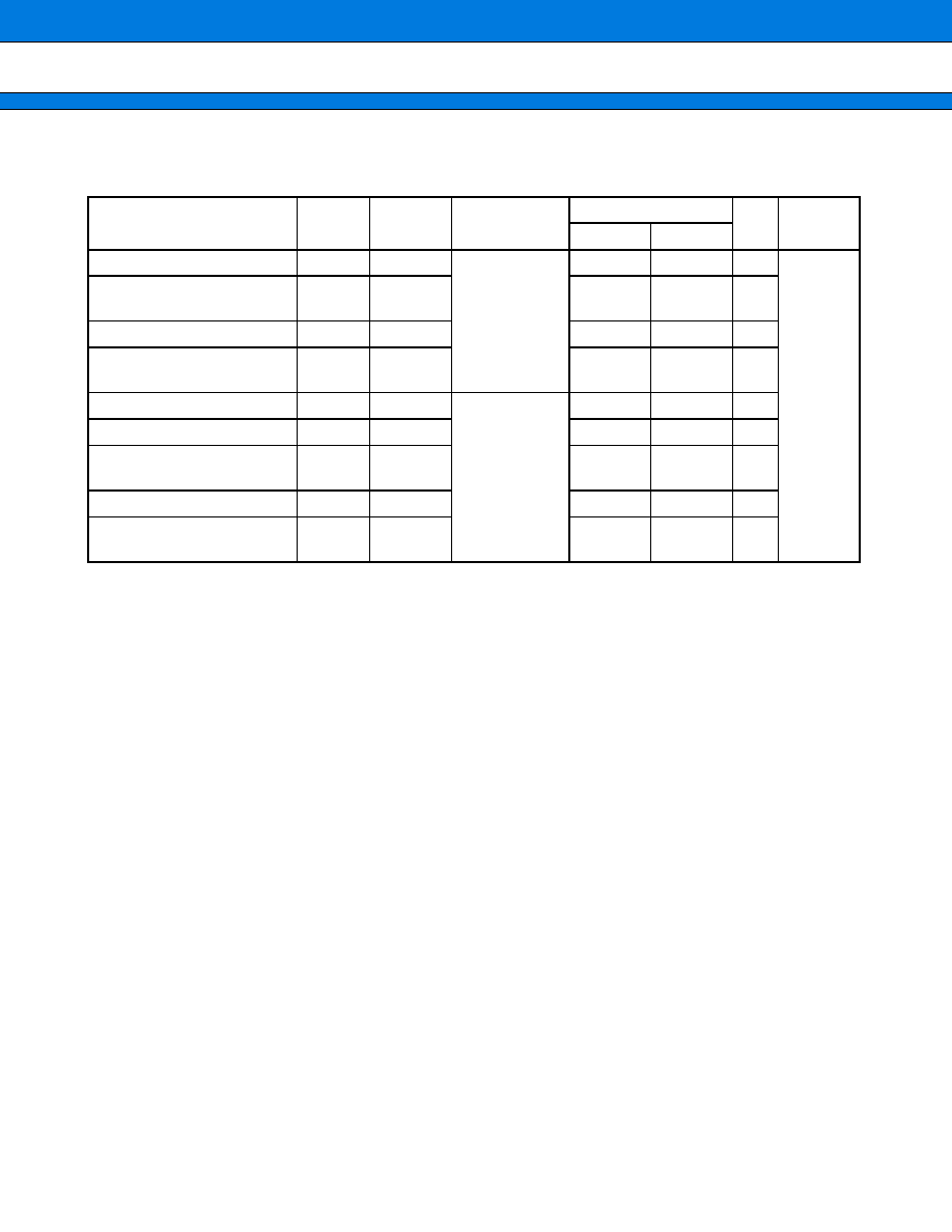
MB91110 Series
87
(14) UART Timing
(V
CC
5
=
5 V
±
10
%
, V
CC
3
=
3.3 V
±
5
%
, V
SS
=
AV
SS
=
AVRL
=
0 V, T
A
=
0
°
C to
+
70
°
C)
Notes :
·
This is the AC standard in the case of CLK synchronous mode.
·
t
CYCP
is the cycle time of the peripheral system clock.
Parameter
Symbol Pin Name
Conditions
Value
Unit
Remarks
Min
Max
Serial clock cycle time
t
SCYC
Internal shift
clock mode
8 t
CYCP
ns
SCLK
SOUT
Delay time
t
SLOV
-
80
80
ns
Valid SIN
SCLK
t
IVSH
100
ns
SCLK
Valid
SIN holding lock
t
SHIX
60
ns
Serial clock "H" pulse width
t
SHSL
External shift
clock mode
4 t
CYCP
ns
Serial clock "L" pulse width
t
SLSH
4 t
CYCP
ns
SCLK
SOUT
Delay time
t
SLOV
150
ns
Valid SIN
SCLK
t
IVSH
60
ns
SCLK
Valid
SIN holding lock
t
SHIX
60
ns

MB91110 Series
88
· Internal shift clock mode
· External shift clock mode
SCLK
SOUT
SIN
t
SCYC
t
SLOV
t
IVSH
t
SHIX
V
OH
V
OL
V
OL
V
OH
V
OL
V
IH
V
IL
V
IH
V
IL
SCLK
SOUT
SIN
t
SLOV
t
SLSH
t
SHSL
t
IVSH
t
SHIX
V
OH
V
OL
V
IH
V
IH
V
IL
V
IL
V
IL
V
IH
V
IL
V
IH

MB91110 Series
89
(15) Trigger System Input Timing
(V
CC
5
=
5 V
±
10
%
, V
CC
3
=
3.3 V
±
5
%
, V
SS
=
AV
SS
=
AVRL
=
0 V, T
A
=
0
°
C to
+
70
°
C)
Note : t
CYCP
is the cycle time of the peripheral system clock.
Parameter
Sym-
bol
Pin Name
Condi-
tions
Value
Unit
Remarks
Min
Max
A/D initiation trigger input time
t
TRG
ATG
5 t
CYCP
ns
PPG initiation trigger input time
TRG0 to
TRG5
ns
ATG
TRG0
to TRG5
t
TRG
V
IL
V
IL

MB91110 Series
90
(16) DMA Controller Timing
(V
CC
5
=
5 V
±
10
%
, V
CC
3
=
3.3 V
±
5
%
, V
SS
=
AV
SS
=
AVRL
=
0 V, T
A
=
0
°
C to
+
70
°
C)
Parameter
Sym-
bol
Pin Name
Condi-
tions
Value
Unit
Remarks
Min
Max
DREQ input pulse
width
t
DRWH
DREQ0 to DREQ2
2 t
CYC
ns
DACK delay time
(Normal bus)
(Normal DRAM)
t
CLDL
CLK
DACK0 to DACK2
6
ns
t
CLDH
6
ns
EOP delay time
(Normal bus)
(Normal DRAM)
t
CLEL
CLK
DEOP0 to DEOP2
6
ns
t
CLEH
6
ns
DACK delay time
(Single DRAM)
(Hyper DRAM)
t
CHDL
CLK
DACK0 to DACK2
n
/
2
×
t
CYC
ns
t
CHDH
6
ns
EOP delay time
(Single DRAM)
(Hyper DRAM)
t
CHEL
CLK
DEOP0 to DEOP2
n
/
2
×
t
CYC
ns
t
CHEH
6
ns
CLK
DREQ0 to DREQ2
2.4 V
2.4 V
2.4 V
2.4 V
0.8 V
0.8 V
0.8 V
0.8 V
2.4 V
2.4 V
DACK0 to DACK2
DEOP0 to DEOP2
DACK0 to DACK2
DEOP0 to DEOP2
(Single DRAM)
(Hyper DRAM)
t
CYC
t
DRWH
t
CLDL
t
CLEL
t
CHDL
t
CHEL
t
CLDH
t
CLEH
t
CHDH

MB91110 Series
91
5.
A/D Converter Electrical Characteristics
(V
CC
5
=
5 V
±
10
%
, V
CC
3
=
AV
CC
=
AVRH
=
3.3 V
±
5
%
, V
SS
=
AV
SS
=
AVRL
=
0 V, T
A
=
0
°
C to
+
70
°
C)
*1 : In case of V
CC
3
=
AV
CC
=
3.3 V
±
5%, machine clock 25 MHz
*2 : This is the current in the case that the A/D converter is not activated and the CPU is stopped (in case of
V
CC
3
=
A
VCC
=
AVRH
=
3.465 V)
Notes :
·
As the AVRH becomes smaller, the tolerance becomes relatively larger.
·
Output impedance of external circuits other than analog input must be used under the following
condition.
Output impedance of external circuits < 7 k
If the output impedance of the external circuits is too high, the sampling time for the analog voltage may be
insufficient.
Parameter
Sym-
bol
Pin Name
Value
Unit
Min
Typ
Max
Resolution
10
10
BIT
Conversion error
±
3.0
LSB
Linearity error
±
2.5
LSB
Differential linearity error
±
1.9
LSB
Zero transition error
V
OT
AN0 to AN7
-
1.5
+
0.5
+
2.5
LSB
Full-scale transition error
V
FST
AN0 to AN7
AVRH
-
4.5
AVRH
-
1.5
AVRH
+
0.5
LSB
Conversion time
5.6*
1
µ
s
Analog port input current
I
AIN
AN0 to AN7
0.1
10
µ
A
Analog input voltage
V
AIN
AN0 to AN7
AV
SS
AVRH
V
Standard voltage
AVRH
AV
SS
AV
CC
V
Power supply current
I
A
AV
CC
4
mA
I
AH
5*
2
µ
A
Standard voltage current supplied
I
R
AVRH
110
µ
A
I
RH
5*
2
µ
A
Tolerance between channels
AN0 to AN7
4
LSB
R
ON1
: 5 k
R
ON2
: 620
R
ON3
: 620
R
ON4
: 620
C
0
: 2 pF
C
1
: 2 pF
R
ON1
R
ON2
R
ON3
R
ON4
C
0
C
1
Analog input
Sample holding circuit
Comparator
Note : Figures described above should be considered as standard.

MB91110 Series
92
Definition of A/D Converter Terms
· Resolution
Analog changes that can be identified by A/D converter
· Linearity error
Difference between the straight line linking the zero transition point (00 0000 0000
00 0000 0001) to the
full-scale transition point (11 1111 1110
11 1111 1111) and actual conversion characteristics.
· Differential linearity error
Difference compared to the ideal input voltage value required to change the output code 1LSB
3FF
3FE
3FD
004
003
002
001
AVRL
AVRH
{1 LSB
×
(N
-
1)
+
V
OT
}
V
NT
(Actual measured value)
V
OT
(Actual measured value)
Digital output
Actual conversion characteristics
Ideal characteristics
Analog input
Actual conversion
characteristics
V
FST
(Actual
measured value)
N
-
1
AVRL
AVRH
N
-
2
N
N
+
1
Actual conversion
characteristics
Actual conversion
characteristics
Ideal characteristics
V
NT
(Actual measured value)
V
(N
+
1)T
(Actual measured value)
Digital output
Analog input
Linearity error of digital output N
=
V
NT
-
{1 LSB
×
(N
-
1)
+
V
OT
}
1 LSB
[LSB]
Differential linearity error of digital output N
=
V (
N
+
1
)
T
-
V
NT
1 LSB
-
1
1 LSB
=
V
FST
-
V
OT
1022
[V]
1 LSB (Ideal value)
=
AVRH
-
AVRL
1024
[V]
V
OT
: Voltage with digital output transferred from (000)
H
to (001)
H
V
FST
: Voltage with digital output transferred from (3FE)
H
to (3FF)
H
V
NT
: Voltage with digital output transferred from (N
-
1)
H
to N
[LSB]
[Linearity error]
[Differential linearity error]

MB91110 Series
93
· Total error
This indicates the difference between the actual and theoretical values and includes zero transition, full-scale
transition and linearity error.
3FF
3FE
3FD
004
003
002
001
AVRL
AVRH
1.5 LSB
0.5 LSB
{1 LSB
×
(N
-
1)
+
0.5 LSB}
Digital output
Analog input
Actual conversion
characteristics
Actual conversion
characteristics
Ideal characteristics
V
NT
(Actual measured value)
Total tolerance of digital output N
=
V
NT
-
{1 LSB
×
(N
-
1)
+
0.5 LSB}
1 LSB
[LSB]
V
OT
(Ideal value)
=
AVRL
+
0.5 LSB [V]
V
FST
(Ideal value)
=
AVRH
-
1.5 LSB [V]
V
NT
: Voltage with digital output transferred from (N
-
1)
H
to N
[Total error]

MB91110 Series
94
s
s
s
s
EXAMPLE CHARACTERISTICS
3
4
4.5
5
5.5
6
7
300
250
200
150
100
50
0
V
CC
[V]
V
OL
[mV]
V
OL
I
OL
= 4.0 mA, T
A
= 25 °C
3
4
4.5
5
5.5
6
7
6
5.5
5
4.5
4
3.5
3
V
CC
[V]
V
OH
[V]
V
OH
I
OH
= - 4.0 mA, T
A
= 25 °C
1
10
100
100
90
80
70
60
50
0
Frequency
[MHz]
I
CC3
[mV]
I
CC3
40
30
20
10
3
100
50
0
V
CC
[V]
I
CC3
[mA]
I
CC3
3.5
3.5
4.5
6.5
35
30
25
20
0
V
CC
[V]
I
CC5
[mA]
I
CC5
40
15
10
5
5.5
4
5
6
1
10
100
40
35
30
25
20
15
0
Frequency
[MHz]
I
CC5
[mA]
I
CC5
10
5
4
5
6
0
V
CC
[V]
T
A
= 25 °C
125
100
75
50
25
V
CC
= 3.3 V, T
A
= 25 °C
f = 50.0 MHz, T
A
= 25 °C
V
CC
= 5.0 V, T
A
= 25 °C
f = 25.0 MHz, T
A
= 25 °C
Pull-up resistance
Resistor value (k
)

MB91110 Series
95
3
2
1
0
-1
-2
-3
V
CC
= 3.0 V, AV
CC
= 3.0 V, T
A
= 25
°C
CODE
3
2
1
0
-1
-2
-3
3
2
1
0
-1
-2
-3
CODE
CODE
00
1FF
00
1FF
00
1FF
V
CC
= 3.0 V, AV
CC
= 3.0 V, T
A
= 25
°C
V
CC
= 3.0 V, AV
CC
= 3.0 V, T
A
= 25
°C
MB91110 Total error
MB91110 Linearity error
MB91110 Differential linearity error
Linearity error [LSB]
Differential Linearity error [LSB]
Total error [LSB]

MB91110 Series
96
s
s
s
s
ORDERING INFORMATION
Part number
Package
Remarks
MB91110PMT2
144-pin plastic LQFP
(FPT-144P-M08)
MB91V110CR
PGA-299C-A01

MB91110 Series
97
s
s
s
s
PACKAGE DIMENSION
144-pin plastic LQFP
(FPT-144P-M08)
Dimensions in mm (inches) .
C
2000 FUJITSU LIMITED F144019S-c-2-4
Details of "A" part
0.25(.010)
(Stand off)
(.004±.004)
0.10±0.10
(.024±.006)
0.60±0.15
(.020±.008)
0.50±0.20
1.50
+0.20
0.10
+.008
.004
.059
0°~8°
0.50(.020)
"A"
0.08(.003)
0.145±0.055
(.006±.002)
LEAD No.
1
36
INDEX
37
72
73
108
109
144
0.22±0.05
(.009±.002)
M
0.08(.003)
20.00±0.10(.787±.004)SQ
22.00±0.20(.866±.008)SQ
(Mounting height)

MB91110 Series
FUJITSU LIMITED
All Rights Reserved.
The contents of this document are subject to change without notice.
Customers are advised to consult with FUJITSU sales
representatives before ordering.
The information and circuit diagrams in this document are
presented as examples of semiconductor device applications, and
are not intended to be incorporated in devices for actual use. Also,
FUJITSU is unable to assume responsibility for infringement of
any patent rights or other rights of third parties arising from the use
of this information or circuit diagrams.
The products described in this document are designed, developed
and manufactured as contemplated for general use, including
without limitation, ordinary industrial use, general office use,
personal use, and household use, but are not designed, developed
and manufactured as contemplated (1) for use accompanying fatal
risks or dangers that, unless extremely high safety is secured, could
have a serious effect to the public, and could lead directly to death,
personal injury, severe physical damage or other loss (i.e., nuclear
reaction control in nuclear facility, aircraft flight control, air traffic
control, mass transport control, medical life support system, missile
launch control in weapon system), or (2) for use requiring
extremely high reliability (i.e., submersible repeater and artificial
satellite).
Please note that Fujitsu will not be liable against you and/or any
third party for any claims or damages arising in connection with
above-mentioned uses of the products.
Any semiconductor devices have an inherent chance of failure. You
must protect against injury, damage or loss from such failures by
incorporating safety design measures into your facility and
equipment such as redundancy, fire protection, and prevention of
over-current levels and other abnormal operating conditions.
If any products described in this document represent goods or
technologies subject to certain restrictions on export under the
Foreign Exchange and Foreign Trade Law of Japan, the prior
authorization by Japanese government will be required for export
of those products from Japan.
F0204
©
FUJITSU LIMITED Printed in Japan