Äîêóìåíòàöèÿ è îïèñàíèÿ www.docs.chipfind.ru
DS04-28827-1E
FUJITSU SEMICONDUCTOR
DATA SHEET
ASSP For Screen Display Control
CMOS
On-Screen Display Controller
MB90098A
s
s
s
s
DESCRIPTION
The FUJITSU MB90098A on-screen display controller is designed for use with LCD monitors, operates at a
maximum dot clock frequency of 140 MHz, and provides demultiplexed output (2-pixel parallel output) .
The maximum display screen configuration is 32 characters
×
16 rows, with a maximum resolution of 24
×
32
dots per character making the MB90098A ideal for use with SVGA, XGA, SXGA etc. LCD displays.
A variety of display functions are enabled including sprite characters, background characters, graphics functions
etc.
s
s
s
s
FEATURES
(Continued)
s
s
s
s
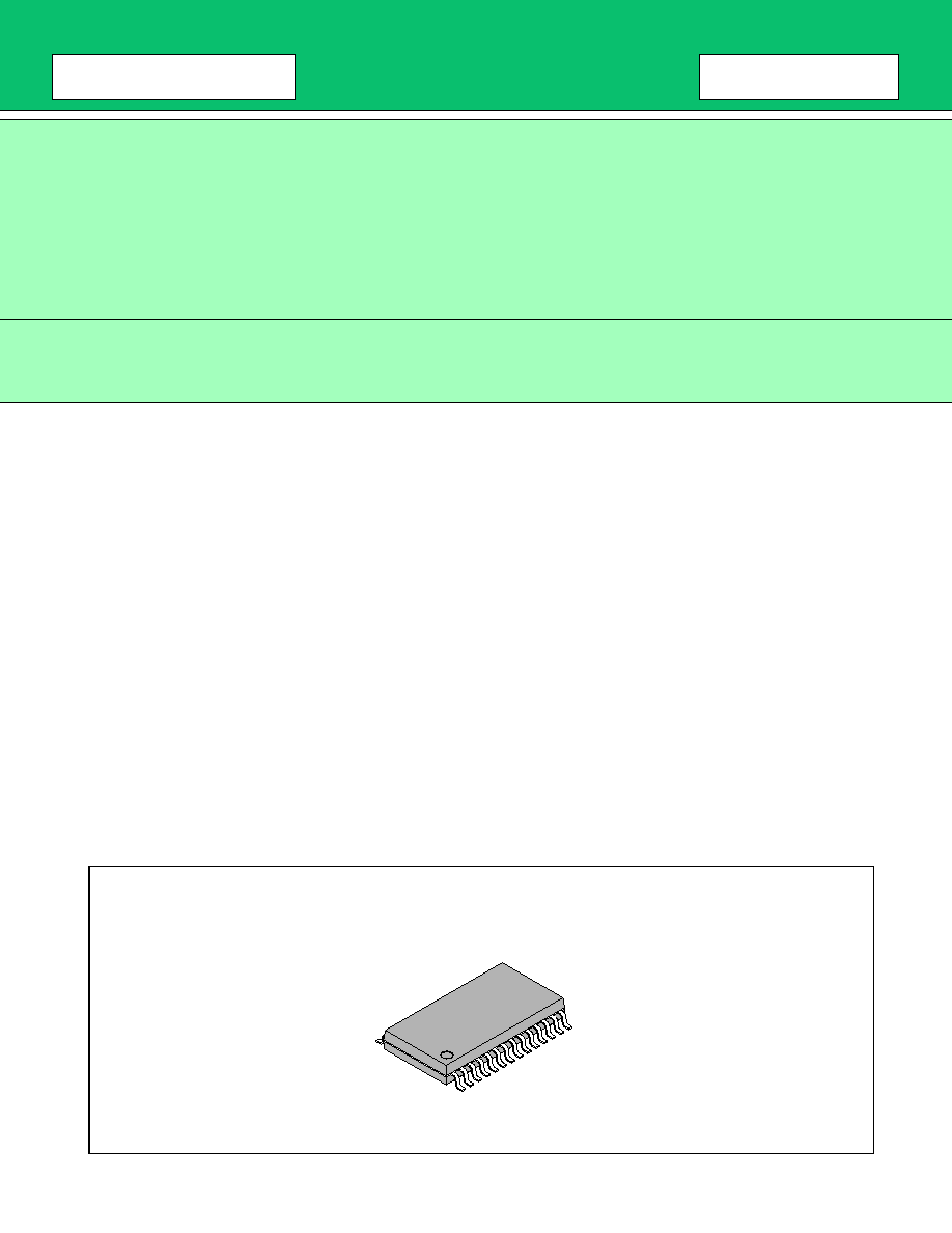
PACKAGE
· Main screen display capacity
Maximum 32 characters
×
16 rows
· Character configuration
L size : 24 dots (h)
×
2h* dots (v)
M size : 18 dots (h)
×
2h* dots (v)
S size : 12 dots (h)
×
2h* dots (v)
* : h
=
9 to 16
L, M, S sizes can be selected by character
h can be set to 2 values per screen
· Character type
512 character types built in
28-pin plastic SOP
(FPT-28P-M17)

MB90098A
2
(Continued)
· Display modes
Normal/graphic characters
(set for each character)
Border display (horizontal border
/pattern background)
(set for each screen)
Character background
(solid-fill/shaded)
(set for each character)
Row background (solid-fill/shaded)
(set for each row)
Enlarged (standard, double height,
double width, double height & width)
(set for each row)
Blinking : Select blinking character,
period, duty ratio
(set for each character)
(set for each screen)
· Sprite character display
(graphic display only)
Can display 1 block on main screen (Max. 2 characters wide
×
2 high) .
Only the first 256 characters can be used (code : 000
H
to 0FF
H
)
· Screen background character
display (graphic display only)
Repeated pattern below main screen (Max. 2 characters wide
×
2 high) .
Only the first 256 characters can be used (code : 000
H
to 0FF
H
)
· Display color
Character color/background color
Row background/character border color
Screen background color
Graphic character dot color
Shadow background border color
16 colors each (set for each character)
16 colors each (set for each row)
16 colors (set for each screen)
16 colors (set for each dot)
16 colors (set for each screen)
· Display position control
Horizontal display start position
Vertical display start position
Row spacing control
Control in 4-dot units (set for each
screen)
Control in 4-dot units (set for each
screen)
Control in 2-dot units (set for each
row)
· Character/color signal output Choice of straight output or demultiplexed output
DA3-DA0 (color signal) , VOBA (OSD display period output signal)
DB3-DB0 (color signal) , VOBB (OSD display period output signal)
· Clock frequency
140 MHz
· Microcontroller interface
16-bit serial input (3 signal input pins)
· Package
SOP-28
· Supply voltage
+
3.3 V
MB90098A
3
s
s
s
s
PIN ASSIGNMENT
(TOP VIEW)
(FPT-28P-M17)
1
2
3
4
5
6
7
8
9
10
11
12
13
14
DA0
DA1
DA2
DA3
VOBA
V
SS
DCLKO
V
DD
DB0
DB1
DB2
DB3
VOBB
BUSY
CS
SIN
SCLK
V
SS
DCLKI
V
SS
V
DD
TCLKI
V
DD
HSYNC
VSYNC
DISP
RESET
TEST
28
27
26
25
24
23
22
21
20
19
18
17
16
15
MB90098A
4
s
s
s
s
PIN DESCRIPTIONS
Pin
Pin no.
I/O
Circuit
type
Description
DCLKI
5
Input
B
Dot clock input pin
DCLKO
22
Output
A
Dot clock output pin
HSYNC
10
Input
B
Horizontal sync signal input pin. The active level is programmable.
VSYNC
11
Input
B
Vertical sync signal input pin. The active level is programmable.
DISP
12
Input
B
Display output control signal input pin. Input a high level signal to
enable display output. Input a low level signal to set the display
output (DA3-0, VOBA, DB3-0, VOBB pin output) to inactive level.
The active level is programmable.
DA3
DA2
DA1
DA0
25
26
27
28
Output
A
Color signal output pins. In straight output mode, the all-dot signal
is output. In demultiplexed output mode, the even dot signal is out-
put. The active level is programmable.
VOBA
24
Output
A
Display period signal output pin. In straight output mode, the all-
dot display period signal is output. In demultiplexed output mode,
the even dot display period signal is output. The active level is pro-
grammable.
DB3
DB2
DB1
DB0
17
18
19
20
Output
A
Color signal output pins. In demultiplexed output mode, the odd
dot signal is output. In straight output mode, the output is fixed at
inactive level. The active level is programmable.
VOBB
16
Output
A
Display period signal output pin. In demultiplexed output mode, the
odd dot display period signal is output. In straight output mode, the
output is fixed at inactive level. The active level is programmable.
BUSY
15
Output
A
Busy signal output pin. During internal VRAM fill operation, or in-
ternal command ROM transfer, a high level signal is output.
CS
1
Input
C
Chip select pin. During serial instruction transfer, a low level signal
is input.
SIN
2
Input
C
Serial data input pin.
SCLK
3
Input
C
Shift clock input pin for serial transfer.
RESET
13
Input
C
Reset signal input pin. Input a low level signal at power-on.
TEST
14
Input
C
Test signal input pin. Input a (fixed) high level signal during normal
operation.
V
DD
7, 9, 21
+
3.3 V power supply pins.
V
SS
4, 6, 23
Ground pins
TCLKI
8
Input
B
Test clock input pin. Input a (fixed) low level signal during normal
operation.

MB90098A
5
s
s
s
s
INPUT/OUTPUT CIRCUIT TYPES
Type
Circuit diagram
Remarks
A
· CMOS output
B
· CMOS hysteresis input
C
· CMOS hysteresis input with pull-up
resistance (approx. 50 k
)
Pch
Nch
MB90098A
6
s
s
s
s
BLOCK DIAGRAM
DA0
DA1
DA2
DA3
VOBA
DCLKO
DB0
DB1
DB2
DB3
VOBB
CS
SIN
SCLK
DCLKI
BUSY
HSYNC
VSYNC
DISP
RESET
(16 Kbyte)
Clock
Dot clock control
Command
ROM
transfer
control
Display
memory VRAM
(32 ch.
×
16 row)
Font
ROM
(512 fonts)
Command
ROM
Serial
input
control
Display control
EVEN
display
output
control
ODD
display
output
control

MB90098A
7
s
s
s
s
ABSOLUTE MAXIMUM RATINGS
(V
SS
=
0 V Typ.)
WARNING: Semiconductor devices can be permanently damaged by application of stress (voltage, current,
temperature, etc.) in excess of absolute maximum ratings. Do not exceed these ratings.
s
s
s
s
RECOMMENDED OPERATING CONDITIONS
(V
SS
=
0 V Typ.)
WARNING: The recommended operating conditions are required in order to ensure the normal operation of the
semiconductor device. All of the device's electrical characteristics are warranted when the device is
operated within these ranges.
Always use semiconductor devices within their recommended operating condition ranges. Operation
outside these ranges may adversely affect reliability and could result in device failure.
No warranty is made with respect to uses, operating conditions, or combinations not represented on
the data sheet. Users considering application outside the listed conditions are advised to contact their
FUJITSU representatives beforehand.
Parameter
Symbol
Rating
Unit
Remarks
Min.
Max.
Power supply voltage
V
DD
V
SS
-
0.5
V
SS
+
4.0
V
Input voltage
V
IN
V
SS
-
0.5
V
DD
+
0.5
V
Output voltage
V
OUT
V
SS
-
0.5
V
DD
+
0.5
V
Power consumption
Pd
400
mW
Operating temperature
Ta
0
70
°
C
Storage temperature
Tstg
-
55
+
125
°
C
Parameter
Symbol
Values
Unit
Remarks
Min.
Max.
Power supply voltage
V
DD
3.0
3.6
V
"H" level input voltage
V
IH
0.8
×
V
DD
V
DD
+
0.3
V
"L" level input voltage
V
IL
V
SS
-
0.3
0.2
×
V
DD
V
Operating temperature
Ta
0
70
°
C
MB90098A
8
s
s
s
s
ELECTRICAL CHARACTERISTICS
1.
DC Characteristics
(V
SS
=
0 V, Ta
=
0 to 70
°
C)
2.
Input/Output Pin Capacitance
Parameter
Symbol
Pin
Conditions
Values
Unit
Min.
Typ.
Max.
"H" level
output voltage
V
OH
All output
pins
V
DD
=
3.3 V
I
OH
=
-
8.0 mA
V
DD
-
0.5
V
"L" level
output voltage
V
OL
All output
pins
V
DD
=
3.3 V
I
OL
=
8.0 mA
0.4
V
Pull-up resistance
R
P
CS, SIN,
SCLK,
RESET,
TEST
V
DD
=
3.3 V
25
50
200
k
Input leak current
I
IL
DCLKI
HSYNC
VSYNC
DISP
V
I
=
0 V to V
DD
-
0.5
5.0
µ
A
Power supply current
I
DD
V
DD
V
DD
=
3.6 V
Dot clock 140 MHz
95
mA
V
DD
=
3.6 V
Dot clock 100 MHz
70
mA
V
DD
=
3.6 V
Dot clock 60 MHz
45
mA
V
DD
=
3.6 V
Dot clock 10 MHz
15
mA
Parameter
Symbol
Measurement conditions
Values
Unit
Min.
Max.
Input pins
C
IN
V
I
=
0 V, V
DD
=
0 V
f
=
1 MHz, Ta
=
25
°
C
16
pF
Output pins
C
OUT
16
pF
MB90098A
9
3.
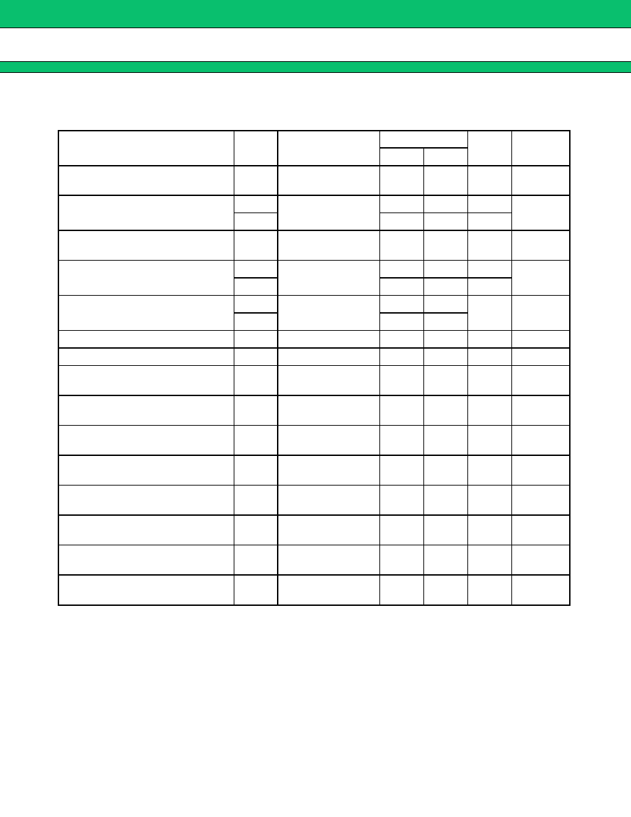
AC Characteristics
AC characteristics are measured under the following conditions :
Measurement conditions : C
=
28 pF, t
r
=
1 ns , t
f
=
1 ns, V
OH
=
0.8 V
DD
, V
OL
=
0.2 V
DD
, V
IH
=
0.8 V
DD
, V
IL
=
0.2 V
DD
(1) Serial Input Timing
(V
DD
=
3.3 V
±
0.3 V, V
SS
=
0 V, Ta
=
0 to 70
°
C)
Parameter
Symbol
Pin
Values
Unit
Remarks
Min.
Max.
Shift clock cycle time
t
CYC
SCLK
250
ns
Shift clock pulse width
t
WCH
SCLK
100
ns
t
WCL
100
ns
Shift clock signal rise-fall time
t
CR
SCLK
200
ns
t
CF
200
ns
Shift clock start time
t
SS
SCLK
100
ns
Data setup time
t
SU
SIN
100
ns
Data hold time
t
H
SIN
50
ns
Chip select end time
t
EC
CS
100
ns
Chip select signal rise-fall time
t
CRC
CS
200
ns
t
CFC
200
ns
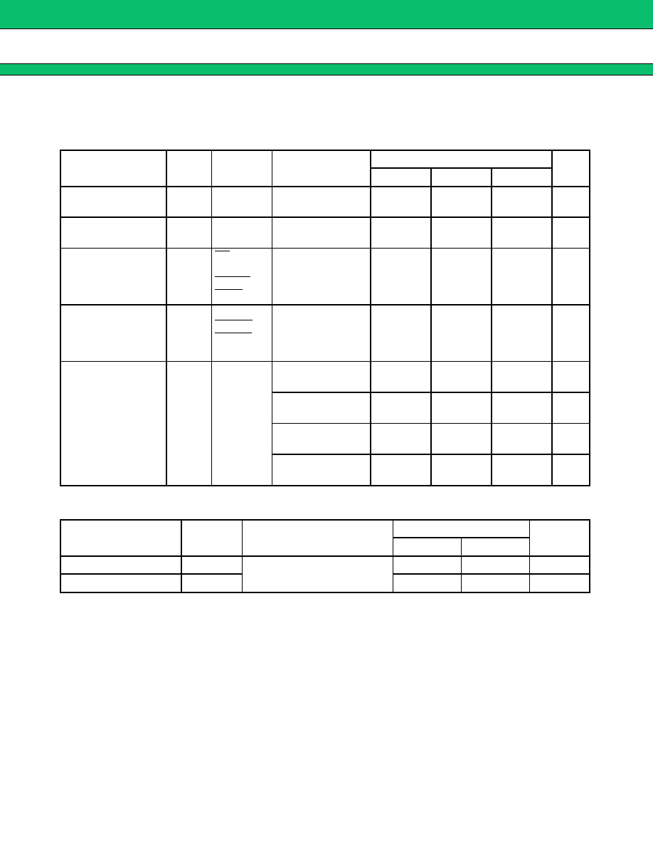
· Serial input timing
0.8 V
DD
0.2 V
DD
t
CRC
0.8 V
DD
0.2 V
DD
t
CFC
CS
t
CR
t
CF
0.8 V
DD
0.2 V
DD
t
EC
SCLK
0.8 V
DD
0.2 V
DD
SIN
t
SS
t
H
t
CYC
t
WCL
t
WCH
t
SU
MB90098A
10
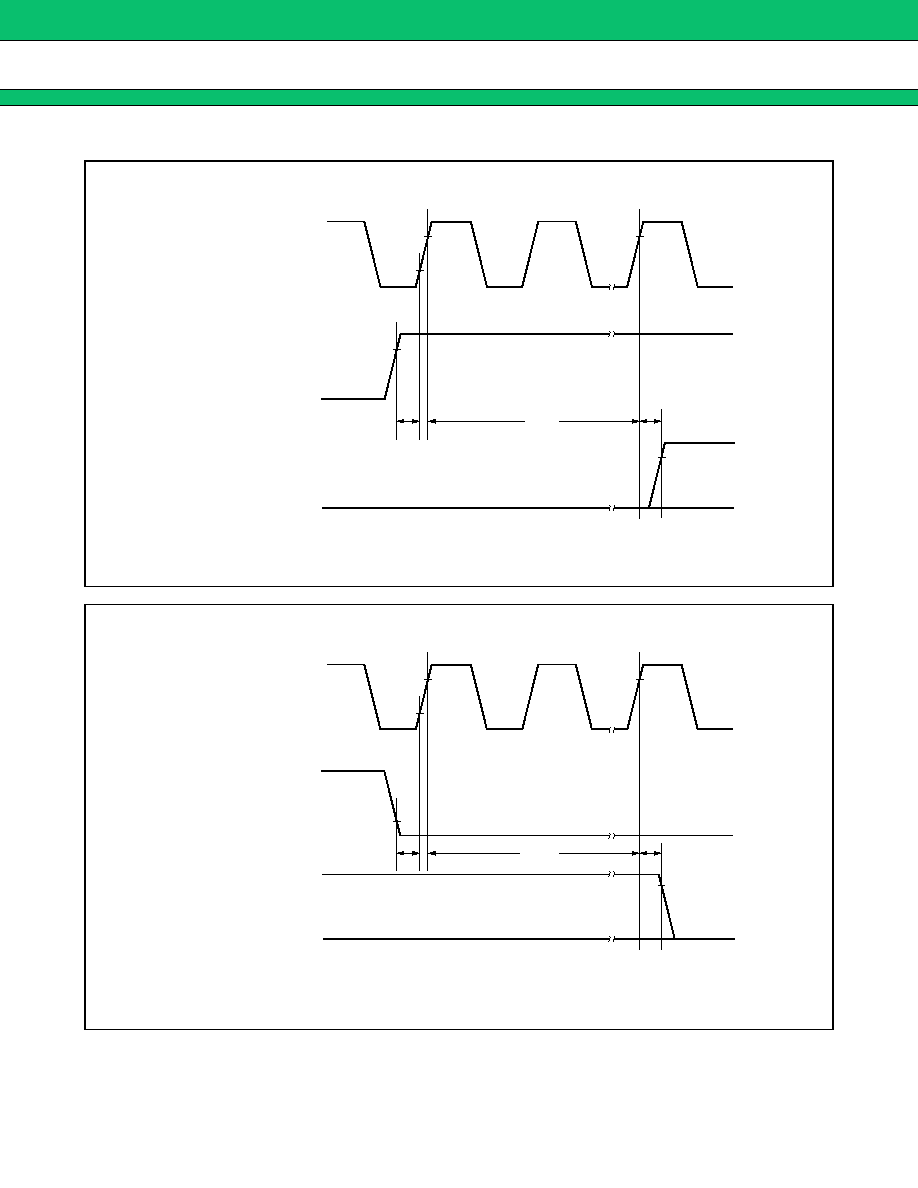
(2) Vertical Synchronization, Horizontal Synchronization, Display Output Control Signal Input Timing
(V
DD
=
3.3 V
±
0.3 V, V
SS
=
0 V, Ta
=
0 to 70
°
C)
* : During the horizontal synchronization pulse width, the MB90098A internal operations are temporarily paused
and writing to the internal VRAM is disabled. For this reason it is necessary to set both the horizontal synchro-
nization signal pulse width and the VRAM write cycle so that :
Horizontal sync signal pulse width < VRAM write cycle
Specifically, the period between instructions should be adjusted so that instruction 2 or instruction 4 (the VRAM
write instruction) is not repeated during the period of one horizontal sync signal pulse width.
If the above condition is not satisfied, writing to VRAM will not be executed normally.
Parameter
Symbol
Pin
Values
Unit
Remarks
Min.
Max.
Horizontal sync signal cycle time
t
HCYC
HSYNC
100
+
t
WH
Dot clock
Horizontal sync signal pulse width
t
WH
HSYNC
20
Dot clock
*
6
µ
s
Horizontal sync signal setup time
t
DHST
HSYNC
4
ns
Horizontal sync signal hold time
t
DHHD
0
ns
Vertical sync signal setup time
t
HVST
VSYNC
5
1H
-
5
Dot clock
Vertical sync signal hold time
t
HVHD
3
H
Display output control signal setup time
t
DDST
DISP
4
ns
Display output control signal hold time
t
DDHD
0
ns
Input sync signal rise-fall time
t
DR
t
DF
HSYNC
VSYNC
DISP
2
ns
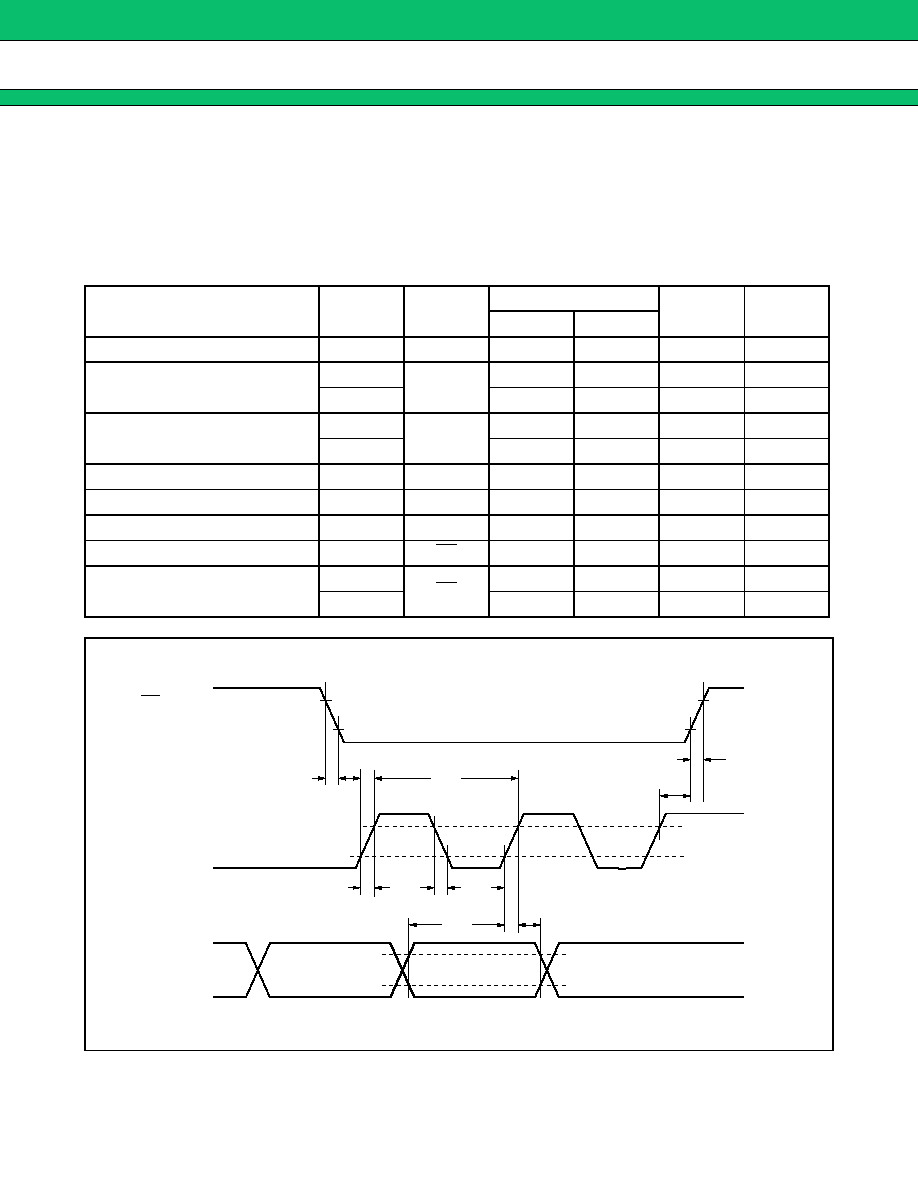
· Horizontal synchronization signal, display output control signal input timing
DCLKI
DISP
0.8 V
DD
0.2 V
DD
0.8 V
DD
0.2 V
DD
0.2 V
DD
t
DR
, t
DF
HSYNC
0.8 V
DD
0.2 V
DD
0.8 V
DD
0.2 V
DD
t
DR
, t
DF
0.8 V
DD
t
DHST
t
DHHD
t
DDST
t
DDHD
MB90098A
11
· Horizontal synchronization signal input
· Vertical synchronization signal input timing
VSYNC detection at HSYNC leading-edge
VSYNC detection at HSYNC trailing edge
t
WH
t
DF
t
DR
0.8 V
DD
0.2 V
DD
0.8 V
DD
0.8 V
DD
0.2 V
DD
HSYNC
t
HCYC
t
WH
t
DF
t
DR
0.8 V
DD
0.2 V
DD
0.8 V
DD
0.2 V
DD
t
DF
t
DR
0.8 V
DD
0.2 V
DD
0.8 V
DD
0.2 V
DD
HSYNC
VSYNC
t
HVHD
t
HVST
t
WH
t
DF
t
DR
0.8 V
DD
0.2 V
DD
0.8 V
DD
0.2 V
DD
t
DF
t
DR
0.8 V
DD
0.2 V
DD
0.8 V
DD
0.2 V
DD
HSYNC
VSYNC
t
HVHD
t
HVST
MB90098A
12
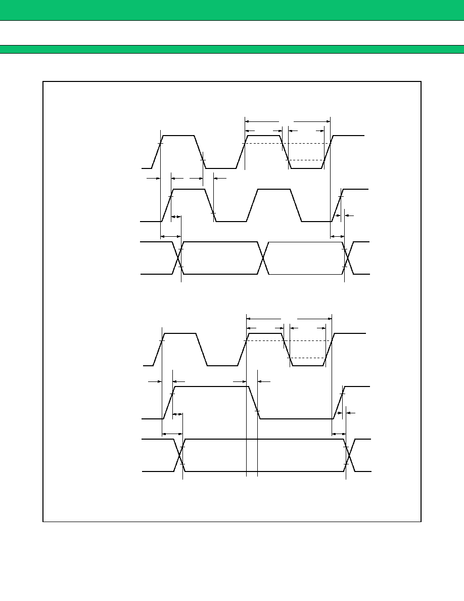
(3) Display Signal Timing
(V
DD
=
3.3 V
±
0.3 V, V
SS
=
0 V, Ta
=
0 to 70
°
C)
*1 : The maximum output frequency for straight output is 90 MHz.
*2 : The maximum output frequency for demultiplexed output is 70 MHz.
*3 : Use a continuous dot clock input signal without interruptions.
*4 : Actual display output varies according to control content, including display output control for each display layer,
display position control, etc.
Parameter
Symbol
Pin
Values
Unit
Remarks
Min.
Max.
Dot clock input cycle time
(straight output)
t
DIFS
DCLKI
10
90
MHz
* 1
* 3
Dot clock input pulse width
(straight output)
t
DIWHS
DCLKI
5
ns
* 1
* 3
t
DIWLS
5
ns
Dot clock input cycle time
(demultiplexed output)
t
DIFD
DCLKI
10
140
MHz
* 2
* 3
Dot clock input pulse width
(demultiplexed output)
t
DIWHD
DCLKI
3
ns
* 2
* 3
t
DIWLD
3
ns
Display output control on/off delay
time
t
DON
DA3 to DA0, VOBA
DB3 to DB0, VOBB
6
Dot
clock
*4
t
DOFF
6
Dot clock output delay time 1
t
PDCS
DCLKO
3
6
ns
*1
Dot clock output delay time 2
t
PDCD
DCLKO
3
7
ns
*2
Display signal output delay time I1
(straight output)
t
PDIS1
DA3 to DA0, VOBA
DB3 to DB0, VOBB
2
7
ns
*1
Display signal output delay time I2
(straight output)
t
PDIS2
DA3 to DA0, VOBA
DB3 to DB0, VOBB
1
6
ns
*1
Display signal output delay time O1
(straight output)
t
PDOS1
DA3 to DA0, VOBA
DB3 to DB0, VOBB
-
4
5
ns
*1
Display signal output delay time O2
(straight output)
t
PDOS2
DA3 to DA0, VOBA
DB3 to DB0, VOBB
-
5
4
ns
*1
Display signal output delay time I1
(demultiplexed output)
t
PDID1
DA3 to DA0, VOBA
DB3 to DB0, VOBB
2
7
ns
*2
Display signal output delay time I2
(demultiplexed output)
t
PDID2
DA3 to DA0, VOBA
DB3 to DB0, VOBB
1
6
ns
*2
Display signal output delay time O1
(demultiplexed output)
t
PDOD1
DA3 to DA0, VOBA
DB3 to DB0, VOBB
-
5
5
ns
*2
Display signal output delay time O2
(demultiplexed output)
t
PDOD2
DA3 to DA0, VOBA
DB3 to DB0, VOBB
-
6
4
ns
*2
MB90098A
13
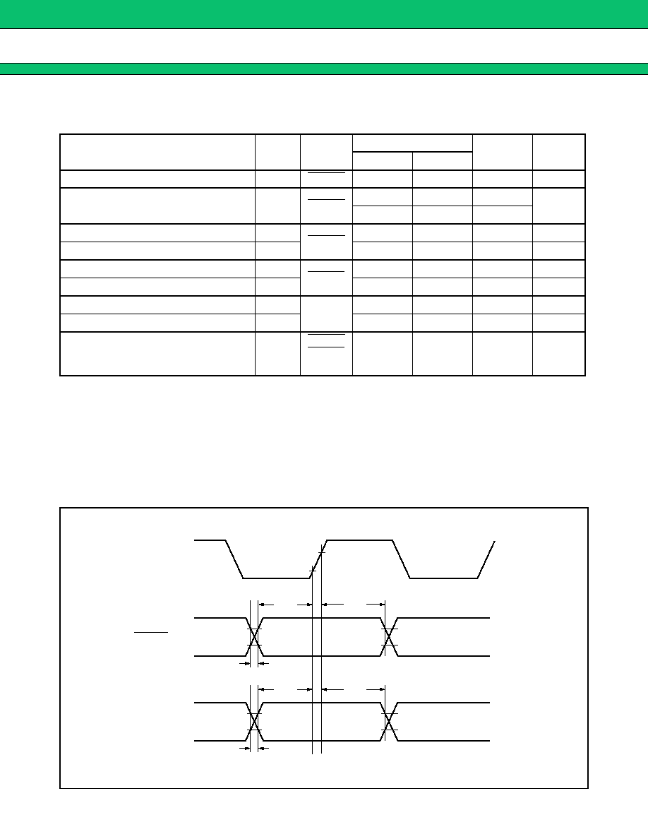
· Display output control ON timing
* : t
PDIXX
represents t
PDIS1
, t
PDIS2
, t
PDID1
, or t
PDID2
depending on the operating mode.
0.8 V
DD
0.8 V
DD
0.2 V
DD
0.8 V
DD
t
DON
t
DDST
t
PDIXX
*
DCLKI
DISP
DA3 to DA0
VOBA
DB3 to DB0
VOBB
· Display output control OFF timing
* : t
PDIXX
represents t
PDIS1
, t
PDIS2
, t
PDID1
, or t
PDID2
depending on the operating mode.
0.8 V
DD
0.2 V
DD
0.2 V
DD
0.8 V
DD
t
DOFF
t
DDST
t
PDIXX
*
DCLKI
DISP
DA3 to DA0
VOBA
DB3 to DB0
VOBB
MB90098A
14
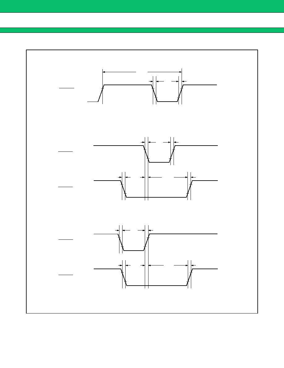
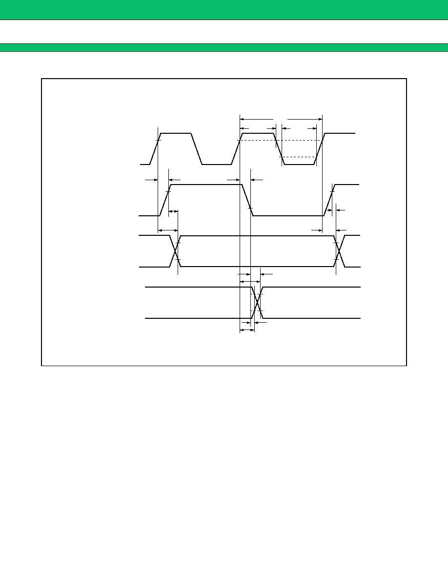
· Display signal output timing
Straight output
Demultiplexed output (single phase mode)
t
DIWLD
t
DIWHS
t
PDCS
t
PDOS1
t
PDIS1
t
PDOS2
t
PDIS2
t
PDCS
0.8 V
DD
0.2 V
DD
0.8 V
DD
0.2 V
DD
0.8 V
DD
0.8 V
DD
0.2 V
DD
0.8 V
DD
0.2 V
DD
0.8 V
DD
0.2 V
DD
DCLKI
DCLKO
DA3 to DA0
VOBA
DB3 to DB0
VOBB
t
DIFS
t
DIWLD
t
DIWHD
t
PDCD
t
PDOD1
t
PDID1
t
PDOD2
t
PDID2
t
PDCD
0.8 V
DD
0.2 V
DD
0.8 V
DD
0.8 V
DD
0.8 V
DD
0.2 V
DD
0.8 V
DD
0.2 V
DD
0.8 V
DD
0.2 V
DD
DCLKI
DCLKO
DA3 to DA0
VOBA
DB3 to DB0
VOBB
t
DIFD
MB90098A
15
· Display signal output timing
Demultiplexed output (2 phase mode)
t
DIWLD
t
DIWHD
t
PDCD
t
PDOD1
t
PDID1
t
PDOD1
t
PDID1
t
PDOD2
t
PDID2
t
PDOD2
t
PDID2
t
PDCD
0.8 V
DD
0.2 V
DD
0.8 V
DD
0.8 V
DD
0.8 V
DD
0.2 V
DD
0.8 V
DD
0.2 V
DD
0.8 V
DD
0.2 V
DD
0.8 V
DD
0.2 V
DD
t
DIFD
DCLKI
DCLKO
DA3 to DA0
VOBA
DB3 to DB0
VOBB

MB90098A
16
(4) Reset Input Timing
(V
DD
=
3.3 V
±
0.3 V, V
SS
=
0 V, Ta
=
0 to 70
°
C)
Parameter
Symbol
Pin
Values
Unit
Remarks
Min.
Max.
Reset pulse width
t
WRST
RESET
1
µ
s
Clock input
t
WRSD
DCLKI
5
Dot clock
· Reset input timing
RESET
DCLKI
0.2 V
DD
t
WRST
t
WRSD
MB90098A
17
s
s
s
s
DISPLAY CONTROL COMMANDS
1.
Command List
(Continued)
Com-
mand
No.
Function
Command Code/Data
15-12
11
10
9
8
7
6
5
4
3
2
1
0
0
VRAM write
address setting
0000 AY3
AY2
AY1
AY0
FL
0
0
AX4
AX3
AX2
AX1
AX0
1
Character data 1
setting
0001 MS1 MS0 MM1 MM0 MB3 MB2 MB1 MB0 MC3 MC2 MC1 MC0
2
Character data 2
setting
0010
MR
MG
MBL
M8
M7
M6
M5
M4
M3
M2
M1
M0
3
Row control data 1
setting
0011 LHS LW2 LW1 LW0 LFD
LFC
LFB
LFA
LF3
LF2
LF1
LF0
4
Row control data 2
setting
0100 LDS
0
LG1
LG0
LD
LE
LM1 LM0
L3
L2
L1
L0
5-00
Screen output
control 1A
0101
0
0
0
0
SDS UDS PDS DSP
0
0
0
0
5-03
Screen output
control 1B
0101
0
0
1
1
0
0
0
0
EOD EOT EOP EOO
5-1
Screen output
control 2
0101
0
1
FM1 FM0 BT1
BT0
BD1 BD0
0
0
0
0
5-2
Vertical display
position control
0101
1
0
0
Y8
Y7
Y6
Y5
Y4
Y3
Y2
Y1
Y0
5-3
Horizontal display
position control
0101
1
1
0
X8
X7
X6
X5
X4
X3
X2
X1
X0
6-0
Character vertical
size control
0110
0
0
0
0
0
HB2 HB1 HB0
0
HA2 HA1 HA0
6-1
Shaded background
frame color control
0110
0
1
0
0
BH3 BH2 BH1 BH0
BS3 BS2
BS1
BS0
6-2
Transparent color
control
0110
1
0
TC
0
TC3 TC2 TC1
TC0
0
0
0
0
6-3
Graphic color
control
0110
1
1
GF
GC
GF3 GF2 GF1 GF0 GC3 GC2 GC1 GC0
7-1
Screen background
character control 1
0111
0
1
PD1 PD0 PM7 PM6 PM5 PM4 PM3 PM2 PM1 PM0
7-3
Screen background
character control 2
0111
1
1
1
0
0
PH2 PH1 PH0
U3
U2
U1
U0
8-1
Sprite character
control 1
1000
0
1
SD1 SD0 SM7 SM6 SM5 SM4 SM3 SM2 SM1 SM0
8-2
Sprite character
control 2
1000
1
0
1
SBL
0
SH2 SH1 SH0
0
0
0
0

MB90098A
18
(Continued)
Note : When a reset signal is input (L level signal input to the RESET pin) , the screen output control 1A bits SDS,
UDS, PDS, DSP and the input/output pin control 1 bits DBX and DCX are initialized to "0." Other register
bits and VRAM contents are undefined.
After reset input/release is completed, set all register bits except for the command ROM transfer address
settings (commands 14-0, 14-1, 14-2, 14-3) and set all VRAM settings (character data and row control data) .
Com-
mand
No.
Function
Command Code/Data
15-12
11
10
9
8
7
6
5
4
3
2
1
0
9-0
Sprite character
control 3
1001
0
0
SY9
SY8
SY7
SY6
SY5
SY4
SY3
SY2
SY1
SY0
9-1
Sprite character
control 4
1001
1
0
SX9
SX8
SX7
SX6
SX5
SX4
SX3
SX2
SX1
SX0
11-0
Synchronization
control
1011
0
0
0
0
EG1
1
0
0
0
0
0
0
11-2 Dot clock control 1
1011
1
0
DO
0
0
0
0
0
0
0
0
0
13-0
Input/output pin
control 1
1101
0
0
0
VHE
HE
0
0
0
0
0
DBX DCX
13-1
Input/output pin
control 2
1101
0
1
0
0
0
0
0
0
0
IHX
IVX
IDX
14-0
CROM transfer start
address 1
1110
0
0
0
0
0
0
TSD TSC TSB TSA
TS9
TS8
14-1
CROM transfer start
address 2
1110
0
0
1
0
TS7
TS6
TS5
TS4
TS3
TS2
TS1
0
14-2
CROM transfer end
address 1
1110
0
1
0
0
0
0
TED TEC TEB TEA
TE9
TE8
14-3
CROM transfer end
address 2
1110
0
1
1
TSV
TE7
TE6
TE5
TE4
TE3
TE2
TE1
1

MB90098A
19
2.
Command Descriptions
· Command 0 (VRAM write address setting)
AY3-AY0 : Row address (0
H
-F
H
)
AX4-AX0 : Column address (0
H
-1F
H
)
FL : VRAM fill (0 : Off, 1 : On)
[Function]
This command sets the VRAM write address and turns VRAM fill on or off.
It is used to make row/column address settings before setting character data (issuing commands 1, 2) or to
make row address settings before setting line control data (issuing commands 3, 4) .
VRAM fill is activated by executing the character data setting 2 (command 2) .
[Additional information]
· For normal write operation (writing 1 character data or 1 row control data) the VRAM fill setting should be "Off"
(FL
=
0) .
· VRAM write address settings entered using this command are automatically incremented after each execution
of the character data setting 2 command (command 2) . (After the last column the address increment is to the
first column of the next row, and after the last column of the last row the address increment is to the first column
of the first row.)
· The VRAM fill function is a function that sets the same character data specified by the character data command
setting 1, 2 (command 1, 2) to character VRAM starting from the row and column address specified by command
0 to the final row (row 16) and final column (column 32) . The VRAM fill function is activated by the execution
of the character data setting 2 command (command 2) .
· During activation and execution of VRAM fill, the BUSY pin outputs an H level signal.
· During VRAM fill execution, do not issue commands 1-4.
(Caution)
· During row control data setting (command 3, 4) the column address (AX4-AX0) is ignored. Also, the address
is not incremented automatically after row control data setting.
· The VRAM fill setting is effective only during character data setting (command 1, 2) .
15
14
13
12
11
10
9
8
7
6
5
4
3
2
1
0
0
0
0
0
AY3
AY2
AY1
AY0
FL
0
0
AX4
AX3
AX2
AX1
AX0

MB90098A
20
· Command 1 (Character data 1 setting)
MC3-MC0 : Character color (16 colors)
MB3-MB0 : Background color (16 colors)
MM1, MM0 : Character background control
(0, 0 : Off)
(0, 1 : Solid fill)
(1, 0 : concaved shaded)
(1, 1 : convexed shaded)
MS1, MS0 : Character horizontal size control
(0, 0 : 12 dots)
(0, 1 : 18 dots)
(1, 0 : 24 dots)
(1, 1 : Setting prohibited)
[Function]
This command sets character data. Settings are entered in VRAM and reflected on the screen by executing the
character data setting 2 command (command 2) .
[Additional information]
· Character color, character background color, character background control and character horizontal size can
be set in any combination for each character separately.
· Shadow effects can be set for any combination of top, bottom, left, and right directions using the combination
of the character data setting 2 (command 2) MR bit and the row control data setting 2 (command 4) LD and
LE bits.
· Shadow background frame color settings are made by shaded background frame color control (command 6-1) .
15
14
13
12
11
10
9
8
7
6
5
4
3
2
1
0
0
0
0
1
MS1 MS0 MM1 MM0 MB3 MB2 MB1 MB0 MC3 MC2 MC1 MC0

MB90098A
21
· Command 2 (Character data setting 2)
MR : Shaded background succeeding character merge control
(0 : Not merged with succeeding character)
(1 : Merged with succeeding character)
M8-M0 : Character code
MG : Character/graphic character control
(0 : Character, 1 : Graphic character)
MBL : Blink control (0 : Off, 1 : On)
[Function]
This command writes the character data set by the character data setting 1 command (command 1) together
with the settings in this command, to VRAM at the address specified by the VRAM write address setting command
(command 0) .
After this command is executed, the VRAM write address is automatically incremented.
[Additional information]
· Setting the blink control bit to "On" (MBL
=
1) causes the display to blink according to the setting of the screen
output control 2 (command 5-1) BT1, BT0, BD1, BD0 bits.
· The shadow background right character combination control bit (MR) is used only with characters for which
the shadow background is specified by the character data setting 1 (command 1) bit (MM1
=
1) .
(Caution)
· At power-on, the contents of VRAM are undefined. Be sure to set all RAM data before the display is started.
15
14
13
12
11
10
9
8
7
6
5
4
3
2
1
0
0
0
1
0
MR
MG
MBL
M8
M7
M6
M5
M4
M3
M2
M1
M0

MB90098A
22
· Command 3 (Row control data setting 1)
LHS : Row character vertical size type control
(0 : Character vertical size A)
(1 : Character vertical size B)
LW2-LW0 : Row spacing control
(0-14 dots, in 2-dot units)
LF3-LF0 : Border color (16 colors)
LFD, LFC : Border output control
(0, 0 : All off)
(0, 1 : No character background, character only border on)
(1, 0 : No character background, solid fill character only border on)
(1, 1 : Border output on)
LFB, LFA : Border control
(0, 0 : Border off)
(0, 1 : Right border)
(1, 0 : Left border)
(1, 1 : Left, right border)
[Function]
This function sets row control data.
Settings are written to row VRAM and reflected on the screen when the row control data setting 2 command
(command 4) is executed.
[Additional information]
· The character vertical size A/B setting selected by the row character vertical size type control bit (LHS) applies
the character vertical size type control setting (command 6-0) .
· The border format setting applies the border format control setting (FM1, FM0) in the screen output control 2
command (command 5-1) .
15
14
13
12
11
10
9
8
7
6
5
4
3
2
1
0
0
0
1
1
LHS LW2 LW1 LW0 LFD
LFC
LFB
LFA
LF3
LF2
LF1
LF0

MB90098A
23
· Command 4 (Row control data setting 2)
LDS : Row character output control
(0 : Off, 1 : On)
LG1, LG0 : Row enlargement control
(0, 0 : Normal)
(0, 1 : Double width)
(1, 0 : Double height)
(1, 1 : Double height & width)
LE : Character background extention control
(0 : Normal, 1 : Extended)
LD : Shadow background lower row link control
(0 : Separate, 1 : Lower row link)
LM1, LM0 : Row background control
(0, 0 : Off)
(0, 1 : Solid display)
(1, 0 : Shadow concave)
(1, 1 : Shadow convex)
L3-L0 : Row background color (16 colors)
[Function]
This command writes the data set in the row control data setting 1 command (command 3) , together with the
settings in this command, to VRAM at the address specified by the set VRAM write address command (command
0) .
[Additional Information]
· The shadow background lower row link control bit (LD bit) applies to the character background shadow and
row background shadow effects.
(Caution)
· At power-on, the contents of VRAM are undefined. Be sure to set all RAM data before the display is started.
· After this command is executed, the VRAM write address is not automatically incremented. It is necessary to
set the VRAM write address (command 0) for each row for which row control data is set.
15
14
13
12
11
10
9
8
7
6
5
4
3
2
1
0
0
1
0
0
LDS
0
LG1
LG0
LD
LE
LM1 LM0
L3
L2
L1
L0
MB90098A
24
· Command 5-00 (Screen output control 1A)
SDS : Sprite character output control
(0 : Off, 1 : On)
UDS : Screen background output control
(0 : Off, 1 : On)
PDS : Screen background character output control
(0 : Off, 1 : On)
DSP : Display output control
(Character
+
border
+
character background
+
row background control)
(0 : Off, 1 : On)
[Function]
This command controls screen display output.
· Command 5-03 (Screen output control 1B)
EOD : Demultplexed output synchronization control
(0 : Internal HSYNC sychronization)
(1 : DISP synchronization)
EOT : Demultiplexed output timing control
(0 : Synchronized timing
+
0 clock)
(1 : Synchronized timing
+
1 clock)
EOP : Demultiplexed output phase control
(0 : Synchronized output)
(1 : 2-phase output)
EOO : Straight/demultiplexed output control
(0 : Straight output)
(1 : Demultiplexed output)
[Function]
This function controls screen display output.
[Additional information]
· By setting the straight/demultiplexed output selection to demultiplexed output (EOO
=
1) , the display signal is
output in parallel from the DA3-0, VOBA pins and the DB3-0, VOBB pins.
· When the demultiplexed output synchronization control selection is "Internal HSYNC synchronization" (EOD
=
0) , the horizontal sync operating edge selection is determined by the horizontal sync operating edge setting
(HE bit) in the input/output pin control 1 command (command 13-0) .
15
14
13
12
11
10
9
8
7
6
5
4
3
2
1
0
0
1
0
1
0
0
0
0
SDS UDS PDS DSP
0
0
0
0
15
14
13
12
11
10
9
8
7
6
5
4
3
2
1
0
0
1
0
1
0
0
1
1
0
0
0
0
EOD EOT EOP EOO
MB90098A
25
· Command 5-1 (Screen output control 2)
BT1, BT0 : Blink period control
(0, 0 : 16 V)
(0, 1 : 32 V)
(1, 0 : 48 V)
(1, 1 : 64 V)
BD1, BD0 : Blink duty control
(0, 0 : On : Off
=
1 : 0 always on)
(0, 1 : On : Off
=
1 : 1)
(1, 0 : On : Off
=
1 : 3)
(1, 1 : On : Off
=
3 : 1)
FM1, FM0 : Border format control
(0, 0 : Side border 1 dot)
(0, 1 : Side border 2 dot)
(1, 0 : Pattern background 1)
(1, 1 : Pattern background 2)
[Function]
This function controls screen display output.
[Additional Information]
· The blink period control and blink duty control settings apply to control of characters specified for blink control
(MBL
=
1) in the character data setting 2 command (command 2) as well as to sprite characters specified for
sprite character blink control (SBL
=
1) in the sprite character control 2 command (command 8-2) .
· Command 5-2 (Vertical display position control)
Y8-Y0 : Vertical display position control
(0-2044, 4-dot units)
[Function]
This function controls the vertical display position on the screen.
· Command 5-3 (Horizontal display position control)
X8-X0 : Horizontal display position control
(0-2044, 4-dot units)
[Function]
This function controls the horizontal display position on the screen.
15
14
13
12
11
10
9
8
7
6
5
4
3
2
1
0
0
1
0
1
0
1
FM1 FM0 BT1
BT0
BD1 BD0
0
0
0
0
15
14
13
12
11
10
9
8
7
6
5
4
3
2
1
0
0
1
0
1
1
0
0
Y8
Y7
Y6
Y5
Y4
Y3
Y2
Y1
Y0
15
14
13
12
11
10
9
8
7
6
5
4
3
2
1
0
0
1
0
1
1
1
0
X8
X7
X6
X5
X4
X3
X2
X1
X0
MB90098A
26
· Command 6-0 (Character vertical size control)
HB2-HB0 : Character vertical size control B
(18-32 dots, 2-dot units)
HA2-HA0 : Character vertical size control A
(18-32 dots, 2-dot units)
[Function]
This function controls the character vertical size A and B settings.
[Additional Information]
· The main screen display allows a selection between character sizes A and B by row. In the set row data 1
command (command 3) , the selection of character size A or B is made by the row character vertical size type
control (LHS bit) . This command is used to set the vertical display dot count of both type A and B.
· Command 6-1 (Shaded background frame color control)
BH3-BH0 : Shadow background frame highlight color (16 colors)
BS3-BS0 : Shadow background frame shadow color (16 colors)
[Function]
This function controls the shadow background border color.
[Additional Information]
· The shadow background border color is determined by the shadow character background designation (MM1
=
1) in the character data setting 1 command (command 1) , as well as the shadow row background designation
(LM1
=
1) in the row control data setting 2 command (command 4) .
· The shadow background border highlight color and shadow color are shown in the following areas :
· Command 6-2 (Transparent color control)
TC : Transparent color control
(0 : Off, 1 : On)
TC3-TC0 : Transparent color code (16 colors)
15
14
13
12
11
10
9
8
7
6
5
4
3
2
1
0
0
1
1
0
0
0
0
0
0
HB2 HB1 HB0
0
HA2 HA1 HA0
15
14
13
12
11
10
9
8
7
6
5
4
3
2
1
0
0
1
1
0
0
1
0
0
BH3 BH2 BH1 BH0 BS3
BS2
BS1
BS0
Character background
Row background
Shadow
background
concave
Shadow
background
convex
Shadow
background
concave
Shadow
background
convex
Shadow background
frame highlight color
Lower edge,
right edge
Upper edge,
left edge
Lower edge
Upper edge
Shadow background
frame shadow color
Upper edge,
left edge
Lower edge,
right edge
Upper edge
Lower edge
15
14
13
12
11
10
9
8
7
6
5
4
3
2
1
0
0
1
1
0
1
0
TC
0
TC3
TC2
TC1
TC0
0
0
0
0
MB90098A
27
[Function]
This function controls the transparent color.
[Additional Information]
· The transparent color code (TC3-TC0) may be set to any desired color code, and the transparent color control
set to On (TC
=
1) so that any display area of the specified color will be rendered invisible. Areas of the specified
color will be output as the underlying layer display.
· Command 6-3 (Graphic color control)
GF : Graphic color border color replacement control
(0 : Off, 1 : On)
GC : Graphic color character color replacement control
(0 : Off, 1 : On)
GF3-GF0 : Border color replacement color code (16 colors)
GC3-GC0 : Character color replacement color code (16 colors)
[Function]
This function replaces a specified color in graphic characters with a character color or border color in the display.
[Additional information]
· The graphic character display color is fixed and registered in font ROM. This command can be used to replace
any specified graphic character display color with the border color or character color.
· Any desired color in a graphic character (specified by the GF3-GF0 bits) can be replaced by the border color
(LF3-LF0) set in the row control data setting 1 command (command 3) .
· Any desired color in a graphic character (specified by the GC3-GC0 bits) can be replaced by the character
color (MC3-MC0) set in the character data setting 1 command (command 1) .
· If the graphic color border color replacement control is on (GF bit
=
1) and the transparent color control is on
(TC bit
=
1 in command 6-2) , and also the graphic color border color replacement color code is the same as
the transparent color code (TC3-0 in command 6-2) , the border color replacement has priority.
· If the graphic color border color replacement control is on (GF bit
=
1) and the transparent color control is on
(TC bit
=
1 in command 6-2) , and also the border color of the border color replacement color code (LF3-LF0
in command 3) is the same as the transparent color code (TC3-0 in command 6-2) , the color will be transparent
and the lower layer color will be displayed.
· If the graphic color character color replacement control is on (GC bit
=
1) and the transparent color control is
on (TC bit
=
1 in command 6-2) , and also the graphic color character color replacement color code is the
same as the transparent color code (TC3-0 in command 6-2) , the character color replacement has priority.
· If the graphic color character color replacement control is on (GC bit
=
1) and the transparent color control is
on (TC bit
=
1 in command 6-2) , and also the characterer color of the characterer color replacement color
code (MC3-MC0 in command 1) is the same as the transparent color code (TC3-0 in command 6-2) , the color
will be transparent the the lower layer color will be displayed.
· If the graphic color character color replacement control is on (GC bit
=
1) and the graphic color border color
replacement control is on (GF bit
=
1) , the character color replacement color code (GC3-GC0 bits) and border
color replacement color code (GF3-GF0 bits) should be set to different colors.
(Caution)
· This command applies only to the color of main screen graphic characters. It has no affect on the color of
sprite characters of screen background character dot colors.
15
14
13
12
11
10
9
8
7
6
5
4
3
2
1
0
0
1
1
0
1
1
GF
GC
GF3 GF2 GF1 GF0 GC3 GC2 GC1 GC0
MB90098A
28
· Command 7-1 (Screen background character control 1)
PD1, PD0 : Screen background character configuration control
(0, 0 : 1 character)
(0, 1 : 2 characters horizontal)
(1, 0 : 2 characters vertical)
(1, 1 : 2 characters horizontal
×
2 vertical)
PM7-PM0 : Screen background character code
(000
H
to 0FF
H
, 256 types)
[Function]
This function controls screen background characters.
[Additional Information]
· Screen background character control is applied when the screen background character output control bit is
turned On (PDS
=
1) in the screen output control 1A command (command 5-00) .
· The vertical size of screen background characters can be controlled by setting the screen background character
vertical size control bits (PH2-PH0) in the screen background character control 2 command (command 7-3) .
(Caution)
· Screen background characters can be displayed only as graphic characters.
· The screen background character code (PM7-PM0) can be set to only 256 code settings from 000h to 0FFh.
· The screen background character graphic color cannot be controlled by the graphic color control (command
6-3) graphic color border color replacement control or graphic color character color replacement control.
· Command 7-3 (Screen background character control 2)
PH2-PH0 : Screen background character vertical size control
(18-32 dots in 2-dot units)
U3-U0 : Screen background color (16 colors)
[Function]
This function controls screen background characters and screen background colors.
[Additional Information]
· The screen background color is displayed by setting the screen output control (command 5-00) screen back-
ground output control bit to on (UDS
=
1) .
· Screen background characters are displayed by setting the screen output control (command 5-00) screen
background character output control bit to on (PDS
=
1) .
15
14
13
12
11
10
9
8
7
6
5
4
3
2
1
0
0
1
1
1
0
1
PD1 PD0 PM7 PM6 PM5 PM4 PM3 PM2 PM1 PM0
15
14
13
12
11
10
9
8
7
6
5
4
3
2
1
0
0
1
1
1
1
1
1
0
0
PH2 PH1 PH0
U3
U2
U1
U0
MB90098A
29
· Command 8-1 (Sprite character control 1)
SD1, SD0 : Sprite character configuration control
(0, 0 : 1 character)
(0, 1 : 2 characters horizontal)
(1, 0 : 2 characters vertical)
(1, 1 : 2 characters horizontal
×
2 vertical)
SM7-SM0 : Sprite character code
(000
H
to 0FF
H
, 256 types)
[Function]
This function controls sprite characters.
[Additional Information]
· Sprite characters are displayed by setting the screen output control (command 5-00) sprite character output
control bit to on (SDS
=
1) . This will start sprite character display.
· The sprite character display position is determined by setting the sprite character control 3 command (command
9-0) and sprite character control 4 command (command 9-1) .
· The vertical size of the sprite character display is determined by the sprite character vertical size control bits
(SH2-SH0) in the sprite character control 2 command (command 8-2) .
· The sprite character blink control bit (SBL) turns sprite character blinking on and off.
· The sprite character blink period and duty are controlled by the settings of the BT1, BT0, BD1, BD0 bits in the
screen output control command (command 5-1) .
(Caution)
· Sprite characters can only be displayed as graphic characters.
· The sprite character code (PM7-PM0) can be set to only 256 code settings from 000h to 0FFh.
· The sprite character graphic color cannot be controlled by the graphic color control (command 6-3) graphic
color border color replacement control or graphic color character color replacement control.
· command 8-2 (Sprite character control 2)
SBL : Sprite character blink control
(0 : Off, 1 : On)
SH2-SH0 : Sprite character vertical size control
(18-32 dots, in 2-dot units)
[Function]
This function controls sprite characters.
[Additional Information]
· See the additional information under sprite character control 1 (command 8-1) .
15
14
13
12
11
10
9
8
7
6
5
4
3
2
1
0
1
0
0
0
0
1
SD1 SD0 SM7 SM6 SM5 SM4 SM3 SM2 SM1 SM0
15
14
13
12
11
10
9
8
7
6
5
4
3
2
1
0
1
0
0
0
1
0
1
SBL
0
SH2 SH1 SH0
0
0
0
0
MB90098A
30
· Command 9-0 (Sprite character control 3)
Y9-SY0 : Sprite character vertical display position control
(0-2046, 2-dot units)
[Function]
This function controls sprite characters.
[Additional Information]
· See the additional information under sprite character control 1 (command 8-1) .
· Command 9-1 (Sprite character control 4)
SX9-SX0 : Sprite character horizontal display position control
(0-2046, 2-dot units)
[Function]
This function controls sprite characters.
[Additional Information]
· See the additional information under sprite character control 1 (command 8-1) .
· Command 11-0 (Synchronization control)
EG1 : Vertical enlargement control
(0 : Normal, 1 : Double)
[Function]
This function controls vertical enlargement in the synchronization system.
[Additional information]
· The vertical enlargement control bit (EG1) adjusts the vertical display size by controlling the horizontal syn-
chronization count. This control affects the vertical size of the entire display, not only the display position.
· Command 11-2 (Dot Clock Control)
DO : Dot clock pin output control
(0 : Off, 1 : On)
[Function]
This function controls dot clock output.
[Additional information]
· The internal dot clock signal can be output from the DCLKO pin by setting the dot clock pin output control bit
to on (DO
=
1) .
15
14
13
12
11
10
9
8
7
6
5
4
3
2
1
0
1
0
0
1
0
0
SY9
SY8
SY7
SY6
SY5
SY4
SY3
SY2
SY1
SY0
15
14
13
12
11
10
9
8
7
6
5
4
3
2
1
0
1
0
0
1
1
0
SX9
SX8
SX7
SX6
SX5
SX4
SX3
SX2
SX1
SX0
15
14
13
12
11
10
9
8
7
6
5
4
3
2
1
0
1
0
1
1
0
0
0
0
EG1
1
0
0
0
0
0
0
15
14
13
12
11
10
9
8
7
6
5
4
3
2
1
0
1
0
1
1
1
0
DO
0
0
0
0
0
0
0
0
0

MB90098A
31
· Command 13-0 (Input/Output Pin Control 1)
VHE : HSYNC edge selection for vertical sync detection
(0 : Leading edge, 1 : Trailing edge)
HE : Edge selection for horizontal sync operation
(0 : Trailing edge, 1 : Leading edge)
DCX : Display color signal output logic control
(0 : Positive logic, 1 : Negative logic)
DBX : Display output period signal output logic control
(0 : Positive logic, 1 : Negative logic)
[Function]
This function controls the input/output pins.
[Additional Information]
· Vertical vibration phenomena can be avoided by adjusting the input phase timing of the vertical sync signal
and horizontal sync signal, using the VHE bit to select the HSYNC edge for vertical sync detection.
· Command 13-1 (Input/Output Pin Control 2)
IHX : Horizontal sync signal input logic control
(0 : Negative logic, 1 : Positive logic)
IVX : Vertical sync signal input logic control
(0 : Negative logic, 1 : Positive logic)
IDX : Display period signal logic control
(0 : Positive logic, 1 : Negative logic)
[Function]
This function controls the input pins.
15
14
13
12
11
10
9
8
7
6
5
4
3
2
1
0
1
1
0
1
0
0
0
VHE
HE
0
0
0
0
0
DBX DCX
15
14
13
12
11
10
9
8
7
6
5
4
3
2
1
0
1
1
0
1
0
1
0
0
0
0
0
0
0
IHX
IVX
IDX
MB90098A
32
· Command 14-0 (Command ROM Transfer Start Address 1)
TSD-TS8 : Command ROM transfer start address 1 (Upper address values)
[Function]
This function sets the command ROM transfer start address 1.
[Additional Information]
· This function determines the upper address value of the starting address for command ROM transfer.
· Command 14-1 (Command ROM Transfer Start Address 2)
TS7-TS1 : Command ROM transfer start address 2 (Lower address value)
[Function]
This function sets the command ROM transfer start address 2.
[Additional Information]
· This function determines the lower address value of the starting address for command ROM transfer.
· Command 14-2 (Command ROM Transfer End Address 1)
TED-TE8 : Command ROM transfer end address 1 (Upper address values)
[Function]
This function sets the command ROM transfer end address 1.
[Additional Information]
· This function determines the upper address value of the ending address for command ROM transfer.
· Command 14-3 (Command ROM Transfer End Address 2)
TSV : Command ROM transfer sync control
(0 : Asynchronous, 1 : Synchronous)
TE7 -TE1 : Command ROM transfer end address 2 (Lower address value)
[Function]
This function sets the command ROM transfer end address 2.
[Additional Information]
· This function determines the lower address value of the ending address for command ROM transfer.
· When the command ROM transfer synchronization control bit is on (TSV
=
1) , command ROM transfer is
activated and executed synchronously with the detection of the vertical sync signal.
· When the command ROM transfer synchronization control bit is off (TSV
=
0) , command ROM transfer is
activated and executed with the issuance of this command.
15
14
13
12
11
10
9
8
7
6
5
4
3
2
1
0
1
1
1
0
0
0
0
0
0
0
TSD TSC TSB TSA
TS9
TS8
15
14
13
12
11
10
9
8
7
6
5
4
3
2
1
0
1
1
1
0
0
0
1
0
TS7
TS6
TS5
TS4
TS3
TS2
TS1
0
15
14
13
12
11
10
9
8
7
6
5
4
3
2
1
0
1
1
1
0
0
1
0
0
0
0
TED TEC TEB TEA
TE9
TE8
15
14
13
12
11
10
9
8
7
6
5
4
3
2
1
0
1
1
1
0
0
1
1
TSV
TE7
TE6
TE5
TE4
TE3
TE2
TE1
1
MB90098A
33
s
s
s
s
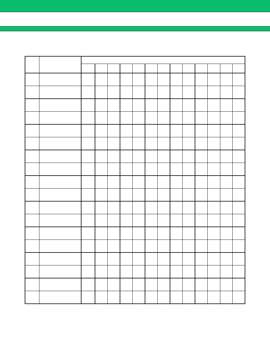
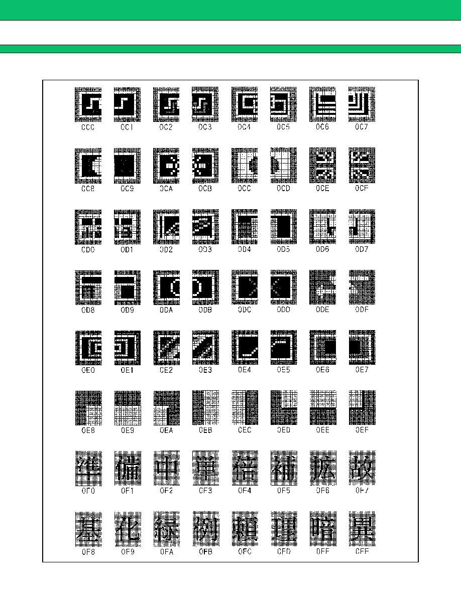
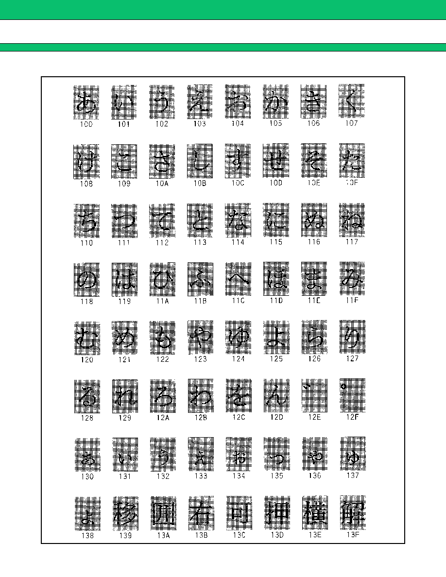
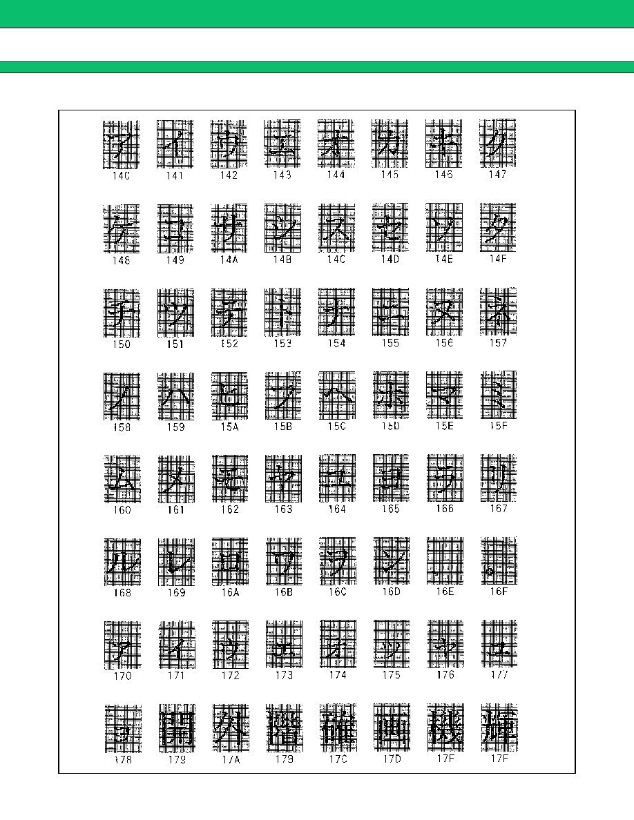
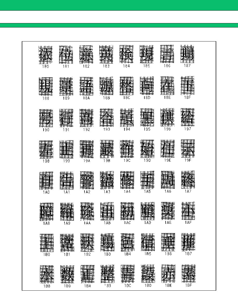
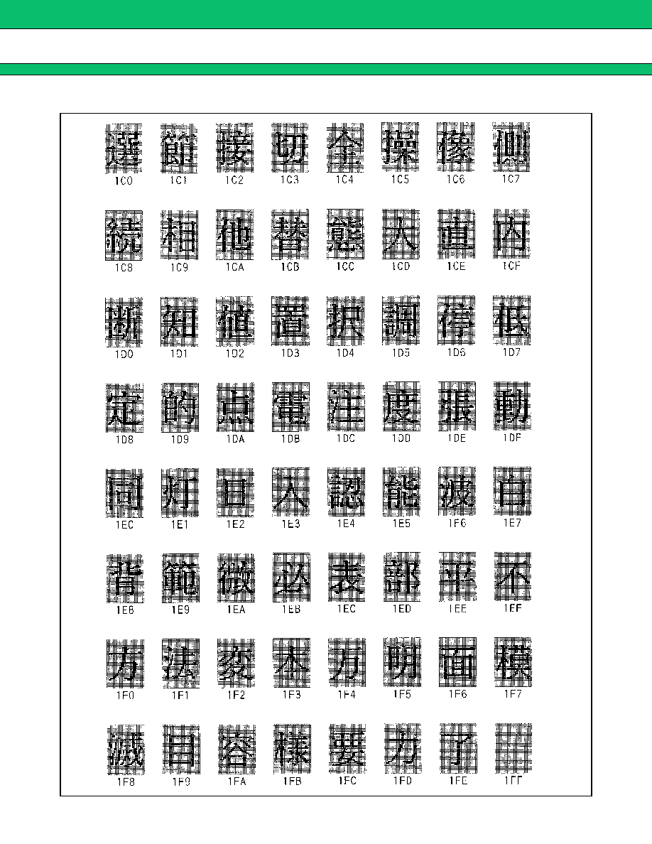
CONTENTS OF MB90098A-001 (STANDARD PRODUCT) FONT DATA
MB90098A
34
MB90098A
35
MB90098A
36
MB90098A
37
MB90098A
38
MB90098A
39
MB90098A
40

MB90098A
41
s
s
s
s
ORDERING INFORMATION
Part Number
Package
Remarks
MB90098APF
28-pin plastic SOP
(FPT-28P-M17)
MB90098A
42
s
s
s
s
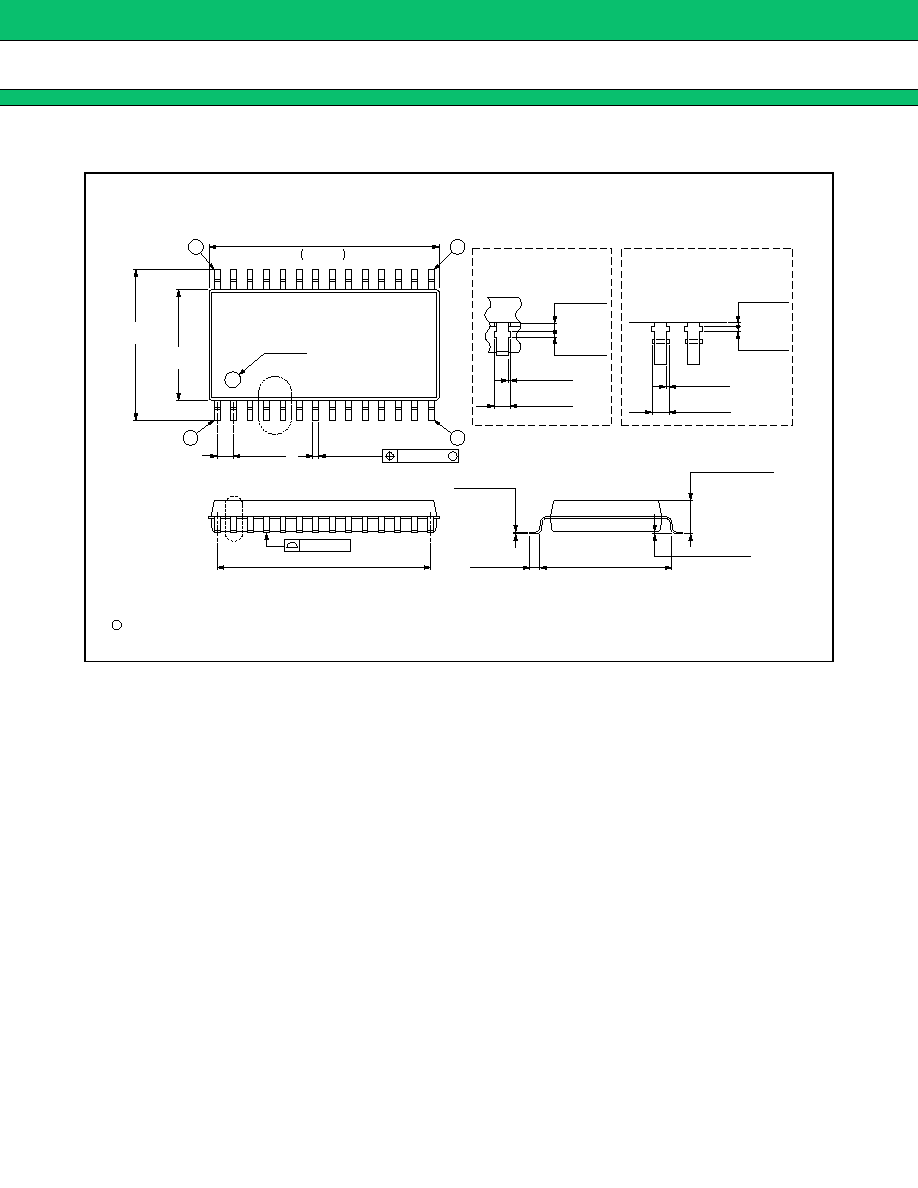
PACKAGE DIMENSION
28-pin plastic SOP
(FPT-28P-M17)
Dimensions in mm (inches)
C
2000 FUJITSU LIMITED F28048S-1C-2
.699
.008
+.010
0.20
+0.25
17.75
28
15
1
14
1.27(.050)
TYP
0.45±0.10
(.018±.004)
"A"
INDEX
16.51(.650)
REF
"B"
0.15±0.05
(.006±.002)
0.80±0.20
(.031±.008)
10.20±0.30
(.402±.012)
0(0)MIN
(STAND OFF)
2.80(.110)MAX
0.20(.008)
0.35(.014)
MAX
0.68(.027)
MAX
0.18(.007)
0.18(.007)
MAX
0.68(.027)
MAX
0.15(.006)
0.20(.008)
Details of "B" part
Details of "A" part
8.60±0.20
(.339±.008)
11.80±0.30
(.465±.012)
M
0.13(.005)
(Mounting height)
0.10(.004)

MB90098A
FUJITSU LIMITED
All Rights Reserved.
The contents of this document are subject to change without notice.
Customers are advised to consult with FUJITSU sales
representatives before ordering.
The information and circuit diagrams in this document are
presented as examples of semiconductor device applications, and
are not intended to be incorporated in devices for actual use. Also,
FUJITSU is unable to assume responsibility for infringement of
any patent rights or other rights of third parties arising from the use
of this information or circuit diagrams.
The products described in this document are designed, developed
and manufactured as contemplated for general use, including
without limitation, ordinary industrial use, general office use,
personal use, and household use, but are not designed, developed
and manufactured as contemplated (1) for use accompanying fatal
risks or dangers that, unless extremely high safety is secured, could
have a serious effect to the public, and could lead directly to death,
personal injury, severe physical damage or other loss (i.e., nuclear
reaction control in nuclear facility, aircraft flight control, air traffic
control, mass transport control, medical life support system, missile
launch control in weapon system), or (2) for use requiring
extremely high reliability (i.e., submersible repeater and artificial
satellite).
Please note that Fujitsu will not be liable against you and/or any
third party for any claims or damages arising in connection with
above-mentioned uses of the products.
Any semiconductor devices have an inherent chance of failure. You
must protect against injury, damage or loss from such failures by
incorporating safety design measures into your facility and
equipment such as redundancy, fire protection, and prevention of
over-current levels and other abnormal operating conditions.
If any products described in this document represent goods or
technologies subject to certain restrictions on export under the
Foreign Exchange and Foreign Trade Law of Japan, the prior
authorization by Japanese government will be required for export
of those products from Japan.
F0106
©
FUJITSU LIMITED Printed in Japan
Document Outline