Äîêóìåíòàöèÿ è îïèñàíèÿ www.docs.chipfind.ru
DS07-12551-2E
FUJITSU SEMICONDUCTOR
DATA SHEET
8-bit Proprietary Microcontrollers
CMOS
F
2
MC-8L MB89051 Series
MB89F051/MB89051
s
DESCRIPTION
The MB89051 series is a general-purpose, single-chip microcontroller that features a compact instruction set and
contains a range of peripheral function set and timers, serial interface, a PWM timer, the USB hub function and
the USB function. The USB hub function, in particular, supports five down ports (one of them is dedicated to an
internal function) allowing them to interface with other USB devices. The microcontrollers also contain one USB
function channel to support full speed.
s
FEATURES
· Package type
64-pin LQFP Package (0.65 mm pitch)
· High-speed operations at low voltage
Minimum execution time : 0.33
µ
s (Automatically generates a 12 MHz main clock and a 48 MHz USB interface
synchronization clock with an externally supplied 6 MHz clock and the internal PLL circuit.)
(Continued)
s
Package
64-pin plastic LQFP
(FPT-64P-M09)

MB89051 Series
2
· F
2
MC-8L CPU core
Instruction set that is optimum to the controllers
-Multiplication and division instructions
-16-bit arithmetic operations
-branch instructions by bit testing
-bit manipulation instructions, etc.
· PLL clock control
The internal PLL clock circuit allows the use of low-speed clocks which are advantageous to noise character-
istics.
(6 MHz externally-supplied clock
12 MHz internal system clock)
· Various timers
8-bit PWM timer (can be used as either 8-bit PWM timer 2 channels or PPG timer 1 channel)
Internal 21-bit timebase timer
· Internal USB transceiver circuit (Compatible with full and low speeds)
· USB hub
USB function Compliant to USB Protocol Revision 1.0
Five downstream port channels (One of these channels is dedicated to a function.)
Automatically responds to all USB protocols by hardware.
Descriptor configuration is provided as ROM data for automatic responding by hardware (Vender ID and product
ID) .
String data is not supported.
Allows switching between BUS power supply and own power supply mode.
Power supply to the USB down port is controlled port by port.
· USB function
USB function Compliant to USB Protocol Revision 1.0
Support for full speed when using hub
Support for both low and full speeds when using function
Allows four endpoints to be specified at maximum.
Types of transfer supported: control/interrupt/bulk/isochronous
Built-in DMAC (Maps the buffer for each endpoint on to the internal RAM to directly access the memory for
function's send and receive data.)
· UART/SIO, SIO Serial Interface
Built-in UART/SIO function (selectable by switching)
×
1 channel
Built-in SIO (3.3 V)
×
2 channels
· I
2
C interface*
1
Supports Philips I
2
C bus standards
Uses a two-wire data transfer protocol
Master/slave send/receive
· External interrupt
External interrupt (level detection
×
7 channels)
Seven inputs are independent of one another and can also be used for resetting from low-power consumption
mode (the L-level detection feature available) .
· Clock output functions
Able for 12 MHz*
2
and 6 MHz*
2
clocks to output. (dedicated pins, 3 V)
· Low power consumption (standby mode supported)
Stop mode (There is almost no current consumption since oscillation stops.)
Sleep mode (This mode stops the running CPU.)
(Continued)

MB89051 Series
3
(Continued)
· A maximum of 41 general-purpose I/O ports
General-purpose I/O ports (CMOS) : 37 (7 of 3 V ports)
General-purpose I/O ports (Nch open drain) : 4
· Power supply
Supply voltage: 3.3 V
±
0.3 V or 5.0 V
±
0.5 V
· Operating temperature
T
A
=
-
40
°
to
+
85
°
C (When the USB function is not in use.)
T
A
=
0
°
C to
+
70
°
C (When the USB function is in use.)
*1 : I
2
C license
The customer is licensed to use Philips I
2
C patent when using this product in an I
2
C system that complies with
the Philips I
2
C standard specifications.
*2 : When an external supply clock is at 6 MHz.
MB89051 Series
4
s
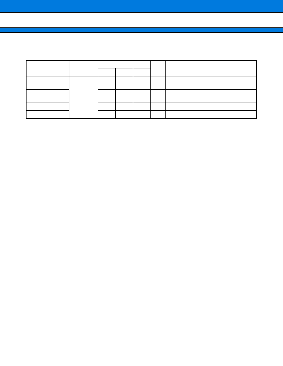
PRODUCT LINEUP
* : When external supply clock is at 6 MHz.
Part number
MB89051
MB89F051
Parameter
ROM size
32 KB
32 KB (FLASH)
RAM size
2 KB
Package
LQFP-64 (FPT-64P-M09)
Others
MASK product
FLASH product/EVA product
CPU functions
Number of instructions
Instruction bit length
Instruction length
Data bit length
Minimum execution time
Interrupt processing time
: 136
: 8 bits
: 1 to 3 bytes
: 1, 8, and 16 bits
: 0.33
µ
s (6 MHz)
: 3
µ
s (6 MHz)
General-
purpose ports
General purpose I/O ports (37 : CMOS (7 of 3 V ports ) , 4 : Nch open drain)
USB hub
Upstream port : 1 channel
Downstream port : 5 channels (One is dedicated to an internal function.)
Port power supply control method : By individual port
Allows selection between own power supply and bus power supply
USB function
Supports full speed : when using hub
Supports full and low speeds : when using function
End point max 4
Built-in DMAC (Can be set to DMA transfer to the internal RAM)
PWM timer
8-bit PWM timer operation 2 channels (can also be used as a PPG 1 channel timer)
UART
SIO
Allows switching between UART (clock-synchronous/asynchronous data transfer allowed)
and SIO (simple serial transfer).
SIO
SIO (simple serial)
×
2 channels (3 V)
I
2
C interface
One channel. Supports Phillips I
2
C bus standards. Uses a 2-wire protocol for communications
with other devices.
Timebase
timer
21-bit timebase timer
Clock output
Allows clock output of 12 MHz* and 6 MHz* (3 V)
Standby mode
Sleep mode and Stop mode
Peripheral functions
MB89051 Series
5
s
DIFFERENCES AMONG PRODUCTS
1.
Memory Size
· Before evaluating using the FLASH product, it is necessary to confirm its differences from the product that will
actually be used.
2.
Current Consumption
· When operating at low speed, FLASH products will consume more current than mask ROM products. However,
in sleep/stop mode the current consumption is the same.
· For detailed information on each package, see "
s
PACKAGE DIMENSIONS"
3.
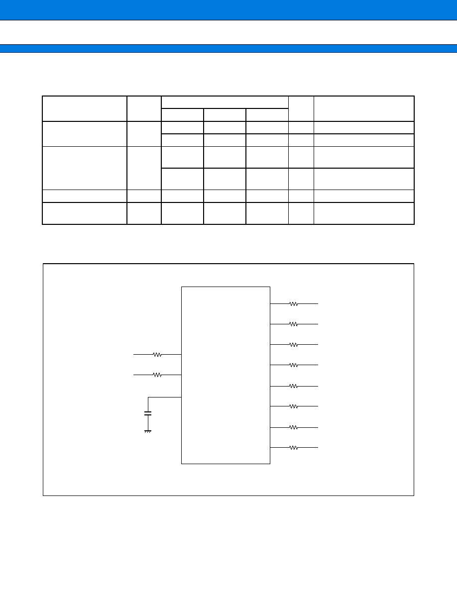
USB Pull-up Resistor control
· Remains in high impedance state until USB connection take place. Before the USB connection, use USBP
pin output to control pull-up resistance by software.
·
The example of connection
D
+
D
-
1.5 k
3.3 V
Host PC
MB89051 series
RPVP pin
RPVM pin
USBP pin
MB89051 Series
6
s
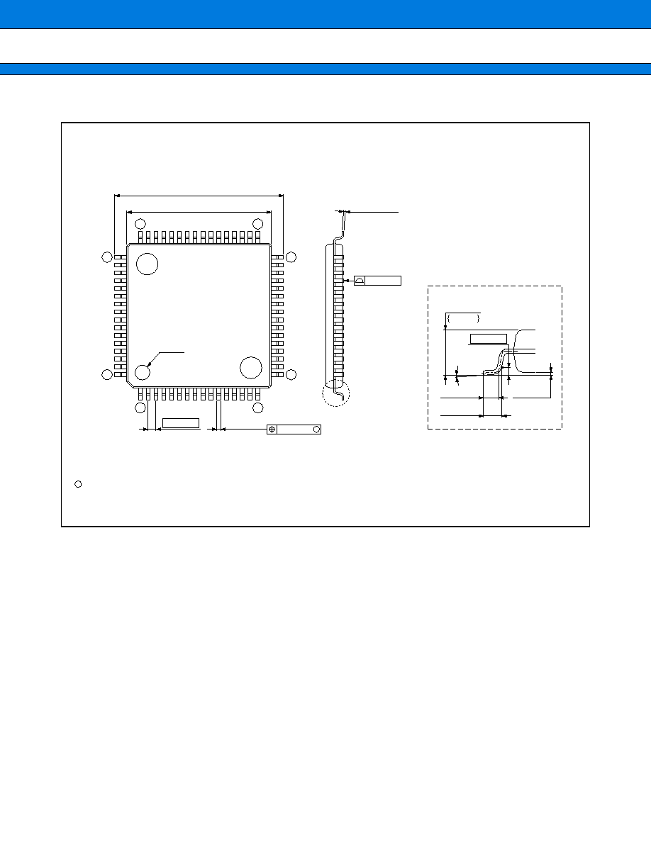
PIN ASSIGNMENT
(TOP VIEW)
(FPT-64P-M09)
P34/INT4/SCK1
P35/INT5/SCK2
P36/INT6/SO2
P37/INT7/SI2
CLK1
CLK2
P40/POW5
P41/POW2
P42/POW3
P43/POW4
P44/UCK
P45/UO
P46/UI/PWM1
V
SS
P47/PWM2
MOD2
1
2
3
4
5
6
7
8
9
10
11
12
13
14
15
16
P00
P01
P02
P03
P04
P05
P06
P07
P10
P11
P12
P13
P14
P15
P16
P17
48
47
46
45
44
43
42
41
40
39
38
37
36
35
34
33
P53/SDA
P54/SCL
RST
MOD0
MOD1
X0
X1
V
SS
P27
P26
P25
P24
P23
P22
P21
P20
17
18
19
20
21
22
23
24
25
26
27
28
29
30
31
32
P33/INT3/SO1
P32/INT2/SI1
P31/INT1
D4VM
D4VP
D3VM
D3VP
D2VM
D2VP
D5VM
D5VP
USBP
RPVM
RPVP
C
V
CC
64
63
62
61
60
59
58
57
56
55
54
53
52
51
50
49
MB89051 Series
7
s
PIN DESCRIPTION
(Continued)
Pin No.
Pin name
Circuit
type
Function
1
P34/INT4/
SCK1
E
General-purpose CMOS I/O pin
The external interrupt input is a hysteresis input. (Level detection)
SIO1 clock I/O
2
P35/INT5/
SCK2
E
General-purpose CMOS I/O pin
The external interrupt input is a hysteresis input. (Level detection)
SIO2 clock I/O
3
P36/INT6/
SO2
B
General-purpose CMOS I/O pin
The external interrupt input is a hysteresis input. (Level detection)
SIO2 serial data output
4
P37/INT7/SI2
E
General-purpose CMOS I/O pin
The external interrupt input is a hysteresis input. (Level detection)
SIO2 serial data input
5
CLK1
M
6 MHz clock output pin (When external supply clock is at 6 MHz.)
6
CLK2
M
12 MHz clock output pin (When external supply clock is at 6 MHz.)
7
P40/POW5
B
General-purpose CMOS I/O pin
This pin also serves as USB Down Port power control signal.
8
P41/POW2
B
General-purpose CMOS I/O pin
This pin also serves as USB Down Port power control signal.
9
P42/POW3
B
General-purpose CMOS I/O pin
This pin also serves as USB Down Port power control signal.
10
P43/POW4
B
General-purpose CMOS I/O pin
This pin also serves as USB Down Port power control signal.
11
P44/UCK
E
General-purpose CMOS I/O pin
UART/S10 clock I/O
12
P45/UO
B
General-purpose CMOS I/O pin
UART/S10 serial data output
13
P46/UI/
PWM1
N
Nch open drain general-purpose I/O pin
UART/S10 serial data input
PWM timer
14
V
SS
Power supply pin (GND)
15
P47/PWM2
K
Nch open drain general-purpose I/O pin
PWM timer
16
MOD2
F
An operating mode designation pin. Connect directly to Vss.
17
P53/SDA
K
Nch open drain general-purpose I/O pin
Also serve as I
2
C interface data input/output pin.
18
P54/SCL
K
Nch open drain general-purpose I/O pin
Also serve as I
2
C interface clock input/output pin.
19
RST
I
Reset pin (Reset on the negative logic low level.)
20
MOD0
F
An operating mode designation pin. Connect directly to Vss.
21
MOD1
F
An operating mode designation pin. Connect directly to Vss.
MB89051 Series
8
* : For output only on the emulator.
(Continued)
Pin No.
Pin name
Circuit
type
Function
22
X0
A
Pins for the connection of crystal oscillation circuit.(6 MHz)
23
X1
24
V
SS
Power supply pin (GND)
25
P27
B
General-purpose CMOS I/O pin*
26
P26
B
General-purpose CMOS I/O pin*
27
P25
B
General-purpose CMOS I/O pin*
28
P24
B
General-purpose CMOS I/O pin*
29
P23
B
General-purpose CMOS I/O pin*
30
P22
B
General-purpose CMOS I/O pin*
31
P21
B
General-purpose CMOS I/O pin*
32
P20
B
General-purpose CMOS I/O pin*
33
P17
B
General-purpose CMOS I/O pin
34
P16
B
General-purpose CMOS I/O pin
35
P15
B
General-purpose CMOS I/O pin
36
P14
B
General-purpose CMOS I/O pin
37
P13
B
General-purpose CMOS I/O pin
38
P12
B
General-purpose CMOS I/O pin
39
P11
B
General-purpose CMOS I/O pin
40
P10
B
General-purpose CMOS I/O pin
41
P07
B
General-purpose CMOS I/O pin
42
P06
B
General-purpose CMOS I/O pin
43
P05
B
General-purpose CMOS I/O pin
44
P04
B
General-purpose CMOS I/O pin
45
P03
B
General-purpose CMOS I/O pin
46
P02
B
General-purpose CMOS I/O pin
47
P01
B
General-purpose CMOS I/O pin
48
P00
B
General-purpose CMOS I/O pin
49
V
CC
Power supply pin.
50
C
Connect an external capacitor of 0.1
µ
F. When using with 3.3 V power
supply, connect this pin with the Vcc pin to set to 3.3 V input.
51
RPVP
USBDRV USB route port
+
pin
52
RPVM
USBDRV USB router port
-
pin
53
USBP
L
USB pull-up resistance connection pin.
54
D5VP
USBDRV USB down port 5
+
pin
55
D5VM
USBDRV USB down port 5
-
pin
MB89051 Series
9
(Continued)
Pin No.
Pin name
Circuit
type
Function
56
D2VP
USBDRV USB down port 2
+
pin
57
D2VM
USBDRV USB down port 2
-
pin
58
D3VP
USBDRV USB down port 3
+
pin
59
D3VM
USBDRV USB down port 3
-
pin
60
D4VP
USBDRV USB down port 4
+
pin
61
D4VM
USBDRV USB down port 4
-
pin
62
P31/INT1
B
General-purpose CMOS I/O pin
External interrupt input (Hysteresis input (level detection) )
63
P32/INT2/SI1
E
General-purpose CMOS I/O pin
External interrupt input (Hysteresis input (level detection) )
SIO1 serial data input
64
P33/INT3/
SO1
B
General-purpose CMOS I/O pin
External interrupt input (Hysteresis input (level detection) )
SIO1 serial data output
MB89051 Series
10
s
I/O CIRCUIT TYPE
(Continued)
Type
Circuit
Remarks
A
· Oscillation feedback resistance :
1 M
approx.
B
· CMOS I/O
E
· CMOS I/O
· Hysteresis input
F
· CMOS input
I
· Hysteresis I/O
· Pullup resistance
X1
X0
Stanby control signal
Pch
Pch
R
Nch
Pullup control register
Input
Stanby control
signal
Pch
Pch
R
Nch
Pullup control register
Resource input
Port input
Stanby
control signal
Input
Pch
R
Nch
Input
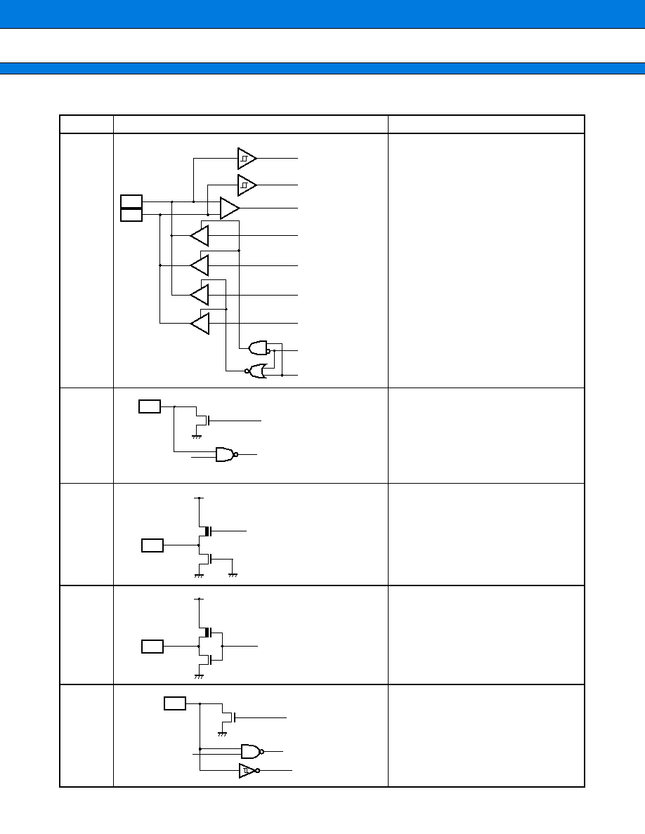
MB89051 Series
11
(Continued)
Type
Circuit
Remarks
USBDRV
· USB I/O
K
· Nch open drain I/O
L
· USB pull-up resistance connection
M
· Clock output
N
· Nch open drain I/O
· Hysteresis input
D
+
D
-
D
+
input
D
-
input
Differential input
Low D
-
output
Direction
Full D
-
output
Speed
Low D
+
output
Full D
+
output
Nch
Input
Stanby control
signal
Pch
Nch
Pch
Nch
Nch
Resource input
Port input
Stanby
control signal

MB89051 Series
12
s
HANDLING DEVICES
1.
Preventing Latchup
Latchup may occur on CMOS ICs if voltage higher than Vcc or lower than Vss is applied to input or output pins
other than the medium- and high-voltage pins or if voltage higher than the rating is applied between Vcc and Vss.
When latchup occurs, power supply current increases rapidly and might thermally damage elements.When
using, take great care not to exceed the absolute maximum ratings.
Also take care to prevent the analog input from exceeding the digital power supply (Vcc) when the power supply
to the analog power system is turned on and off.
2.
Treatment of Unused Input Pins
Leaving unused input pins open could cause malfunctions and latchup leading to permanent damage to the
pins.These unused pins should be connected to a pullup or pulldown resistance of at least 2 k
between the
pin and the power supply.
Unused I/O pins should be placed in output state to leave it open or pins that are in input state should be handled
the same as unused input pins.
3.
Note to noise in the External Reset Pin (RST)
If the reset pulse applied to the external reset pin (RST) does not meet the specifications, it may cause malfunc-
tions. Use caution so that the reset pulse less than the specifications will not be fed to the external reset pin (RST).
4.
Power Supply Voltage Fluctuations
Although Vcc power supply voltage is assured to operate within the rated range, a rapid fluctuation of the voltage
could cause malfunctions even if it occurs within the rated range. Stabilizing voltage supplied to the IC is therefore
important. As stabilization guidelines, it is recommended to control power so that Vcc ripple fluctuations (P-P
value) will be less than 10% of the standard V
CC
value at the commercial frequency (50 Hz to 60 Hz) and the
transient fluctuation rate will be less than 0.1 V/ms at the time of a momentary fluctuation such as when power
is switched.
5.
Note on the clock during operation
This microcontroller uses a PLL for generating the main clock signal. If the oscillator is removed or the clock
input stops during operation, therefor, the microcontroller may keep on operating at the free-running frequency
of the self-oscillation circuit in the PLL. The operation is not however guaranteed.
6.
About port 2 (P20 to P27)
Port 2 serves as an output-only terminal on the emulator.
MB89051 Series
13
s
PROGRAMMING AND ERASING FLSH MEMORY
1.
Flash Memory
The flash memory is located between 8000
H
and FFFF
H
in the CPU memory map and incorporates a flash
memory interface circuit that allows read access and program access from the CPU to be performed in the same
way as mark ROM. Programming and erasing flash memory is also performed via the flash memory interface
circuit by executing instructions in the CPU. This enables the flash memory to be updated in place under the
control of the CPU, providing an efficient method of updating program and data.
2.
Flash Memory Features
· 32 Kbyte
×
8-bit configuration (16 K
+
8 K
+
8 K sectors)
· Automatic programming algorithm (Embedded Algorithm* : Equivalent to MBM29LV200)
· Includes an erase pause and restart function
· Data polling and toggle bit for detection of program/erase completion
· Detection of program/erase completion via CPU interrupt
· Compatible with JEDEC-standard command
· Sector Protection (sectors can be combined in any combination)
· No. of program/erase cycles : 10,000 (Min)
* : Embedded Algorithm is a trademark of Advanced Micro Devices.
3.
Procedure for Programming and Erasing Flash Memory
Programming and reading flash memory cannot be performed at the same time. Accordingly, to program or
erase flash memory, the program must first be copied from flash memory to RAM so that programming can be
performed without program access from flash memory.
4.
Flash Memory Register
·
Control status register (FMCS)
5.
Sector Configuration
The table below shows the sector configuration of flash memory and lists the addresses of each sector for both
during CPU access and a flash memory programming.
·
Sector configuration of flash memory
* : Programmer address
The programmer address is the address to be used instead of the CPU address when programming data from
a parallel flash memory programmer. Use the programmer address on programming or erasing using a general-
purpose parallel programmer.
Flash Memory
CPU Address
Programmer Address*
16 Kbytes
FFFF
H
to C000
H
1FFFF
H
to 1C000
H
8 Kbytes
BFFF
H
to A000
H
1BFFF
H
to 1A000
H
8 Kbytes
9FFF
H
to 8000
H
19FFF
H
to 18000
H
R
R/W
R/W
RDY
bit7
bit6
bit5
bit4
bit3
bit2
bit1
bit0
002E
H
000X00X0
B
R/W
R/W
R/W
R/W
INTE
RDYINT
WE
Re-
served
Re-
served
Re-
served
Initial value
Address

MB89051 Series
14
6.
ROM Programmer Adaptor and Recommended ROM Programmers
· Inquiry:
Package
Compatible adapter
Compatible programmers and models
Sunhayato Corp.
Ando Denki K.K.
FPT-64P-M09
FLASH-64QF2-32DP-8LF3
AF9708 (ver 1.60 or higher)
AF9709 (ver 1.60 or higher)
Sunhayato Corp.
: TEL
: 81-3-3984-7791
FAX
: 81-3-3971-0535
E-mail : adapter@sunhayato.co.jp
Ando Denki K. K.
: TEL
: 81-3-3733-1160
MB89051 Series
15
s
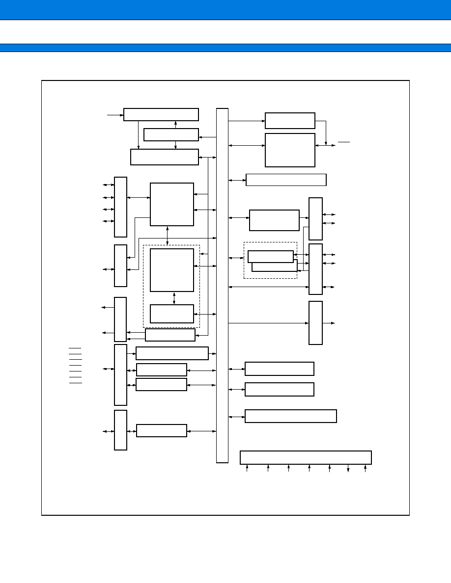
BLOCK DIAGRAM
RPVP
RPVM
D2VP
D5VP
D2VM
D5VM
USB DRV
Rp
Dp2-5
Dp1
CMOS I/O Port
3 V CMOS I/O Port
CMOS out Port
CMOS I/O Port
Nch I/O Port
P40/POW5
P41/POW2
P42/POW3
P43/POW4
DMAC
P53/SDA, P54/SCL
V
SS
V
CC
MOD0 MOD1
C
RAM 2 KByte
F
2
MC - 8L CPU
ROM 32 K / FLASH 32 KByte
P20
P27*
P45/UO
P44/UCK
P47/PWM2
P46/UI/PWM1
P00
P07, P10
P17
SIO
RST
X0
X1
CLK2
3 V CLK Port
CLK1
I2C
SIO1
SIO2
P31/INT1
P32/INT2/SI1
P33/INT3/SO1
P34/INT4/SCK1
P35/INT5/SCK2
P36/INT6/SO2
P37/INT7/SI2
MOD2 USBP
UART
Nch I/O Port
Main clock oscillator
Clock control circuit
PLL circuit
Internal Bus
USB
Function
Circuit
Clock output
External interrupt (level)
Reset output
Power on
reset circuit
(watchdog
timer)
21-bit timebase timer
8 bit PWM
timer
Other pins
USB HUB
Circuit
* : Port 2 serves as an output-only terminal on the emulator.
MB89051 Series
16
s
CPU CORE
1.
Memory Size
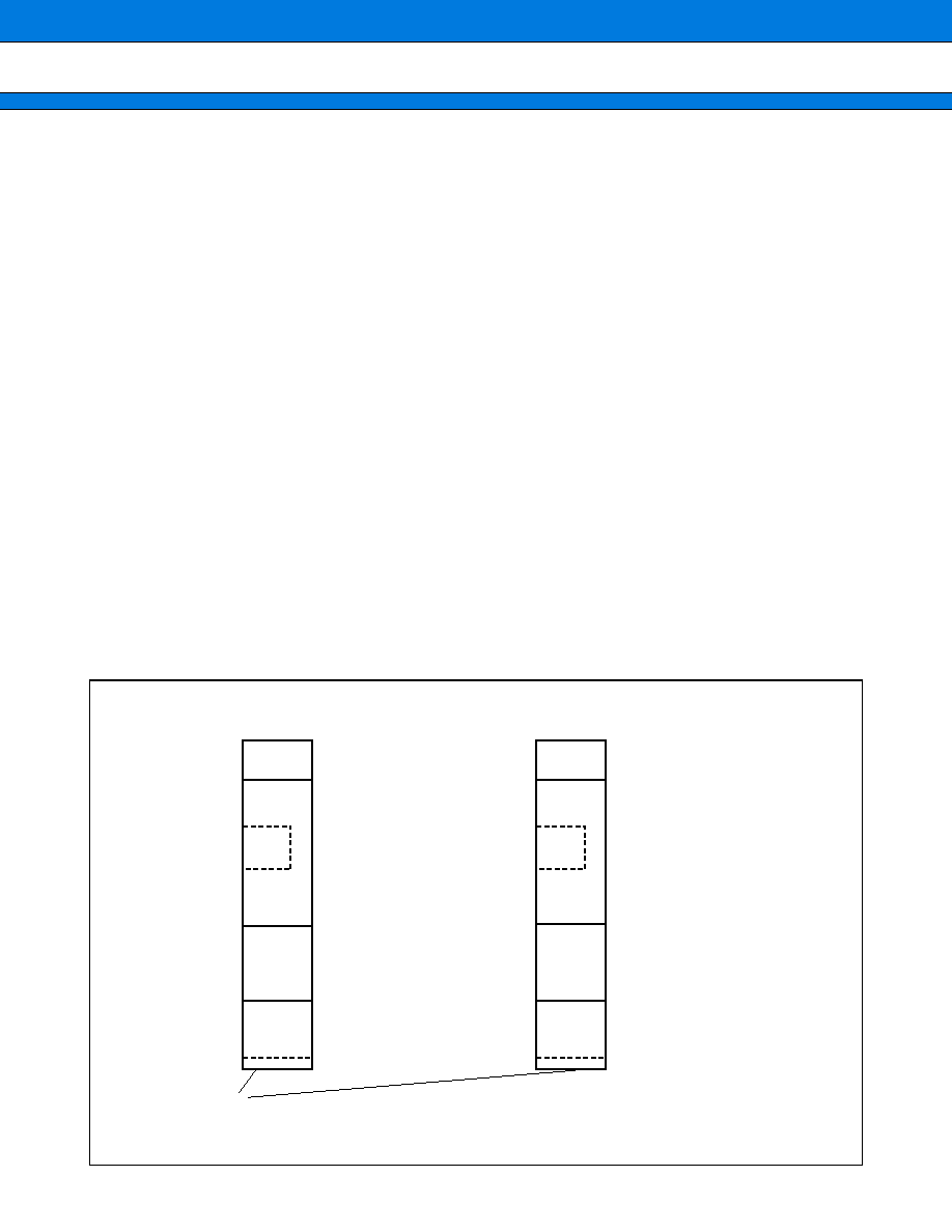
The MB89051 microcontroller offers a memory space of 64 Kbytes consisting of the I/O, RAM and ROM areas.
The memory space contains areas that are used for specific purposes, such as a general-purpose register and
a vector table.
· I/O area (addresses: 0000
H
through 007F
H
)
This area is assigned with the control and data registers, for example, of peripheral functions to be built in.
The I/O area is as accessible as the memory since the area is assigned to a part of the memory space.Direct
addressing also allows the area to be accessed faster.
· RAM area
As an internal data area, a static RAM is built in.
The internal RAM capacity varies with the product type.
The area 80
H
to FF
H
can be accessed at high speed with direct addressing.
The area 100H to 1FFH can be used a general-purpose register area. (The usable area is limited depending
on the product.)
When reset, RAM data becomes undefined.
· ROM area
As an internal program area, a ROM is built in.
The internal RAM capacity varies with the product type.
The area FFC0
H
to FFFF
H
should be used for a vector table, for example.
·
·
·
·
Memory map
MB89051
0000
H
0080
H
0100
H
0200
H
0880
H
8000
H
FFC0
H
FFFF
H
ROM
I/O
RAM
MB89F051
0000
H
0080
H
0100
H
0200
H
0880
H
8000
H
FFC0
H
FFFF
H
ROM
I/O
RAM
Register
Access
prohibited
Vector table
(reset, interrupt and vector call instructions)
* : FLASH ROM
Register
Access
prohibited
MB89051 Series
17
2.
Registers
The MB89051 series has two types of registers; the registers dedicated to specific purposes in the CPU and
the general-purpose registers.
The dedicated registers are as follows:
The PS register can further be divided into the register bank pointer in the higher 8 bits (RP) and the condition
code register in the lower 8 bits (CCR). (See the diagram below.)
Program counter (PC)
: A 16-bit register to indicate locations where instructions are stored.
Accumulator (A)
:
A 16-bit register for temporary storage of operations. In the case of an 8-bit
data processing instruction, the lower one byte is used.
Temporary accumulator (T)
:
A 16-bit register which performs operations with the accumulator.In the case of
an 8-bit data processing instruction, the lower one byte is used.
Index register (IX)
: A 16-bit register for index modification.
Extra pointer (EP)
: A 16-bit register to point to a memory address.
Stack pointer (SP)
: A 16-bit register to indicate a stack area.
Program status (PS)
: A 16-bit register to store a register pointer or a condition code.
PS
PC
A
T
IX
EP
SP
RP
CCR
16 bits
: Program counter
: Accumulator
: Temporary accumulator
: Index register
: Extra pointer
: Stack pointer
: Program status
FFFD
H
Initial value
Indeterminate
Indeterminate
Indeterminate
Indeterminate
Indeterminate
I-flag = 0, IL1, 0 = 11
Initial values for other bits are
indeterminate.
PS
RP
CCR
X011XXXX
B
bit15 bit14 bit13 bit12 bit11 bit10
bit9
bit8
bit7
bit6
bit5
bit4
bit3
bit2
bit1
bit0
R4
R3
R2
R1
R0
-
-
-
H
I
IL1
IL0
N
Z
V
C
CCR initial value
H-flag
IL 1,0
I-flag
N-flag
Z-flag
V-flag
C-flag
X: Undefined
MB89051 Series
18
The RP points to the address of the register bank currently in use. The relationship between the pointer contents
and the actual address is based on the conversion rule shown next.
The CCR consists of the bits indicating arithmetic operation results or transfer data contents and the bits that
control CPU operations at the time of an interrupt.
H flag
: The flag is set to "1" when an arithmetic operation results in a carry from bit 3 to bit 4 or in a borrow
from bit 4 to bit 3. The bit is cleared to "0" in other instances.The flag is for decimal adjustment
instructions; do not use for other than additions and subtractions.
I flag
: Interrupt is enabled when this flag is set to "1." Interrupt is disabled when this flag is set to "0." The
flag is set to "0" when reset.
IL1, 0
:
Indicates the level of the interrupt currently enabled.An interrupt is processed only if its level is
higher than the value this bit indicates.
IL1
IL0
Interrupt level
High-low
0
0
1
Higher
Lower = no interruption
0
1
1
0
2
1
1
3
N flag
: The flag is set to "1" when an arithmetic operation results in setting of the MSB to "1" or is cleared
to "0" when the MSB is set to "1."
Z flag
: The flag is set to "1" when an arithmetic operation results in "0" or is set to "0" in other instances.
V flag
: The flag is set to "1" when an arithmetic operation results in two's complement overflow or is
cleared to "0" if no overflow occurs.
C flag
: The flag is set to "1" when an arithmetic operation results in a carry from bit 7 or in a borrow to bit
7. The flag is cleared to "0" if neither of them occurs. In the case of a shift instruction, the flag is
set to the shift-out value.
Rule for Conversion of Actual Addresses in the General-purpose Register Area
"0"
"0"
"0"
"0"
"0"
"0"
"0"
"1"
R4
R3
R2
R1
R0
b2
b1
b0
A7
A6
A5
A4
A3
A2
A1
A0
A15 A14 A13 A12 A11 A10
A9
A8
Generated address
RP higher bits
OP code lower bits
MB89051 Series
19
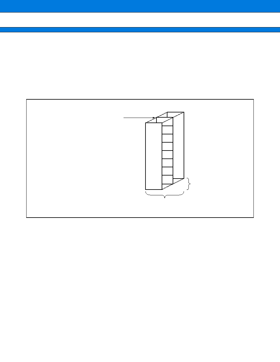
The following general-purpose registers are provided:
·General-purpose registers : 8-bit data storage registers
The general-purpose registers are 8 bits in length and located in the register banks in the memory.One bank
contains eight registers and the MB89051 microcontrollers allow a total of 16 banks to be used at maximum.
The bank currently in use is indicated by the register bank pointer (RP).
Register Bank Configuration
R0
R1
R2
R3
R4
R5
R6
R7
This address = 0100
H
+ 8
×
(RP)
Memory area
16 banks
MB89051 Series
20
s
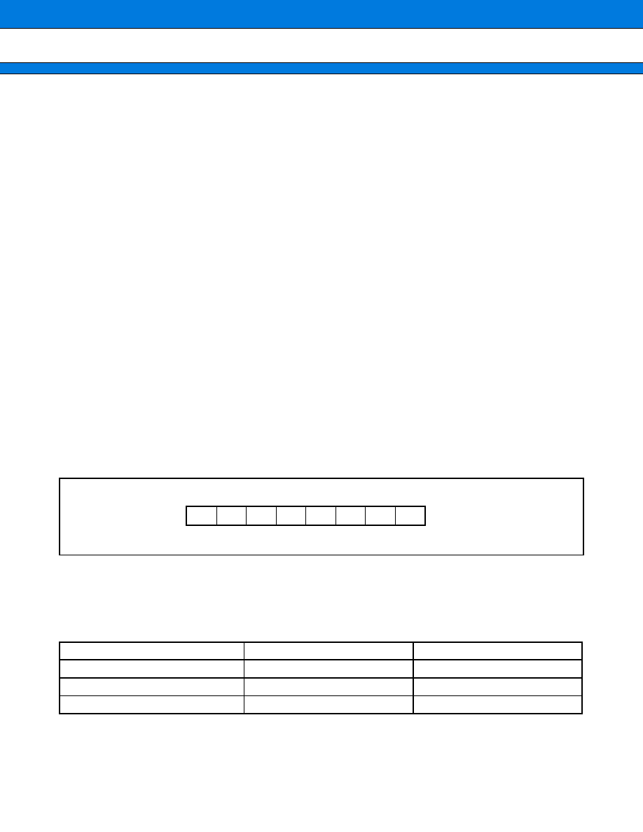
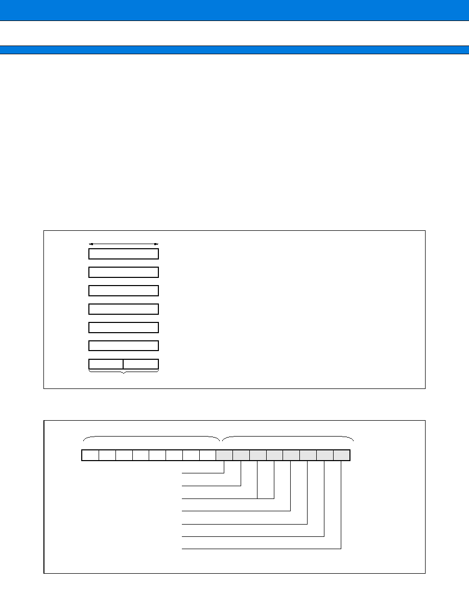
I/O MAP
(Continued)
Address
Register
name
Register description
Read/write
Initial value
00
H
PDR0
Port 0 data register
R/W
XXXXXXXX
01
H
DDR0
Port 0 direction register
W
0 0 0 0 0 0 0 0
02
H
PDR1
Port 1 data register
R/W
XXXXXXXX
03
H
DDR1
Port 1 direction register
W
0 0 0 0 0 0 0 0
04
H
PDR2
Port 2 data register
R/W
0 0 0 0 0 0 0 0
05
H
Reserved area
06
H
DDR2
Port 2 direction register
R/W
0 0 0 0 0 0 0 0
07
H
SYCC
System clock control register
R/W
XXX
1
1
X
0
0
08
H
STBC
Standby control register
R/W
0 0 0 1 XXXX
09
H
WDTC
Watchdog timer control register
R/W
XXXXXXXX
0A
H
TBTC
Timebase timer control register
R/W
0 0 XXX 0 0 0
0B
H
Vacancy
0C
H
PDR3/USBP
Port 3 data register/Pull-up register for USB
R/W
XXXXXXXX
0D
H
DDR3/USBPC
Port 3 data direction register/
Pull-up control register for USB
R/W
0 0 0 0 0 0 0 0
0E
H
Reserved area
0F
H
Vacancy
10
H
PDR4
Port 4 data register
R/W
XXXXXXXX
11
H
DDR4
Port 4 direction register
R/W
0 0 0 0 0 0 0 0
12
H
PDR5
Port 5 data register
R/W
XXX 1 1 XXX
13
H
to 15
H
Reserved area
16
H
to 20
H
Vacancy
21
H
PURR0
Port 0 pullup option setting register
R/W
1 1 1 1 1 1 1 1
22
H
PURR1
Port 1 pullup option setting register
R/W
1 1 1 1 1 1 1 1
23
H
PURR2
Port 2 pullup option setting register
R/W
1 1 1 1 1 1 1 1
24
H
PURR3
Port 3 pullup option setting register
R/W
1 1 1 1 1 1 1 X
25
H
PURR4
Port 4 pullup option setting register
R/W
1 1 1 1 1 1 1 1
26
H
Reserved area
27
H
CTR1
PWM control register 1
R/W
0 0 0 0 0 0 0 0
28
H
CTR2
PWM control register 2
R/W
0 0 0 X 0 0 0 0
29
H
CTR3
PWM control register 3
R/W
X 0 0 0 XXXX
2A
H
CMR1
PWM compare register 1
W
XXXXXXXX
2B
H
CMR2
PWM compare register 2
W
XXXXXXXX
2C
H
CKR
Clock output control register
R/W
XXXXXXX 0 0
2D
H
SCS
Serial clock switching register
R/W
XXXXXXX 0
MB89051 Series
21
(Continued)
Address
Register
name
Register description
Read/write
Initial value
2E
H
FMCS
Flash memory control status register
(Only built-in Flash Memory products)
R, R/W
0 0 0 X 0 0 X 0
2F
H
SMC1
Serial mode control register 1
R/W
0 0 0 0 0 0 0 0
30
H
SMC2
Serial mode control register 2
R/W
0 0 0 0 0 0 0 0
31
H
SSD
Serial status and control register
R
0 0 0 0 1 XXX
32
H
SIDR/SODR
Serial input/serial output data register
R/W
XXXXXXXX
33
H
SRC
Serial rate control register
R/W
XXXXXXXX
34
H
IBSR
I
2
C bus status register
R
0 0 0 0 0 0 0 0
35
H
IBCR
I
2
C bus control register
R/W
0 0 0 1 1 0 0 0
36
H
ICCR
I
2
C clock regeister
R/W
0 X 0 XXXXX
37
H
IADR
I
2
C address register
R/W
XXXXXXXX
38
H
IDAR
I
2
C data register
R/W
XXXXXXXX
39
H
Vacancy
3A
H
SMR1
Serial mode register 1
R/W
0 0 0 0 0 0 0 0
3B
H
SDR1
Serial data register 1
R/W
XXXXXXXX
3C
H
EIE
External interrupt control register
R/W
0 0 0 0 0 0 0 0
3D
H
EIF
External interrupt flag register
R/W
XXXXXXX 0
3E
H
, 3F
H
Vacancy
40
H
HMDR
HUB mode register
R/W
1 0 XXXXX 0
41
H
HDSR1
Hub descriptor register 1
R/W
XXXXXXXX
42
H
HDSR2
Hub descriptor register 2
R/W
XXXXXXXX
43
H
HDSR3
Hub descriptor register 3
R/W
XXXXXXXX
44
H
HSTR
Hub status register
R/W
0 0 0 0 0 0 0 0
45
H
OCCR
Over current register
R/W
0 XXX 0 0 0 0
46
H
DADR
Descriptor ROM address register
R/W
XXXXXXXX
47
H
Reserved area
48
H
, 49
H
Vacancy
4A
H
SMR2
Serial mode register 2
R/W
0 0 0 0 0 0 0 0
4B
H
SDR2
Serial data register 2
R/W
XXXXXXXX
4C
H
, 4D
H
Vacancy
4E
H
HDSR4
Hub descriptor register 4
R/W
0 0 0 0 0 1 01
4F
H
Vacancy
50
H
UMDR
USB reset mode register
R/W
1 0 0 0 XX 0 0
51
H
DBAR
DMA base address register
R/W
XXXXXXXX
52
H
TDCR0
Transfer data count register 0
R/W
X 0 0 0 0 0 0 0
53
H
TDCR1
Transfer data count register 1
R/W
X 0 0 0 0 0 0 0
54
H
Reserved area
55
H
TDCR21
Transfer data count register 2
R/W
X 0 0 0 0 0 0 0
MB89051 Series
22
(Continued)
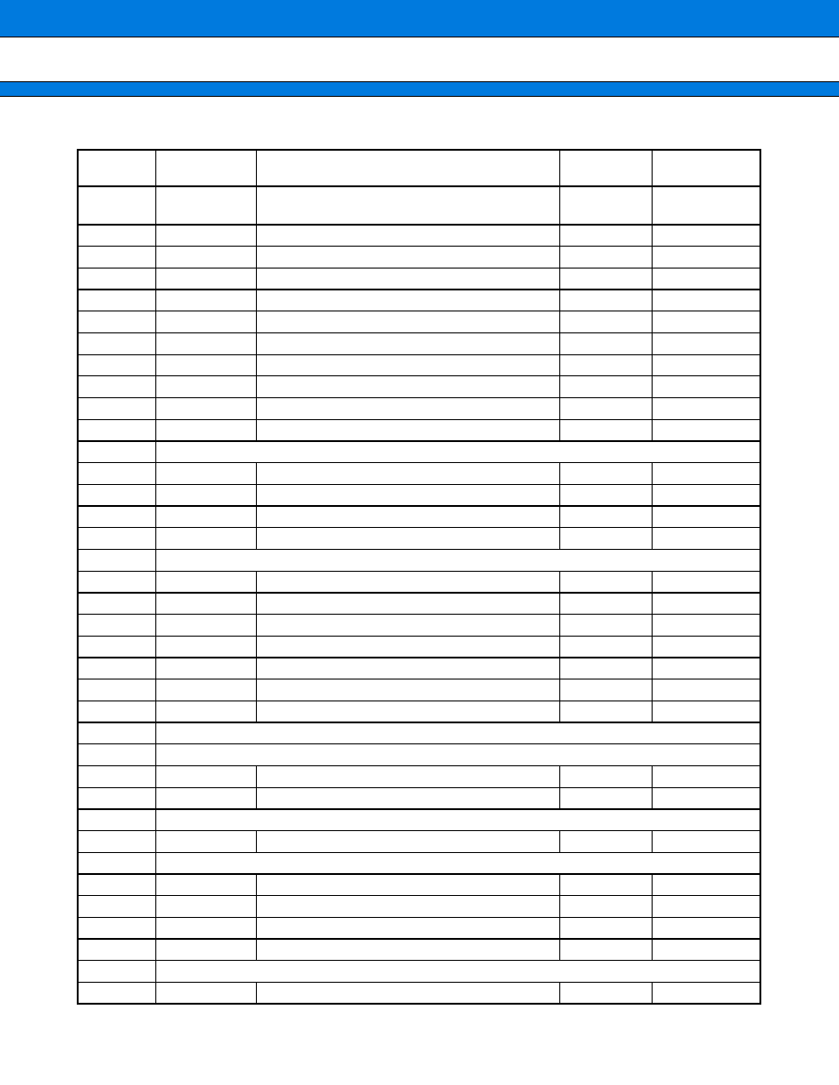
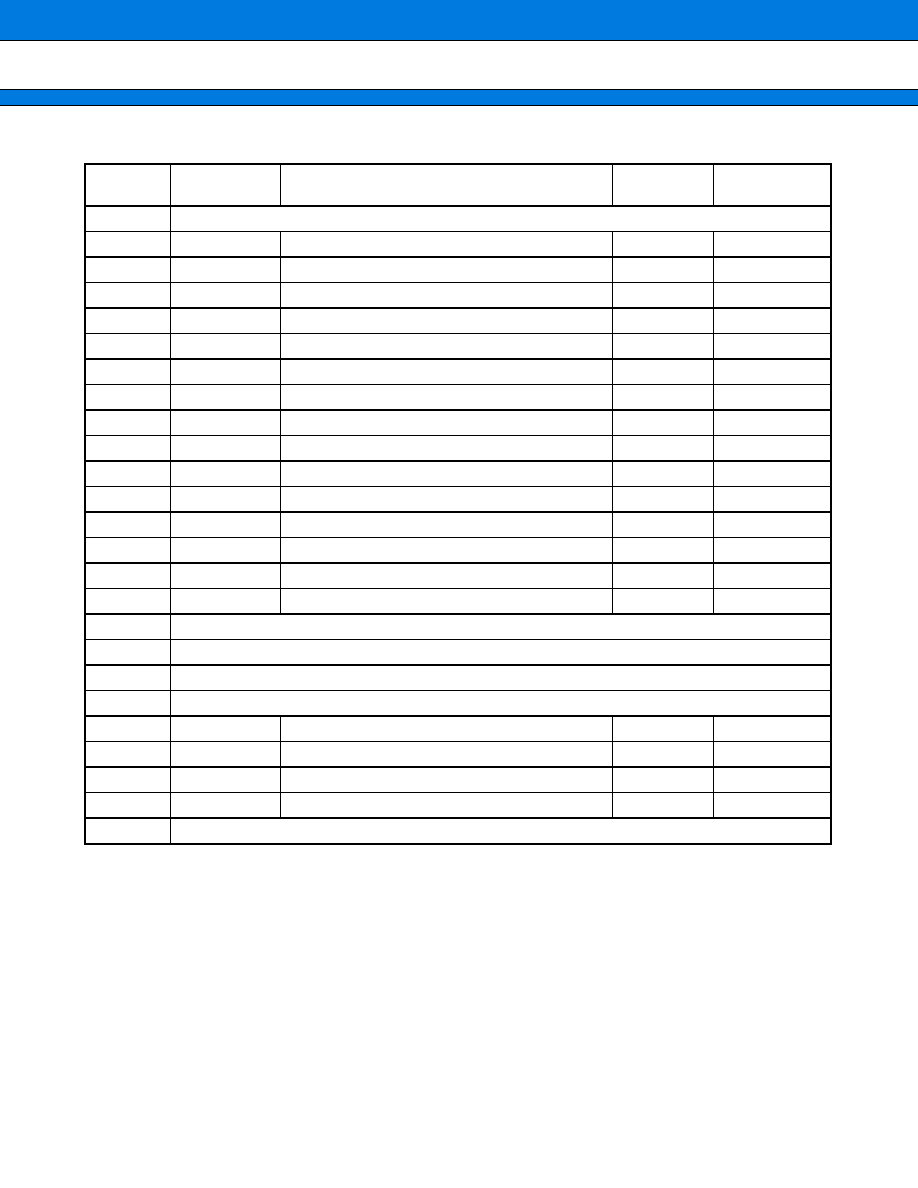
· Information about read/write
R/W
:
Read/write enabled, R
:
Read only, W
:
Write only
· Information about initial values
0: The initial value of this bit is "0".
1: The initial bit of this bit is "1".
X: The initial value of this bit is undefined.
Note : Vacancies and reserved spaces are not for use.
Address
Register
name
Register description
Read/write
Initial value
56
H
Reserved area
57
H
TDCR3
Transfer data count register 3
R/W
X 0 0 0 0 0 0 0
58
H
UCTR
USB control register
R/W
0 0 0 0 0 0 0 0
59
H
USTR1
USB status register 1
R/W
0 0 0 0 0 0 0 0
5A
H
USTR2
USB status register 2
R
XXXXXX 0 0
5B
H
UMSKR
USB interrupt mask register
R/W
0 0 0 0 0 0 0 0
5C
H
UFRMR1
USB frame status register 1
R
XXXXXXXX
5D
H
UFRMR2
USB frame status register 2
R
XXXXXXXX
5E
H
EPER
USB endpoint enable register
R/W
XXXX 0 0 0 1
5F
H
EPBR0
End point setup register 0
R/W
X 0 0 0 0 0 0 0
60
H
EPBR11
Endpoint setup register 11
R/W
XX 0 0 0 0 XX
61
H
EPBR12
Endpoint setup register 12
R/W
X 0 0 0 0 0 0 0
62
H
EPBR21
Endpoint setup register 21
R/W
XX 0 0 0 0 XX
63
H
EPBR22
Endpoint setup register 22
R/W
X 0 0 0 0 0 0 0
64
H
EPBR31
Endpoint setup register 31
R/W
XX 0 0 0 0 XX
65
H
EPBR32
Endpoint setup register 32
R/W
X 0 0 0 0 0 0 0
66
H
Reserved area
67
H
to 78
H
Vacancy
79
H
Reserved area
7A
H
Vacancy
7B
H
ILR1
Interrupt level setting register 1
W
1 1 1 1 1 1 1 1
7C
H
ILR2
Interrupt level setting register 2
W
1 1 1 1 1 1 1 1
7D
H
ILR3
level setting register 3
W
1 1 1 1 1 1 1 1
7E
H
ILR4
Interrupt level setting register 4
W
1 1 1 1 1 1 1 1
7F
H
Reserved area
MB89051 Series
23
s
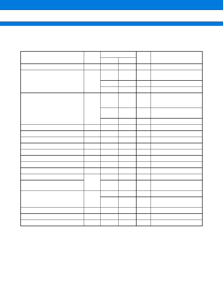
ELECTRICAL CHARACTERISTICS
1.
Absolute Maximum Ratings
(V
SS
=
0 V)
WARNING: Semiconductor devices can be permanently damaged by application of stress (voltage, current,
temperature, etc.) in excess of absolute maximum ratings. Do not exceed these ratings.
*1 : V
I
should not exceed the specified ratings. However, if the maximum current to /from an input is limited by some
means with external components, the I
CLAMP
rating supersedes the V
I
rating.
*2 : Maximum output current is defined as the peak value at one curresponding pin.
*3 : Average output current is defined as the average current flowing through one corresponding pin in an internal
of 100 ms. (Average value : operating current
×
operating duty)
Parameter
Symbol
Rating
Unit
Remarks
Min
Max
Power supply voltage
V
CC
V
SS
-
0.3
V
SS
+
6.0
V
Input voltage
V
I
V
SS
-
0.3
V
CC
+
0.3
V
Other than P31 to P37, P46,
P47, P53, P54*
1
V
SS
-
0.3
3.3
V
P31 to P37
V
SS
-
0.3
V
SS
+
6.0
V
P46,P47,P53, P54*
1
Output voltage
V
O
V
SS
-
0.3
V
CC
+
0.3
V
Other than P31 to P37, P46,
P47, P53, P54,
CLK1, CLK2, USBP
V
SS
-
0.3
3.6
V
P31 to P37, CLK1, CLK2,
USBP
V
SS
-
0.3
V
SS
+
6.0
V
P46, P47, P53, 54
Maximum clamp current
I
CLAMP
-
2.0
2.0
mA
*5
Total maximum clamp cuurent
|I
CLAMP
|
20
mA
*5
"L" level maximum output current
I
OL
15
mA
Normal output*
2
"L" level average output current
I
OLAV
4
mA
Normal output*
3
"L" level total maximum output current
I
OL
100
mA
Total normal output
"L" level total average output current
I
OLAV
40
mA
Total normal output*
4
"H" level maximum outputcurrent
I
OH
-
15
mA
Normal output*
2
"H" level average outputcurrent
I
OHAV
-
4
mA
Normal output*
3
"H" level total maximum output current
I
OH
-
50
mA
Total normal output
"H" level maximum outputcurrent
-
10
mA
Total output of P31 to P37,
CLK1, CLK2, USBP.
"H" level average total output currnt
I
OHAV
-
20
mA
Total normal output*
4
-
10
mA
Total output of P31 to P37,
CLK1, CLK2 and USBP.*
4
Power consumption
P
D
300
mW
Operating temperature
T
A
-
40
+
85
°
C
Storage temperature
Tstg
-
55
+
150
°
C
MB89051 Series
24
*4 : Average total output current is defined as the average current flowing through all corresponding pins in an
internal of 100 ms.
*5 :
·
Applicable to pins : P00 to P07, P10 to P17, P20 to P27, P40 to P45
·
Use within recommended operating conditions.
·
Use at DC voltage (current)
·
The
+
B signal should always be applied with a limiting resistance placed between the
+
B signal and the
microcontroller.
·
The value of the limiting resistance should be set so that when the
+
B signal is applied the input current
to the microcontroller pin does not exceed rated values, either instaneously or for prolonged periods.
·
Note that when the microcontroller drive current is low, such as in the power saving modes, the
+
B input
potentional may pass through the protective diode and increase the potentional at the V
CC
pin, and this may
affect other devices.
·
Note that if a
+
B signal is input when the microcontroller current is off (not fixed at 0 V) , the power supply
is provided from the pins, so that incomplete operation may result.
·
Note that if the
+
B input is applied during power-on, the power supply is provided from the pins and the
resulting supply voltage may not be sufficient to operate the power-on result.
·
Care must be taken not to leave the
+
B input pin open.
·
Note that analog system input pins other than the A/D input pins (LCD drive pins, comparator input pins, etc.)
cannot accept
+
B signl input.
·
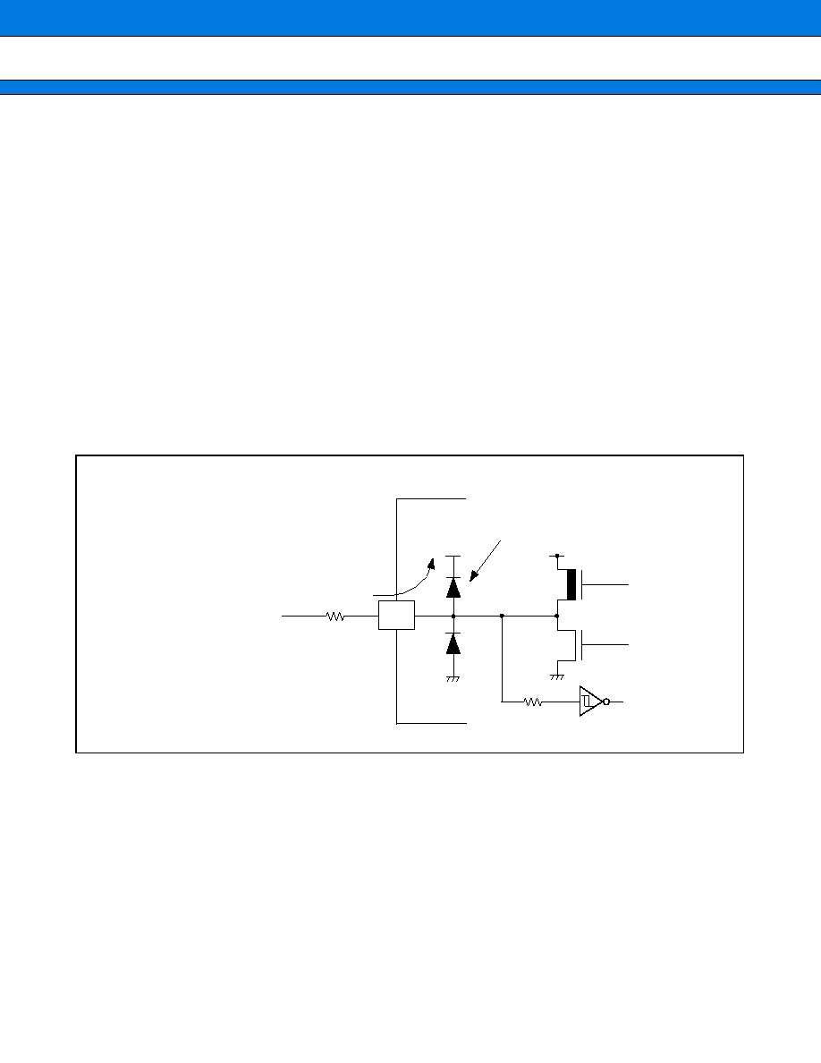
Sample recommended circuits :
WARNING: Semiconductor devices can be permanently damaged by application of stress (voltage, current,
temperature, etc.) in excess of absolute maximum ratings. Do not exceed these ratings.
P-ch
N-ch
R
V
CC
·
Input/Output Equivalent circuits
Protective diode
Limiting
resistance
+B input (0 V to 16 V)
MB89051 Series
25
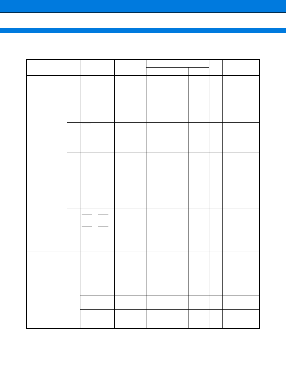
2.
Recommended Operating Conditions
(V
SS
=
0 V)
*: Use either a ceramic capacitor or a capacitor with similar frequency characteristics.The capacity of the smoothing
capacitor for the Vcc pin should be greater than that of the Cs.When using with a supply voltage of 3.3 V, connect
pin C with Vcc to input 3.3 V.
Parameter
Symbol
Value
Unit
Remarks
Min
Typ
Max
Power supply voltage
V
CC
4.5
5.5
V
At V
CC
=
5.0 V
3.0
3.6
V
At V
CC
=
3.3 V*
Operating temperature
T
A
-
40
+
85
°
C
When the USB function is not
in use.
0
+
70
°
C
When the USB function is in
use
Smoothing capacitor
C
S
0.1
1.0
µ
F
At V
CC
=
5.0 V*
Series resistance
R
S
16
When the USB function is in
use
R
S
R
S
R
S
R
S
R
S
R
S
R
S
R
S
R
S
R
S
C
S
C
RPVM
RPVP
D2VM
D2VP
D3VM
D3VP
D4VM
D4VP
D5VM
D5VP
·
C and USB Port Connection Diagram
MB89051 Series
26
WARNING: The recommended operating conditions are required in order to ensure the normal operation of the
semiconductor device. All of the device's electrical characteristics are warranted when the device is
operated within these ranges.
Always use semiconductor devices within their recommended operating condition ranges. Operation
outside these ranges may adversely affect reliability and could result in device failure.
No warranty is made with respect to uses, operating conditions, or combinations not represented on
the data sheet. Users considering application outside the listed conditions are advised to contact their
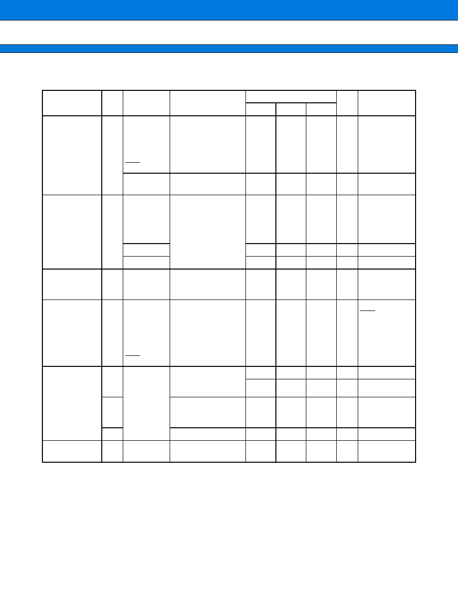
FUJITSU representatives beforehand.
5.5
5.0
4.0
3.0
2.0
1.0
0
1.0
2.0
3.0
4.0
5.0
6.0
7.0
8.0
9.0
10.0 11.0 12.0 13.0
4.0
2.0
0.8
0.4
0.33
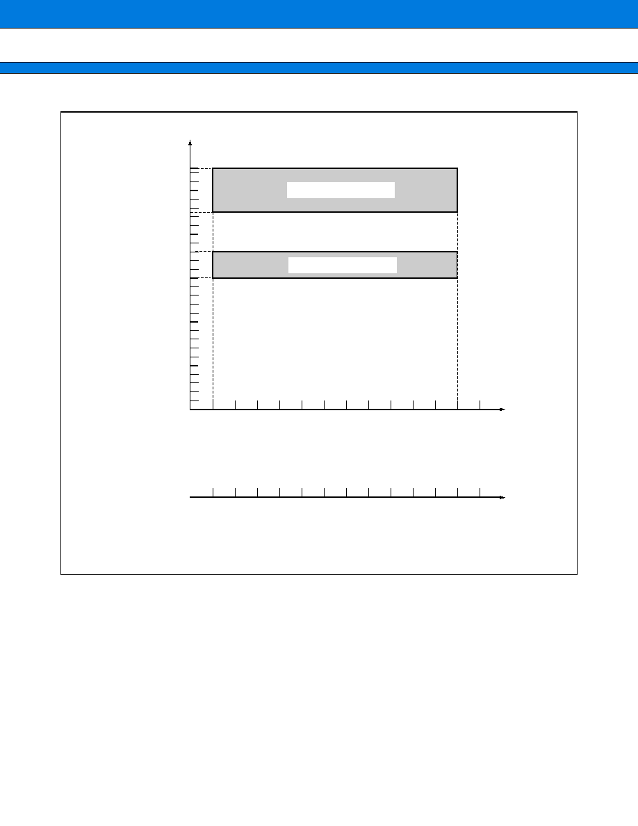
4.5
3.6
Guaranteed operation range
Guaranteed operation range
Operating voltage V
CC
(V)
CPU operating frequency (F
CH
MHz)
(At instruction cycle 4/ F
CH
)
Minimum execution time (instruction cycle) (
µ
s)
However, F
CH
= clock frequency (Fc)
×
2
·
Operating voltage vs. Operating frequency
MB89051 Series
27
3.
DC Characteristics (Power supply votage : 5.0 V)
(V
CC
=
5.0 V, V
SS
=
0 V, T
A
=
-
40
°
C to
+
85
°
C)
(Continued)
Parameter
Sym
bol
Pin
Condition
Value
Unit
Remarks
Min
Typ
Max
"H" level
Input voltage
V
IH
P00 to P07,
P10 to P17,
P20 to P27,
P40 to P47,
P53, P54,
MOD0,
MOD1,
MOD2
0.7 V
CC
V
CC
+
0.3
V
P31 to P37
2.5
3.3
V
3 V
V
IHS
RST,
UCK, UI
0.8 V
CC
V
CC
+
0.3
V
INT1 to INT7,
SCK1, SCK2,
SI1, SI2
2.9
3.3
V
3 V
V
IHI2C
SCL, SDA
0.8 V
CC
V
CC
+
5.5
V
"L" level
Input voltage
V
IL
P00 to P07,
P10 to P17,
P20 to P27,
P40 to P47,
P53, P54,
MOD0,
MOD1,
MOD2
V
SS
-
0.3
0.3 V
CC
V
P31 to P37
V
SS
-
0.3
0.9
3 V
V
ILS
RST,
INT1 to INT7,
UCK, UI
V
SS
-
0.3
0.2 V
CC
V
INT1 to INT7,
SCK1, SCK2,
SI1, SI2
V
SS
-
0.3
0.6
3 V
V
ILI2C
SCL, SDA
V
SS
-
0.3
0.3 V
CC
V
Open-drain out-
put application
voltage
V
D1
P53, P54
V
SS
-
0.3
V
CC
+
0.3
V
"H" level
Output voltage
V
OH
P00 to P07,
P10 to P17,
P20 to P24,
P40 to P47
I
OH
=
-
2.0 mA
4.0
V
P31 to P37,
CLK1, CLK2
I
OH
=
-
1.0 mA
2.6
3.6 V
V
3 V
USBP
I
OH
=
-
2.4 mA
3.0
3.6 V
V
USB Pull up
MB89051 Series
28
(Continued)
(V
CC
=
5.0 V, V
SS
=
0 V, T
A
=
-
40
°
C to
+
85
°
C)
Parameter
Sym
bol
Pin
Condition
Value
Unit
Remarks
Min
Typ
Max
"L" level
Output voltage
V
OL
P00 to P07,
P10 to P17,
P20 to P24,
P40 to P47,
P53, P54,
RST
I
OL
=
4.0 mA
0.4
V
P31 to P37,
CLK1, CLK2
I
OL
=
1.0 mA
0.4
V
3 V
Input leakage
current
(Hi-Z output
leakage current)
I
LI
P00 to P07,
P10 to P17,
P20 to P27,
P31 to P37,
P40 to P47,
0.0 V
<
V
I
<
V
CC
-
5
+
5
µ
A
When no pullup
re sistance is
speci fied
CLK1, CLK2
-
5
+
5
µ
A
USBP
-
5
+
5
µ
A
Open-drain out-
put leakage cur-
rent
I
LIOD
P53, P54
0.0 V
<
V
I
<
V
SS
+
5.5 V
+
5
µ
A
Pullup
resistance
R
PULL
P00 to P07,
P10 to P17,
P20 to P27,
P31 to P37,
P40 to P47,
P53, P54,
RST
V
I
=
0.0 V
25
50
100
k
RST is excluded
when pullup
resistance
available is
specified.
Power supply
current
I
CC
V
CC
F
CH
=
12.0 MHz,
V
CC
=
5.0 V,
t
inst
=
0.333
µ
s
29
42
mA
MB89F051
28
41
mA
MB89051
I
CCS1
F
CH
=
12.0 MHz,
V
CC
=
5.0 V,
t
inst
=
0.333
µ
s
20
30
mA
Sleep mode
I
CCH
T
A
=
+
25
°
C
40
70
µ
A
Stop
Input
capacitance
C
IN
Other than
V
CC
, V
SS
and
C
f
=
1 MHz
5
15
pF
MB89051 Series
29
4.
DC Characteristics (Power supply votage : 3.3 V)
(V
CC
=
3.3 V, V
SS
=
0 V, T
A
=
-
40
°
C to
+
85
°
C)
(Continued)
Parameter
Sym
bol
Pin
Condition
Value
Unit
Remarks
Min
Typ
Max
"H" level
Input voltage
V
IH
P00 to P07,
P10 to P17,
P20 to P27,
P31 to P37,
P40 to P47,
P53, P54,
MOD0, MOD1,
MOD2
0.7 V
CC
V
CC
+
0.3
V
V
IHS
RST,
UCK, UI,
INT1 to INT7,
SCK1, SCK2,
SI1, SI2
0.8 V
CC
V
CC
+
0.3
V
V
IHI2C
SCL, SDA
0.8 V
CC
V
CC
+
5.5
V
"L" level
Input voltage
V
IL
P00 to P07,
P10 to P17,
P20 to P27,
P31 to P37,
P40 to P47,
P53, P54,
MOD0, MOD1,
MOD2
V
SS
-
0.3
0.3 V
CC
V
V
ILS
RST,
INT1 to INT7,
UCK, UI,
INT1 to INT7,
SCK1, SCK2,
SI1, SI2
V
SS
-
0.3
0.2 V
CC
V
V
ILI2C
SCL, SDA
V
SS
-
0.3
0.3 V
CC
V
Open-drain
output application
voltage
V
D1
P53, P54
V
SS
-
0.3
V
CC
+
0.3
V
"H" level
Output voltage
V
OH
P00 to P07,
P10 to P17,
P20 to P24,
P40 to P47
I
OH
=
-
2.0 mA
2.6
V
P31 to P37,
CLK1, CLK2
I
OH
=
-
1.0 mA
2.6
V
USBP
I
OH
=
-
2.4 mA
3.0
V
USB Pull up,
Vcc
=
3.1 V to
3.6 V
MB89051 Series
30
(Continued)
(V
CC
=
3.3 V, V
SS
=
0 V, T
A
=
-
40
°
C to
+
85
°
C)
Parameter
Sym
bol
Pin
Condition
Value
Unit
Remarks
Min
Typ
Max
"L" level
Output voltage
V
OL
P00 to P07,
P10 to P17,
P20 to P24,
P40 to P47,
P53, P54,
RST
I
OL
=
4.0 mA
0.4
V
P31 to P37,
CLK1, CLK2
I
OL
=
1.0 mA
0.4
V
Input leakage
current
(Hi-Z output
leakage current)
I
LI
P00 to P07,
P10 to P17,
P20 to P27,
P31 to P37,
P40 to P47,
0.0 V
<
V
I
<
V
CC
-
5
+
5
µ
A
When no pullup
resistance is
specified
CLK1, CLK2
-
5
+
5
µ
A
USBP
-
5
+
5
µ
A
Open-drain
output leakage
current
I
LIOD
P53, P54
0.0 V
<
V
I
<
V
SS
+
5.5 V
+
5
µ
A
Pullup
resistance
R
PULL
P00 to P07,
P10 to P17,
P20 to P27,
P31 to P37,
P40 to P47,
P53, P54,
RST
V
I
=
0.0 V
25
50
100
k
RST is excluded
when pullup
resistance
available is
specified.
Power supply
current
I
CC
V
CC
F
CH
=
12.0 MHz,
V
CC
=
3.3 V,
t
inst
=
0.333
µ
s
29
42
mA
MB89F051
28
41
mA
MB89051
I
CCS1
F
CH
=
12.0 MHz,
V
CC
=
3.3 V,
t
inst
=
0.333
µ
s
20
30
mA
Sleep mode
I
CCH
T
A
=
+
25
°
C
40
70
µ
A
Stop
Input
capacitance
C
IN
Other than
Vcc and Vss
f
=
1 MHz
10
pF
MB89051 Series
31
5.
AC Characteristics
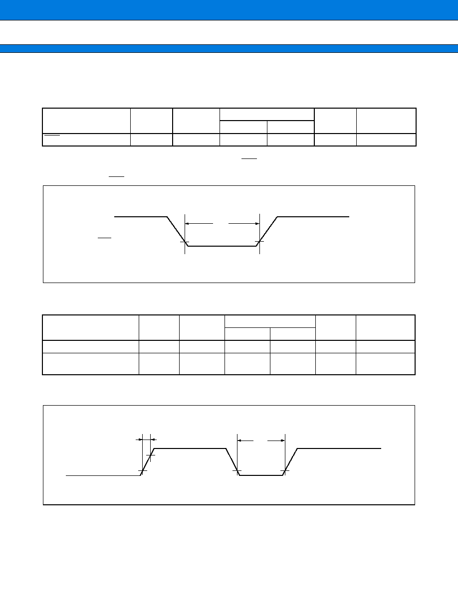
(1) Reset Timing
(V
CC
=
5.0 V, V
SS
=
0 V, T
A
=
-
40
°
C to
+
85
°
C)
Notes :
·
t
HCYL
is the oscillation cycle for the internal main clock.
·
If the reset pulse applied to the external reset pin (RST) does not meet the specifications, it may cause
malfunctions. Use caution so that the reset pulse less than the specifications will not be fed to the external
reset pin (RST).
(2) Power-on reset
(V
SS
=
0 V, T
A
=
-
40
°
C to
+
85
°
C)
Note : The power supply must be up within the selected oscillation stabilization time.
When the supply voltage needs to be varied while operating, it is recommended to smoothly start up the
voltage.
Parameter
Symbol
Condition
Value
Unit
Remarks
Min
Max
RST "L" pulse width
t
ZLZH
48 t
HCYL
ns
Parameter
Symbol
Condition
Value
Unit
Remarks
Min
Max
Power supply rising time
t
R
0.066
50
ms
Power supply cutoff time
t
OFF
4
ns
Due to repeated
operations
RST
0.2 V
CC
0.2 V
CC
t
ZLZH
V
CC
t
R
3.5 V
0.2 V
0.2 V
0.2 V
t
OFF
MB89051 Series
32
(3) Clock Timing
(V
SS
=
0 V, T
A
=
-
40
°
C to
+
85
°
C)
(4) Instruction Cycle
(V
SS
=
0 V, T
A
=
-
40
°
C to
+
85
°
C)
Parameter
Symbol Pin name Condition
Value
Unit
Remarks
Min
Typ
Max
Clock frequency
F
C
X0, X1
6
MHz
Clock cycle time
t
XCYL
X0, X1
166.6
ns
Internal main clock
frequency
F
CH
12
MHz
Twice the
Fc
Internal clock cycle
t
HCYL
83.3
ns
t
XCYL
/2
Parameter
Symbol
Value
Unit
Remarks
Instruction cycle
(Min execution time)
t
inst
4
/
F
CH
, 8
/
F
CH
,
16
/
F
CH
, 64
/
F
CH
µ
s
When operating at F
CH
= 12 MHz
t
inst
= 0.33
µ
s (4
/
F
CH
)
·
X0 and X1 Timing and Conditions
·
Clock Conditions
t
XCYL
0.2 V
CC
0.2 V
CC
X0
X0
C
1
C
2
X1
When a crystal resonator is used
MB89051 Series
33
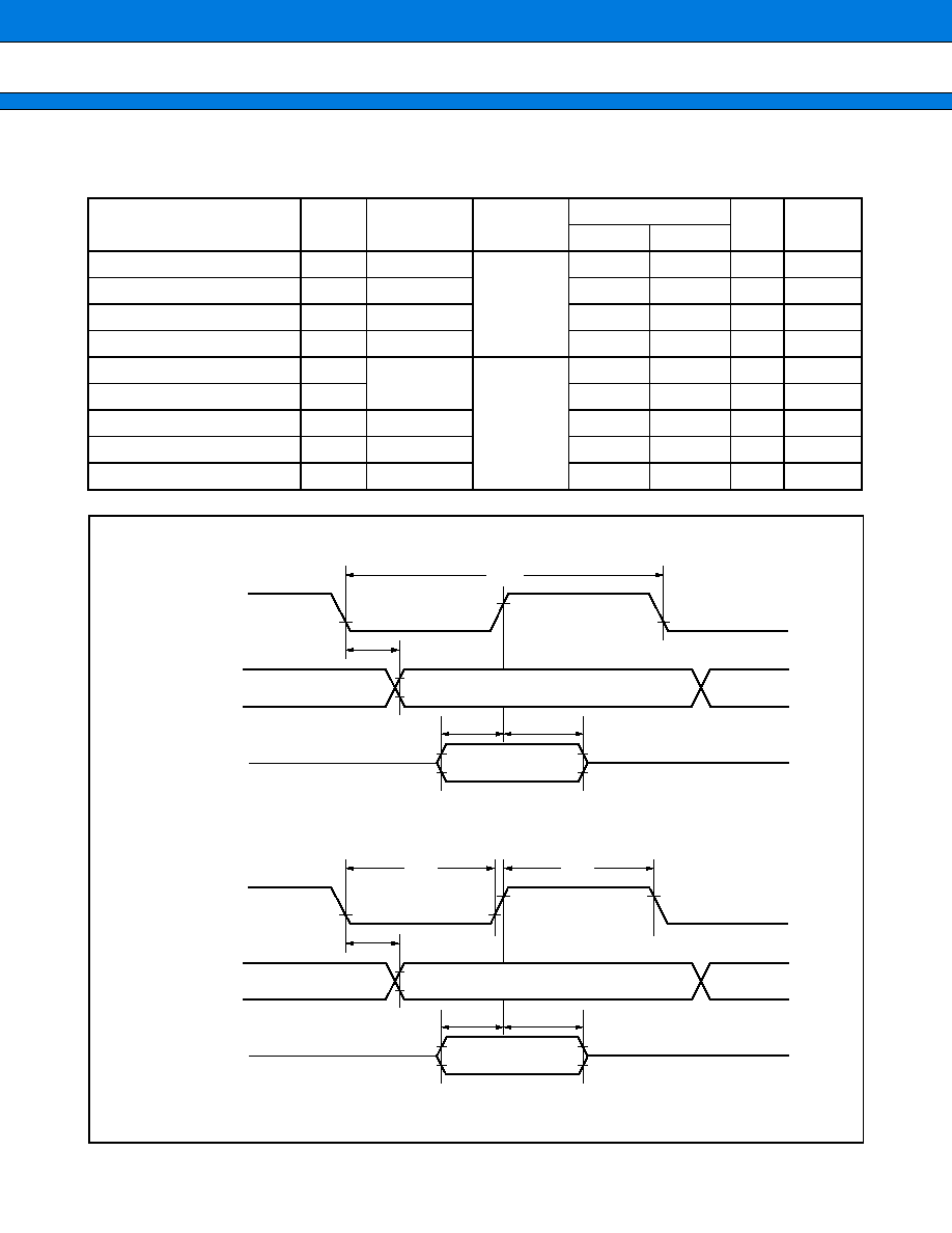
(5) UART Serial I/O Timing
(V
CC
=
5.0 V, V
SS
=
0 V, T
A
=
-
40
°
C to
+
85
°
C)
* : For information on t
inst
, see " (4) Instruction Cycle".
Parameter
Symbol
Pin name
Condition
Value
Unit
Remarks
Min
Max
Serial clock cycle time
t
SCYC
UCK
Internal shift
clock mode
2 t
inst
*
µ
s
UCK
UO
t
SLOV
UCK, UO
-
200
+
200
ns
Valid UI
UCK
t
IVSH
UI, UCK
200
ns
UCK
valid UI hold time
t
SHIX
UCK, UI
200
ns
Serial clock "H" pulse width
t
SHSL
UCK
External
shift clock
mode
1 t
inst
*
µ
s
Serial clock "L" pulse width
t
SLSH
1 t
inst
*
µ
s
UCK
UO time
t
SLOV
UCK, UO
0
200
ns
Valid UI
UCK
t
IVSH
UI, UCK
200
ns
UCK
valid UI hold time
t
SHIX
UCK, UI
200
ns
·
Internal shift clock mode
·
External shift clock mode
UCK
UO
UI
t
SCYC
t
IVSH
t
SLOV
t
SHIX
0.2 Vcc
0.2 Vcc
0.8 Vcc
0.8 V
CC
0.2 V
CC
0.8 V
CC
0.2 V
CC
0.2 Vcc
0.8 Vcc
UCK
UO
UI
t
SLSH
t
SHSL
t
IVSH
t
SLOV
t
SHIX
0.2 V
CC
0.2 Vcc
0.8 Vcc
0.8 V
CC
0.2 V
CC
0.8 V
CC
0.2 V
CC
0.2 V
CC
0.8 V
CC
0.8 V
CC
MB89051 Series
34
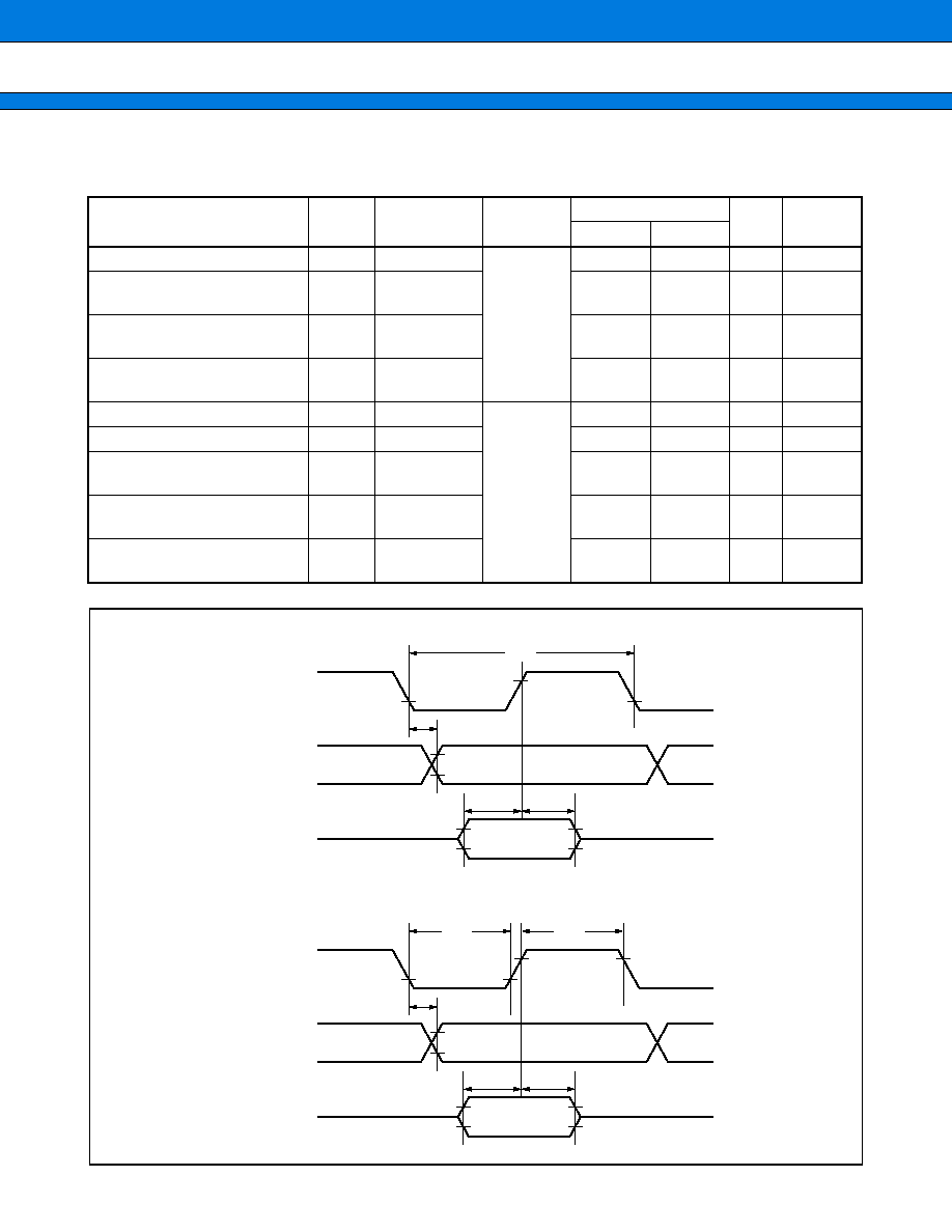
(6) Serial I/O Timing
(V
CC
=
5.0 V, Vss
=
0V, T
A
=
-
40
°
C to
+
85
°
C)
* : For information on t
inst
, see " (4) Instruction Cycle".
Parameter
Symbol
Pin name
Condition
Value
Unit
Remarks
Min
Max
Serial clock cycle time
t
SCYC
SCK1, SCK2
Internal
shift clock
mode
2 t
inst
*
µ
s
SCK
SO time
t
SLOV
SCK1, SO1,
SCK2, SO2
-
200
+
200
ns
Valid SI
SCK
t
IVSH
SCK1, SI1,
SCK2, SI2
200
ns
SCK
Valid SI hold time
t
SHIX
SCK1, SI1,
SCK2, SI2
200
ns
Serial clock "H" pulse width
t
SHSL
SCK1, SCK2
External
shift clock
mode
t
inst
*
µ
s
Serial clock "L" pulse width
t
SLSH
SCK1, SCK2
t
inst
*
µ
s
SCK
SO time
t
SLOV
SCK1, SO1,
SCK2, SO2
0
200
ns
Valid SI
SCK
t
IVSH
SCK1, SI1,
SCK2, SI2
200
µ
s
SCK
Valid SI hold time
t
SHIX
SCK1, SI1,
SCK2, SI2
200
µ
s
·
Internal shift clock mode
·
External shift clock mode
0.6
2.9
2.9
2.9
0.6
0.6
t
SCYC
t
SLOV
t
IVSH
t
SHIX
SCK1
SCK2
SO1
SO2
SI1
SI2
0.6
2.9
0.6
0.6
0.6
2.9
2.9
2.9
2.9
0.6
t
SLSH
t
SHSL
t
SLOV
t
IVSH
t
SHIX
SCK1
SCK2
SO1
SO2
SI1
SI2
0.6
2.9
0.6
MB89051 Series
35
(7) Peripheral Input Timing
(V
CC
=
5.0 V, V
SS
=
0 V, T
A
=
-
40
°
C to
+
85
°
C)
* : For information on t
inst
, see " (4) Instruction Cycle".
Parameter
Symbol
Pin name
Condition
Value
Unit
Remarks
Min
Max
Peripheral input "H" pulse
width 1
t
ILIH1
INT1 to INT7
2 t
inst
*
µ
s
Peripheral input "L" pulse
width 1
t
IHIL1
2 t
inst
*
µ
s
INT1 ~ INT7
t
IHIL1
t
ILIH1
0.6
0.6
0.8 V
CC
2.9
MB89051 Series
36
(8) I
2
C Timing
(V
CC
=
5.0 V, V
SS
=
0 V, T
A
=
-
40
°
C to
+
85
°
C)
*1 : For information on t
inst
, see " (4) Instruction Cycle".
*2 : m is defined in the ICCR CS 4 to CS 3 (bit 4 to bit 3) .
*3 : n is defined in the ICCR CS 2 to CS 0 (bit 2 to bit 0) .
Parameter
Sym
bol
Pin
Value
Unit
Remarks
Min
Max
Start condition output
t
STA
SCL,
SDA
1
/
4
×
t
inst
*
1
×
m
t
*
×
n
t
*
3
-
20
1
/
4
×
t
inst
*
1
×
m
t
*
2
×
n
t
*
3
+
20
ns
Master
mode
Stop condition output
t
STO
SCL,
SDA
1
/
4
×
t
inst
*
1
×
(m
t
*
2
×
n
t
*
3
+
8)
-
20
1
/
4
×
t
inst
*
1
×
(m
t
*
2
×
n
t
*
3
+
8)
+
20
ns
Master
mode
Start condition detect
t
STA
SCL,
SDA
1
/
4
×
t
inst
*
1
×
6
+
40
ns
Stop condition detect
t
STO
SCL,
SDA
1
/
4
×
t
inst
*
1
×
6
+
40
ns
Restart condition output t
STASU
SCL,
SDA
1
/
4
×
t
inst
*
1
×
(m
t
*
2
×
n
t
*
3
+
8)
-
20
1
/
4
×
t
inst
*
1
×
(m
t
*
2
×
n
t
*
3
+
8)
+
20
ns
Master
mode
Restart condition detect t
STASU
SCL,
SDA
1
/
4
×
t
inst
*
1
×
4
+
40
ns
SCL output Low width
t
LOW
SCL
1
/
4
×
t
inst
*
1
×
m
t
*
2
×
n
t
*
3
-
20
1
/
4
×
t
inst
*
1
×
m
t
*
2
×
n
t
*
3
+
20
ns
Master
mode
SCL output High width
t
HIGH
SCL
1
/
4
×
t
inst
*
1
×
(m
t
*
2
×
n
t
*
3
+
8)
-
20
1
/
4
×
t
inst
*
1
×
(m
t
*
2
×
n
t
*
3
+
8)
+
20
ns
Master
mode
SDA output delay
t
DO
SDA
1
/
4
×
t
inst
*
1
×
4
-
20
1
/
4
×
t
inst
*
1
×
4
+
20
ns
SDA output setup time
after interrupt
t
DOSU
SDA
1
/
4
×
t
inst
*
1
×
4
-
20
ns
SCL input Low pulse
width
t
LOW
SCL
1
/
4
×
t
inst
*
1
×
6
+
40
ns
SCL input High pulse
width
t
HIGH
SCL
1
/
4
×
t
inst
*
1
×
2
+
40
ns
SDA input setup time
t
SU
SDA
40
ns
SDA hold time
t
HO
SDA
0
ns
Data transmit (master/slave)
Data receive (master/slave)
9
ACK
t
DO
t
SU
t
SU
t
DOSU
t
DO
t
HO
t
LOW
t
STA
SDA
SCL
1
t
STASU
SDA
SCL
6
7
8
9
t
SU
t
HIGH
t
LOW
t
HO
t
DO
t
DO
t
DOSU
t
STO
ACK
MB89051 Series
37
6.
FLASH Program/Erase characteristics
·
·
·
·
Program/Erase characteristics
Parameter
Condition
Value
Unit
Remarks
Min
Typ
Max
Sector erase time
T
A
=
+
25
°
C
Vcc
=
5.0 V
1
15
s
Except for the write time before internal
erase operation
Chip erase time
5
75
s
Except for the write time before internal
erase operation
Byte program time
8
3,600
µ
s
Except for the over head time of the system.
Prgram/erase cycle
10,000
cycle

MB89051 Series
38
s
ORDERING INFORMATION
Part Number
Package
Remarks
MB89051PFM
MB89F051PFM
64-pin plastic LQFP
(FPT-64P-M09)
MB89051 Series
39
s
PACKAGE DIMENSIONS
64-pin plastic LQFP
(FPT-64P-M09)
Note 1) * : These dimensions do not include resin protrusion.
Note 2) Pins width and pins thickness include plating thickness.
Note 3) Pins width do not include tie bar cutting remainder.
Dimensions in mm (inches)
Note : The values in parentheses are reference values.
C
2003 FUJITSU LIMITED F64018S-c-3-5
0.65(.026)
0.10(.004)
1
16
17
32
49
64
33
48
12.00±0.10(.472±.004)SQ
14.00±0.20(.551±.008)SQ
INDEX
0.32±0.05
(.013±.002)
M
0.13(.005)
0.145±0.055
(.0057±.0022)
"A"
.059
.004
+.008
0.10
+0.20
1.50
0~8°
0.25(.010)
(Mounting height)
0.50±0.20
(.020±.008)
0.60±0.15
(.024±.006)
0.10±0.10
(.004±.004)
Details of "A" part
(Stand off)
0.10(.004)
*

MB89051 Series
FUJITSU LIMITED
All Rights Reserved.
The contents of this document are subject to change without notice.
Customers are advised to consult with FUJITSU sales
representatives before ordering.
The information, such as descriptions of function and application
circuit examples, in this document are presented solely for the
purpose of reference to show examples of operations and uses of
Fujitsu semiconductor device; Fujitsu does not warrant proper
operation of the device with respect to use based on such
information. When you develop equipment incorporating the
device based on such information, you must assume any
responsibility arising out of such use of the information. Fujitsu
assumes no liability for any damages whatsoever arising out of
the use of the information.
Any information in this document, including descriptions of
function and schematic diagrams, shall not be construed as license
of the use or exercise of any intellectual property right, such as
patent right or copyright, or any other right of Fujitsu or any third
party or does Fujitsu warrant non-infringement of any third-party's
intellectual property right or other right by using such information.
Fujitsu assumes no liability for any infringement of the intellectual
property rights or other rights of third parties which would result
from the use of information contained herein.
The products described in this document are designed, developed
and manufactured as contemplated for general use, including
without limitation, ordinary industrial use, general office use,
personal use, and household use, but are not designed, developed
and manufactured as contemplated (1) for use accompanying fatal
risks or dangers that, unless extremely high safety is secured, could
have a serious effect to the public, and could lead directly to death,
personal injury, severe physical damage or other loss (i.e., nuclear
reaction control in nuclear facility, aircraft flight control, air traffic
control, mass transport control, medical life support system, missile
launch control in weapon system), or (2) for use requiring
extremely high reliability (i.e., submersible repeater and artificial
satellite).
Please note that Fujitsu will not be liable against you and/or any
third party for any claims or damages arising in connection with
above-mentioned uses of the products.
Any semiconductor devices have an inherent chance of failure. You
must protect against injury, damage or loss from such failures by
incorporating safety design measures into your facility and
equipment such as redundancy, fire protection, and prevention of
over-current levels and other abnormal operating conditions.
If any products described in this document represent goods or
technologies subject to certain restrictions on export under the
Foreign Exchange and Foreign Trade Law of Japan, the prior
authorization by Japanese government will be required for export
of those products from Japan.
F0303
©
FUJITSU LIMITED Printed in Japan
Document Outline