Äîêóìåíòàöèÿ è îïèñàíèÿ www.docs.chipfind.ru
REV. A
Information furnished by Analog Devices is believed to be accurate and
reliable. However, no responsibility is assumed by Analog Devices for its
use, nor for any infringements of patents or other rights of third parties
which may result from its use. No license is granted by implication or
otherwise under any patent or patent rights of Analog Devices.
a
ADP3820
One Technology Way, P.O. Box 9106, Norwood, MA 02062-9106, U.S.A.
Tel: 781/329-4700
World Wide Web Site: http://www.analog.com
Fax: 781/326-8703
© Analog Devices, Inc., 1999
Lithium-Ion
Battery Charger
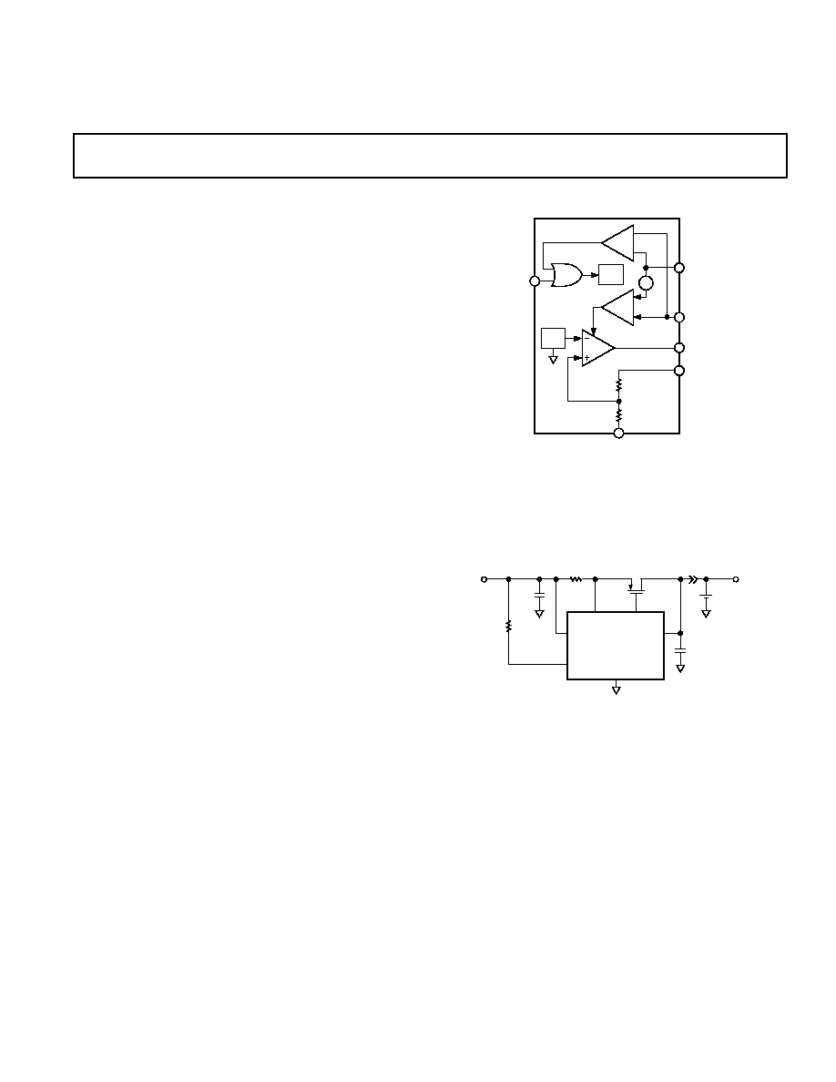
FUNCTIONAL BLOCK DIAGRAM
V
IN
IS
GATE
V
OUT
SD
50mV
+
BIAS
V
REF
ADP3820
GND
FEATURES
1% Total Accuracy
630 A Typical Quiescent Current
Shutdown Current: 1 A (Typical)
Stable with 10 F Load Capacitor
4.5 V to 15 V Input Operating Range
Integrated Reverse Leakage Protection
6-Lead SOT-23-6 and 8-Lead SO-8 Packages
Programmable Charge Current
20 C to +85 C Ambient Temperature Range
Internal Gate-to-Source Protective Clamp
APPLICATIONS
Li-Ion Battery Chargers
Desktop Computers
Hand-Held Instruments
Cellular Telephones
Battery Operated Devices
GENERAL DESCRIPTION
The ADP3820 is a precision single cell Li-Ion battery charge
controller that can be used with an external Power PMOS de-
vice to form a two-chip, low cost, low dropout linear battery
charger. It is available in two voltage options to accommodate
Li-Ion batteries with coke or graphite anodes. The ADP3820's
high accuracy (
±
1%) low shutdown current (1
µ
A) and easy
charge current programming make this device especially attrac-
tive as a battery charge controller.
Charge current can be set by an external resistor. For example,
50 m
of resistance can be used to set the charge current to
1 A. Additional features of this device include foldback current
limit, overload recovery, and a gate-to-source voltage clamp to
protect the external MOSFET. The proprietary circuit also
minimizes the reverse leakage current from the battery if the
input voltage of the charger is disconnected. This feature elimi-
nates the need for an external serial blocking diode.
The ADP3820 operates with a wide input voltage range from
4.5 V to 15 V. It is specified over the industrial temperature
range of 20
°
C to +85
°
C and is available in the ultrasmall
6-lead surface mount SOT-23-6 and 8-lead SOIC packages.
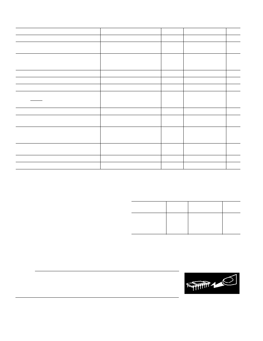
C1
10 F
+
R1
10k
V
IN
+5V
R
S
50m
22 F
V
OUT
Li-Ion
BATTERY
I
O
= 1A
NDP6020P
GND
IS
GATE
V
IN
SD
V
OUT
ADP3820-xx
Figure 1. Li-Ion Charger Application Circuit
2
REV. A
ADP3820SPECIFICATIONS
1
Parameter
Conditions
Symbol
Min
Typ
Max
Units
INPUT VOLTAGE
V
IN
4.5
15
V
OUTPUT VOLTAGE ACCURACY
V
IN
= V
OUT
+ 1 V to 15 V
V
OUT
1
+1
%
V
SD
= 2 V
QUIESCENT CURRENT
Shutdown Mode
V
SD
= 0 V
I
GND
1
15
µ
A
Normal Mode
V
SD
= 2 V
I
GND
630
800
µ
A
GATE TO SOURCE CLAMP VOLTAGE
6
10
V
GATE DRIVE MINIMUM VOLTAGE
2
0.7
V
GATE DRIVE CURRENT (SINK/SOURCE)
1
mA
GAIN
V
V
GS
OUT
80
dB
CURRENT LIMIT THRESHOLD VOLTAGE
V
IN
V
IS
40
75
mV
LOAD REGULATION
I
OUT
= 10 mA to 1 A,
Circuit of Figure 1
10
+10
mV
LINE REGULATION
V
IN
= V
OUT
+ 1 V to 15 V
I
OUT
= 0.1 A
Circuit of Figure 1 (No Battery)
10
+10
mV
SD INPUT VOLTAGE
V
IH
V
SD
2.0
V
V
IL
0.4
V
SD INPUT CURRENT
V
SD
= 0 V to 5 V
I
SD
15
+15
µ
A
OUTPUT REVERSE LEAKAGE CURRENT
V
IN
= Floating
I
DISCH
3
5
µ
A
NOTES
1
All limits at temperature extremes are guaranteed via correlation using standard Statistical Quality Control (SQC).
2
Provided gate-to-source clamp voltage is not exceeded.
Specifications subject to change without notice.
CAUTION
ESD (electrostatic discharge) sensitive device. Electrostatic charges as high as 4000 V readily
accumulate on the human body and test equipment and can discharge without detection.
Although the ADP3820 features proprietary ESD protection circuitry, permanent damage may
occur on devices subjected to high energy electrostatic discharges. Therefore, proper ESD
precautions are recommended to avoid performance degradation or loss of functionality.
WARNING!
ESD SENSITIVE DEVICE
ABSOLUTE MAXIMUM RATINGS*
Input Voltage, V
IN
. . . . . . . . . . . . . . . . . . . . . . . . . . . .
20 V
Enable Input Voltage . . . . . . . . . . . . . . . 0.3 V to (V
IN
+ 0.3 V)
Operating Ambient Temperature Range . . . . 20
°
C to +85
°
C
Storage Temperature Range . . . . . . . . . . . . 65
°
C to +150
°
C
JA
, SO-8 Package . . . . . . . . . . . . . . . . . . . . . . . . 150
°
C/W
JA
, SOT-23-6 Package . . . . . . . . . . . . . . . . . . . . 230
°
C/W
Lead Temperature (Soldering, 10 sec) . . . . . . . . . . . . +300
°
C
Vapor Phase (60 sec) . . . . . . . . . . . . . . . . . . . . . . . . +215
°
C
Infrared (15 sec) . . . . . . . . . . . . . . . . . . . . . . . . . . .+220
°
C
ESD Rating . . . . . . . . . . . . . . . . . . . . . . . . . . . . . . . . . . . 2 kV
*This is a stress rating only; operation beyond these limits can cause the device
to be permanently damaged.
ORDERING GUIDE
Voltage
Package
Marking
Model
Output
Option*
Code
ADP3820ART-4.1
4.1 V
RT-6 (SOT-23-6) BAC
ADP3820ART-4.2
4.2 V
RT-6 (SOT-23-6) BBC
ADP3820AR-4.1
4.1 V
SO-8
ADP3820AR-4.2
4.2 V
SO-8
*SOT = Surface Mount Package. SO = Small Outline.
Contact the factory for availability of other output voltage options.
(V
IN
= [V
OUT
+ 1 V] T
A
= 20 C to +85 C, unless otherwise noted)
ADP3820
3
REV. A
PIN FUNCTION DESCRIPTIONS
Pin
Pin
SOT-23-6 SO-8
Name
Function
1
8
SD
Shutdown. Pulling this pin low
will disable the output.
2
7
GND
Device Ground. This pin should
be tied to system ground closest
to the load.
3
5
V
OUT
Output Voltage Sense. This pin
is connected to the MOSFET's
drain and directly to the load for
optimal load regulation. Bypass
to ground with a 10
µ
F or larger
capacitor.
4
3
GATE
Gate drive for the external
MOSFET.
5
4
V
IN
Input Voltage. This is also the
positive terminal connection of
the current sense resistor.
6
1
IS
Current Sense. Used to sense the
input current by monitoring the
voltage across the current sense
resistor. It is connected to the
more negative terminal of the
resistor as well as the power
MOSFET's source pin. IS pin
should be tied to the V
IN
pin if
the current limit feature is not
used.
2, 6
NC
No Connect.
PIN CONFIGURATIONS
SO-8
RT-6 (SOT-23-6)
TOP VIEW
(Not to Scale)
8
7
6
5
1
2
3
4
NC = NO CONNECT
IS
NC
GATE
V
IN
SD
GND
NC
V
OUT
ADP3820
TOP VIEW
(Not to Scale)
6
5
4
1
2
3
SD
GND
V
OUT
IS
V
IN
GATE
ADP3820
ADP3820
4
REV. A
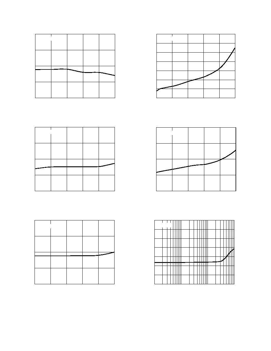
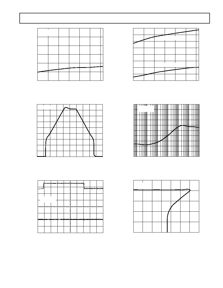
Typical Performance Characteristics
I
LOAD
mA
4.110
4.105
4.090
0
1000
200
OUTPUT VOLTAGE V
400
600
800
4.100
4.095
V
IN
= 5.1V
Figure 2. V
OUT
vs. I
LOAD
(V
IN
= 5.1 V)*
4.110
4.105
4.090
5
15
7
OUTPUT VOLTAGE V
9
11
13
4.100
4.095
INPUT VOLTAGE V
I
LOAD
= 1A
Figure 3. V
OUT
vs. V
IN
(I
LOAD
= 1 A)*
4.110
4.105
4.090
5
15
7
OUTPUT VOLTAGE V
9
11
13
4.100
4.095
INPUT VOLTAGE V
I
LOAD
= 10mA
Figure 4. V
OUT
vs. V
IN
(I
LOAD
= 10 mA)*
INPUT VOLTAGE V
0.760
0.740
0.680
5
15
7
I
GND
mA
9
11
13
0.720
0.700
0.660
0.640
0.620
I
LOAD
= 10mA
Figure 5. I
GND
vs. V
IN
(I
LOAD
= 10 mA)*
INPUT VOLTAGE V
0.900
0.850
0.700
5
15
7
I
GND
mA
11
13
0.800
0.750
I
LOAD
= 1A
9
Figure 6. I
GND
vs. V
IN
(I
LOAD
= 1 A)*
I
LOAD
mA
1.200
0.500
0.001
1000
I
GND
mA
1.100
10
0.1
1.000
0.900
0.800
0.700
0.600
V
IN
= 5.1V
Figure 7. I
GND
vs. I
LOAD
(V
IN
= 5.1 V)*
*Reference Figure 1.
ADP3820
5
REV. A
TEMPERATURE C
1.100
0.500
40
80
20
I
GND
mA
0
20
40
60
1.000
0.900
0.800
0.700
0.600
V
IN
= 5.1V
I
LOAD
= 10mA
Figure 8. Quiescent Current vs. Temperature*
INPUT VOLTAGE V
0
0
1
2
3
4
5
4
3
2
1
4.5
4.0
0
OUTPUT VOLTAGE V
2.0
1.5
1.0
0.5
3.0
2.5
3.5
I
LOAD
= 10mA
Figure 9. Power-Up/Power-Down*
4.2
4.1
4.0
5.5
7.0
I
LOAD
= 10mA
C
OUT
= 10 F
OUTPUT
VOLTAGE V
INPUT
VOLTAGE V
Figure 10. Line Transient Response (10
µ
F Output Cap)*
TEMPERATURE C
4.230
4.110
40
80
20
OUTPUT VOLTAGE V
0
20
40
60
4.210
4.190
4.170
4.150
4.130
4.090
4.070
V
OUT
= 4.2V
V
OUT
= 4.1V
Figure 11. V
OUT
vs. Temperature, V
IN
= 5.1 V, I
LOAD
= 10 mA*
FREQUENCY Hz
0
100
10
1M
PSRR dB
50
100
1k
10k
100k
10
20
30
40
60
70
80
90
10M
C
LOAD
= 10 F
I
LOAD
= 1mA
Figure 12. Ripple Rejection*
I
LOAD
mA
5.000
4.000
0.000
0
140
20
OUTPUT VOLTAGE V
40
60
80
100
120
3.000
2.000
V
IN
= 5.1V
R
S
= 0.5
1.000
Figure 13. Current Limit Foldback*

ADP3820
6
REV. A
APPLICATION INFORMATION
The ADP3820 is very easy to use. A P-channel power MOS-
FET and a small capacitor on the output is all that is needed to
form an inexpensive Li-Ion battery charger. The advantage of
using the ADP3820 controller is that it can directly drive a
PMOS FET to provide a regulated output current until the
battery is charged. When the specified battery voltage is reached,
the charge current is reduced and the ADP3820 maintains the
maximum specified battery voltage accurately.
When fully charged, the circuit in Figure 1 works like a well
known linear regulator, holding the output voltage within the
specified accuracy as needed by single cell Li-Ion batteries. The
output is sensed by the V
OUT
pin. When charging a discharged
battery, the circuit maintains a set charging current determined
by the current sense resistor until the battery is fully charged,
then reduces it to a trickle charge to keep the battery at the
specified voltage. The voltage drop across the R
S
current sense
resistor is sensed by the IS input of the ADP3820. At minimum
battery voltage or at shorted battery, the circuit reduces this
current (foldback) to limit the dissipation of the FET (see Fig-
ure 13). Both the V
IN
input and V
OUT
sense pins of the IC need
to be bypassed by a suitable bypass capacitor.
A 6 V gate-to-source voltage clamp is provided by the ADP3820
to protect the MOSFET gates at higher source voltages. The
ADP3820 also has a TTL
SD input, which may be connected to
the input voltage to enable the IC. Pulling it to low or to
ground will disable the FET-drive.
Design Approach
Due to the lower efficiency of Linear Regulator Charging, the
most important factor is the thermal design and cost, which is
the direct function of the input voltage, output current and
thermal impedance between the MOSFET and the ambient
cooling air. The worse-case situation is when the battery is
shorted since the MOSFET has to dissipate the maximum power.
A tradeoff must be made between the charge current, cost and
thermal requirements of the charger. Higher current requires a
larger FET with more effective heat dissipation leading to a
more expensive design. Lowering the charge current reduces
cost by lowering the size of the FET, possibly allowing a smaller
package such as SOT-23-6. The following designs consider both
options. Furthermore, each design is evaluated under two input
source voltage conditions.
Regarding input voltage, there are two options:
A. The input voltage is preregulated, e.g., 5 V
±
10%
B. The input voltage is not a preregulated source, e.g., a wall
plug-in transformer with a rectifier and capacitive filter.
Higher Current Option
A. Preregulated Input Voltage (5 V 10%)
For the circuit shown in Figure 1, the required
JA
thermal
impedance can be calculated as follows: if the FET data sheet
allows a max FET junction temperature of T
JMAX
= 150
°
C, then
at 50
°
C ambient and at convection cooling, the maximum al-
lowed
T junction temperature rise is thus, T
JMAX
T
AMAX
=
150
°
C 50
°
C = 100
°
C.
The maximum current for a shorted or discharged battery is
reduced from the set charge current by a multiplier factor shown
in Figure 13 due to the foldback current limiting feature of the
ADP3820. This k factor between V
O
of 0 V to about 2.5 V is:
k ~ 0.65.
JA
=
T/(I
O
×
k
×
V
IN
) = 100/(1
×
0.65
×
5) = 30.7
°
C/W
This thermal impedance can be realized using the transistor
shown in Figure 1 when surface mounted to a 40
×
40 mm
double-sided PCB with many vias around the tab of the surface-
mounted FET to the backplane of the PCB. Alternatively, a
TO-220 packaged FET mounted to a heatsink could be used.
The
or thermal impedance of a suitable heatsink is calculated
below:
< (
JA
JC
) = 30.7 2 = +28.7
°
C/W
Where the
JC
, or junction-to-case thermal impedance of the
FET can be read from the FET data sheet. A low cost such
heatsink is type PF430 made by Thermalloy, with a
=
+25.3
°
C/W.
The current sense resistor for this application can be simply
calculated:
R
S
= V
S
/I
O
= 0.05/1 = 50 m
Where V
S
is specified on the data sheet as current limit threshold
voltage at 40 mV75 mV. For battery charging applications, it
is adequate to use the typical 50 mV midvalue.
B. Nonpreregulated Input Voltage
If the input voltage source is, for example, a rectified and
capacitor-filtered secondary voltage of a small wall plug-in
transformer, the heatsinking requirement is more demanding.
The V
INMIN
should be specified 5 V, but at the lowest line volt-
age and full load current. The required thermal impedance can
be calculated the same way as above, but here we have to use
the maximum output rectified voltage, which can be substan-
tially higher than 5 V, depending on transformer regulation and
line voltage variation. For example, if V
INMAX
is 10 V
JA
=
T/(I
O
×
k
×
V
INMAX
) = 100/(1
×
0.65
×
10) = +15.3
°
C/W
The
suitable heatsink thermal impedance:
<
JA
JC
= 15.3 2 = 13.3
°
C/W
A low cost heatsink is Type 6030B made by Thermalloy, with a
= +12.5
°
C/W.
Lower Current Option
A. Preregulated Input Voltage (5 V 10%)
If lower charging current is allowed, the
JA
value can be increased,
and the system cost decreased. The lower cost is assured by
using an inexpensive MOSFET with, for example, a NDT452P
in a SOT-23-6 package mounted on a small 40
×
40 mm area
on double-sided PCB. This provides a convection cooled ther-
mal impedance of
JA
= +55
°
C/W, presuming many vias are
used around the FET to the backplane. Allowing a maximum
FET junction temperature of +150
°
C, at +50
°
C ambient, and
at convection cooling the maximum allowed heat rise is thus
150
°
C50
°
C = 100
°
C.
The maximum foldback current allowed:
I
FB
=
T/(
×
V
IN
) = 100/(55
×
5) = 0.33 A
Thus the full charging current:
I
OUTMAX
= I
FB
/k = 0.5 A
k is calculated in the above example.
ADP3820
7
REV. A
The current sense resistor for this application:
R
S
= V
S
/I
O
= 0.05/0.5 = 100 m
FET Selection
The type and size of the pass transistor are determined by the
threshold voltage, input-output voltage differential and load
current. The selected PMOS must satisfy the physical and ther-
mal design requirements. To ensure that the maximum V
GS
provided by the controller will turn on the FET at worst case
conditions, (i.e., temperature and manufacturing tolerances) the
maximum available V
GS
must be determined. Maximum V
GS
is
calculated as follows:
V
GS
= V
IN
V
BE
I
OUTMAX
×
R
S
where
I
OUTMAX
= Maximum Output Current
R
S
= Current Sense Resistor
V
BE
~ 0.7 V (Room Temperature)
~ 0.5 V (Hot)
~ 0.9 V (Cold)
For example:
V
IN
= 5 V, and I
OUTMAX
= 1 A,
V
GS
= 5 V 0.7 V 1 A
×
50 m
= 4.25 V
If V
GS
< 5 V, logic level FET should be considered.
If V
GS
> 5 V, either logic level or standard MOSFET can be
used.
The difference between V
IN
and V
O
(V
DS
) must exceed the
voltage drop due to the sense resistor plus the ON-resistance
of the FET at the maximum charge current. The selected
MOSFET must satisfy these criteria; otherwise, a different pass
device should be used.
V
DS
= V
IN
V
O
= 5 V 4.2 V = 0.8 V
The maximum R
DS(ON)
required at the available gate drive (V
DR
)
and Drain-to-Source voltage (V
DS
) is:
R
DS(ON)
= V
DS
/I
OUTMAX
From the Drain-to Source current vs. Drain-to-Source voltage
vs. gate drive graph off the MOSFET data sheet, it can be de-
termined if the above calculated R
DS(ON)
is higher than the graph
indicates. However, the value read from the MOSFET data
sheet graph must be adjusted based on the junction temperature
of the MOSFET. This adjustment factor can be obtained from
the normalized R
DS(ON)
vs. junction temperature graph in the
MOSFET data sheet.
External Capacitors
The ADP3820 is stable with or without a battery load, and
virtually any good quality output filter capacitors can be used
(anyCAPTM), independent of the capacitor's minimum ESR
(Effective Series Resistance) value. The actual value of the
capacitor and its associated ESR depends on the g
m
and capaci-
tance of the external PMOS device. A 10
µ
F tantalum or alumi-
num electrolytic capacitor at the output is sufficient to ensure
stability for up to a 10 A output current.
Shutdown Mode
Applying a TTL high signal to the
SD pin or tying it to the
input pin will enable the output. Pulling this pin low or tying
it to ground will disable the output. In shutdown mode, the
controller's quiescent current is reduced to less than 1
µ
A.
Gate-to-Source Clamp
A 6 V gate-to-source voltage clamp is provided by the ADP3820 to
protect most MOSFET gates in the event the V
IN
> V
GS
allowed
and the output is suddenly shorted to ground. This allows use of
the new, low R
DS(ON)
MOSFETs.
Short Circuit Protection
The power FET is protected during short circuit conditions
with a foldback type of current limiting that significantly re-
duces the current. See Figure 13 for foldback current limit
information.
Current Sense Resistor
Current limit is achieved by setting an appropriate current sense
resistor (R
S
) across the current limit threshold voltage. Current
limit sense resistor, R
S
, is calculated as shown above. Proper
derating is advised to select the power dissipation rating of the
resistor.
The simplest and cheapest sense resistor for high current appli-
cations, (i.e., Figure 1) is a PCB trace. However, the tempera-
ture dependence of the copper trace and the thickness tolerances of
the trace must be considered in the design. The resistivity of
copper has a positive temperature coefficient of +0.39%/
°
C.
Copper's Tempco, in conjunction with the proportional-to-
absolute temperature (
±
0.3%) current limit voltage, can provide
an accurate current limit. Table I provides the typical resistance
values for PCB copper traces. Alternately, an appropriate sense
resistor, such as surface mount sense resistors, available from
KRL, can be used.
Table I. Printed Circuit Copper Resistance
Conductor
Conductor
Resistance
Thickness
Width/Inch
m /In
1/2oz/ft
2
(18
µ
m)
0.025
39.3
0.050
19.7
0.100
9.83
0.200
4.91
0.500
1.97
1oz/ft
2
(35
µ
m)
0.025
19.7
0.050
9.83
0.100
4.91
0.200
2.46
0.500
0.98
2oz/ft
2
(70
µ
m)
0.025
9.83
0.050
4.91
0.100
2.46
0.200
1.23
0.500
0.49
3oz/ft
2
(106
µ
m)
0.025
6.5
0.050
3.25
0.100
1.63
0.200
0.81
0.500
0.325
anyCAP is a trademark of Analog Devices, Inc.
ADP3820
8
REV. A
C2986a29/99
PRINTED IN U.S.A.
6-Lead Plastic Surface Mount Package
RT-6 (SOT-23-6)
0.122 (3.10)
0.106 (2.70)
PIN 1
0.118 (3.00)
0.098 (2.50)
0.075 (1.90)
BSC
0.037 (0.95) BSC
1
3
4
5
6
2
0.071 (1.80)
0.059 (1.50)
0.009 (0.23)
0.003 (0.08)
0.022 (0.55)
0.014 (0.35)
10
0
0.020 (0.50)
0.010 (0.25)
0.006 (0.15)
0.000 (0.00)
0.051 (1.30)
0.035 (0.90)
SEATING
PLANE
0.057 (1.45)
0.035 (0.90)
8-Lead Narrow Body Package
SO-8
0.0098 (0.25)
0.0075 (0.19)
0.0500 (1.27)
0.0160 (0.41)
8
0
0.0196 (0.50)
0.0099 (0.25)
45
8
5
4
1
0.1968 (5.00)
0.1890 (4.80)
0.2440 (6.20)
0.2284 (5.80)
PIN 1
0.1574 (4.00)
0.1497 (3.80)
0.0500 (1.27)
BSC
0.0688 (1.75)
0.0532 (1.35)
SEATING
PLANE
0.0098 (0.25)
0.0040 (0.10)
0.0192 (0.49)
0.0138 (0.35)
PCB Layout Issues
For optimum voltage regulation, place the load as close as pos-
sible to the device's V
OUT
and GND pins. It is recommended to
use dedicated PCB traces to connect the MOSFET's drain to
the positive terminal and GND to the negative terminal of the
load to avoid voltage drops along the high current carrying PCB
traces.
OUTLINE DIMENSIONS
Dimensions shown in inches and (mm).
If PCB layout is used as heatsink, adding many vias around the
power FET helps conduct more heat from the FET to the back-
plane of the PCB, thus reducing the maximum FET junction
temperature.