ADG799A/ADG799G I2C® Compatible, Wide Bandwidth, Triple 2x2 Crosspoint Switch Preliminary Data Sheet (Rev. PrG)
I
2
C
®
Compatible, Wide Bandwidth,
Triple 2x2 Crosspoint Switch
Preliminary Technical Data
ADG799A/ADG799G
Rev. Pr.G
Information furnished by Analog Devices is believed to be accurate and reliable. However, no
responsibility is assumed by Analog Devices for its use, nor for any infringements of patents or other
rights of third parties that may result from its use. Specifications subject to change without notice. No
license is granted by implication or otherwise under any patent or patent rights of Analog Devices.
Trademarks and registered trademarks are the property of their respective owners.
One Technology Way, P.O. Box 9106, Norwood, MA 02062-9106, U.S.A.
Tel: 781.329.4700
www.analog.com
Fax: 781.461.3113
©2006 Analog Devices, Inc. All rights reserved.
FEATURES
Bandwidth: 230 MHz
Low insertion loss and on resistance: 2.6 typical
On resistance flatness: 0.3 typical
Single 3 V/5 V supply operation
3.3 V analog signal range (5 V supply, 75 load)
Low quiescent supply current: 1 nA typical
Fast switching times:
t
ON
: 184 ns
t
OFF
: 180 ns
I
2
C-compatible interface
Compact 24-lead LFCSP
Two I
2
C-controllable logic outputs (ADG799G only)
APPLICATIONS
RGB/YPbPr video switches
HDTV
Projection TV
DVD-R/RW
AV receivers
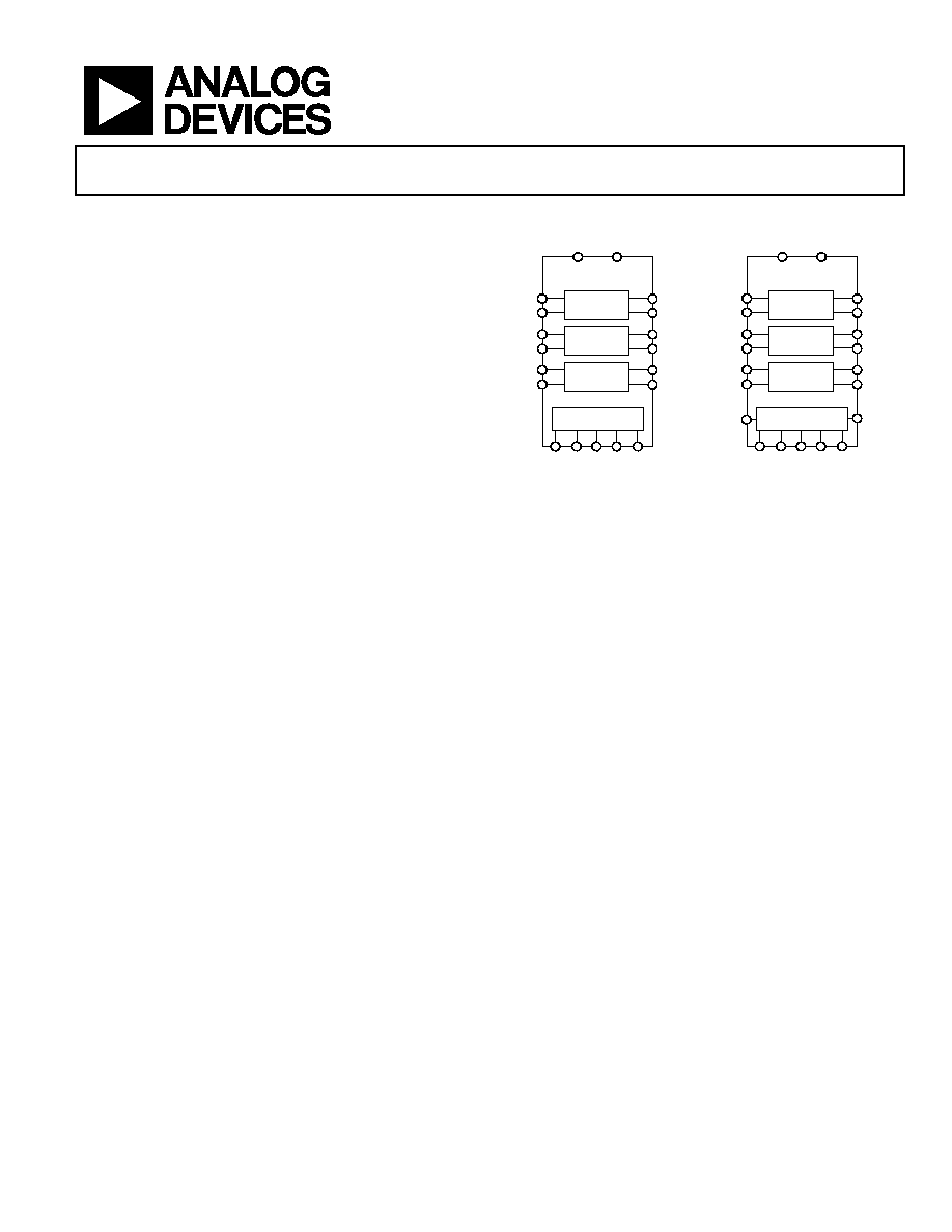
FUNCTIONAL BLOCK DIAGRAM
GPO2
SCL
SDA
A2
A1
A0
V
DD
GND
S3B
D3B
S3A
D3A
2 × 2
CROSSPOINT
S1B
D1B
S1A
D1A
2 × 2
CROSSPOINT
S2B
D2B
S2A
D2A
2 × 2
CROSSPOINT
ADG799G
06038-
001
GPO1
I
2
C SERIAL
INTERFACE
SCL
SDA
A2
A1
A0
V
DD
GND
I
2
C SERIAL
INTERFACE
S3B
D3B
S3A
D3A
2 × 2
CROSSPOINT
S1B
D1B
S1A
D1A
2 × 2
CROSSPOINT
S2B
D2B
S2A
D2A
2 × 2
CROSSPOINT
ADG799A
Figure 1.
GENERAL DESCRIPTION
The ADG799A/ADG799G are monolithic CMOS devices
comprising three 2x2 crosspoint switches controllable via a
standard I
2
C serial interface. The CMOS process provides
ultralow power dissipation, yet offers high switching speed and
low on resistance.
The on resistance profile is very flat over the full analog input
range and wide bandwidth ensures excellent linearity and low
distortion. These features, combined with a wide input signal
range, make the ADG799A/ADG799G the ideal switching
solution for a wide range of TV applications including RGB and
YPbPr video switches for picture-in picture applications.
The switches conduct equally well in both directions when on.
In the off condition, signal levels up to the supplies are blocked.
The ADG799A/ADG799G switches exhibit break-before-make
switching action. The ADG799G has two general-purpose logic
output pins controlled by the I
2
C interface that can also be used
to control other non I
2
C compatible devices such as video filters.
The integrated I
2
C interface provides a large degree of flexibility
in the system design. It has three user-adjustable I
2
C address
pins that allow up to eight devices on the same bus. This allows
the user to expand the capability of the device by increasing the
size of the switching array.
The ADG799A/ADG799G operate from single 3 V or 5 V
supply voltages and are available in a compact, 4 mm x 4 mm
body, 24-lead, lead-free LFCSP.
PRODUCT HIGHLIGHTS
1. Wide bandwidth: 230 MHz.
2. Ultralow power dissipation.
3. Extended input signal range.
4. Integrated
I
2
C serial interface.
5. Compact 4 mm x 4 mm, 24-lead, lead-free LFCSP.

ADG799A/ADG799G
Preliminary Technical Data
Rev. Pr.G | Page 2 of 23
TABLE OF CONTENTS
Features .............................................................................................. 1
Applications....................................................................................... 1
Functional Block Diagram .............................................................. 1
General Description ......................................................................... 1
Product Highlights ........................................................................... 1
Revision History ............................................................................... 2
Specifications..................................................................................... 3
I
2
C Timing Specifications............................................................ 7
Timing Diagram ........................................................................... 8
Absolute Maximum Ratings............................................................ 9
ESD Caution.................................................................................. 9
Pin Configurations and Function Descriptions ......................... 10
Typical Performance Characteristics ........................................... 11
Test Circuits..................................................................................... 14
Terminology .................................................................................... 16
Theory of Operation ...................................................................... 17
I
2
C Serial Interface ..................................................................... 17
I
2
C Address.................................................................................. 17
Write Operation.......................................................................... 17
LDSW Bit..................................................................................... 18
Power On/Software Reset.......................................................... 18
Read Operation........................................................................... 18
Evaluation Board ............................................................................ 20
Using the ADG799G Evaluation Board .................................. 20
Outline Dimensions ....................................................................... 23
Ordering Guide .......................................................................... 23
REVISION HISTORY
6/06--Revision 0: Initial Version
Preliminary Technical Data
ADG799A/ADG799G
Rev. Pr.G | Page 3 of 23
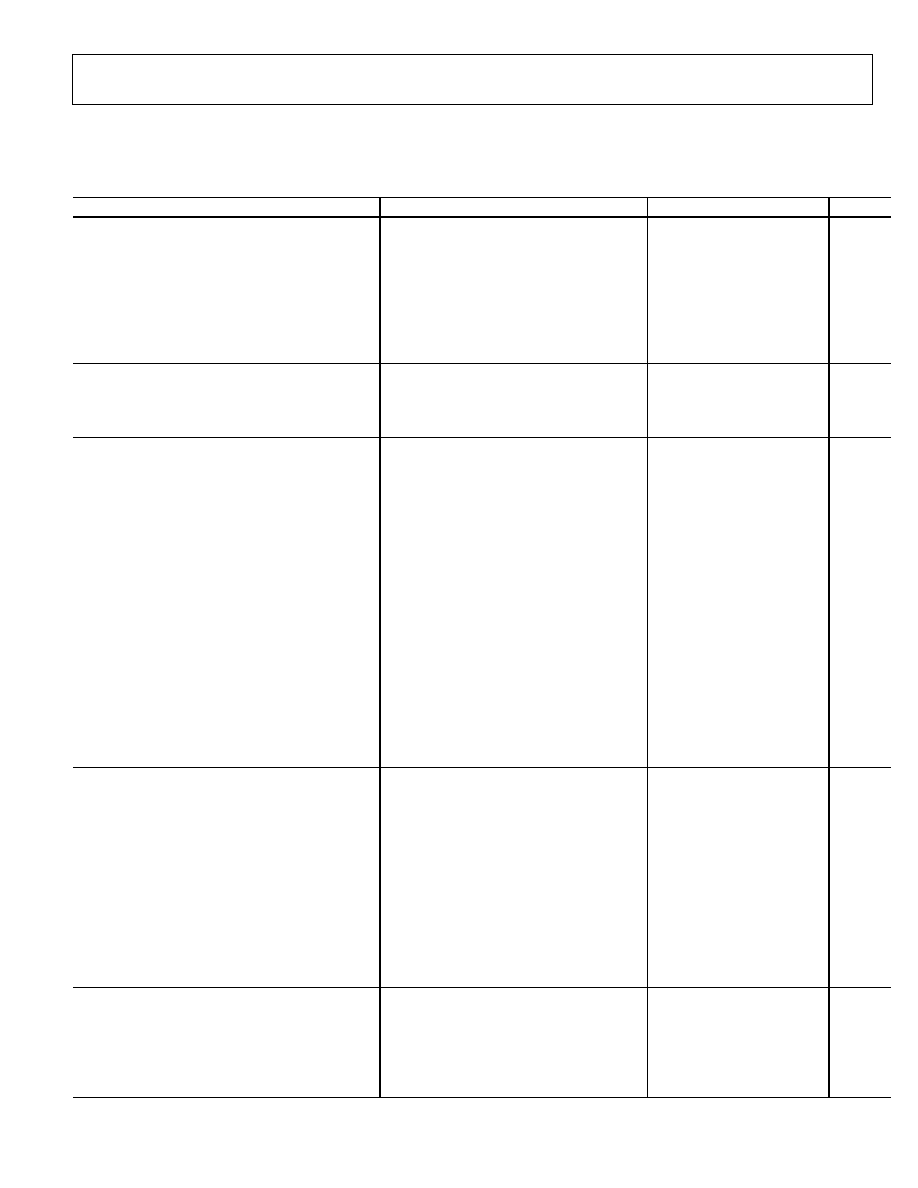
SPECIFICATIONS
V
DD
= 5 V ± 10%, GND = 0 V, T
A
= -40°C to +85°C, unless otherwise noted.
Table 1.
Parameter
Conditions
Min
Typ
1
Max
Units
ANALOG SWITCH
Analog Signal Range
2
V
S
= V
DD
, R
L
= 1 M
0
4
V
V
S
=V
DD
, R
L
= 75
0
3.3
V
On Resistance, R
ON
V
D
= 0 V, I
DS
= -10 mA, see Figure 22
2.6
5
V
D
= 0 V to 1 V, I
DS
= -10 mA, see Figure 22
5.5
On Resistance Matching Between Channels, R
ON
V
D
= 0 V, I
DS
= -10 mA
0.15
1.8
V
D
= 1 V, I
DS
= -10 mA
1.8
On Resistance Flatness, R
FLAT(ON)
V
D
= 0 V to 1 V, I
DS
= -10 mA
0.3
0.55
LEAKAGE CURRENTS
Source Off Leakage (I
S(OFF)
) V
D
= 4 V/1 V, V
S
= 1 V/4 V, see Figure 23
±0.25
nA
Drain Off Leakage (I
D(OFF)
) V
D
= 4 V/1 V, V
S
= 1 V/4 V, see Figure 23
±0.25
nA
Channel On Leakage (I
D(ON)
, I
S(ON)
) V
D
= V
S
= 4 V/1 V, see Figure 24
±0.25
nA
DYNAMIC CHARACTERISTICS
3
t
ON
, t
ENABLE
C
L
= 35 pF, R
L
= 50 , V
S
= 2 V, see Figure 25
184
240
ns
t
OFF
, t
DISABLE
C
L
= 35 pF, R
L
= 50 , V
S
= 2 V, see Figure 25
180
235
ns
Break-Before-Make Time Delay, t
D
C
L
= 35 pF, R
L
= 50 , V
S1
= V
S2
= 2 V, see Figure 26
1
3
ns
I
2
C to GPO Propagation Delay, t
H
, t
L
(ADG799G only)
130
ns
Off Isolation
f = 10 MHz, R
L
= 50 , see Figure 28
-60
dB
Channel-to-Channel Crosstalk
f = 10 MHz, R
L
= 50 , see Figure 29
Same Crosspoint Switch
-50
dB
Different Crosspoint Switch
-80
dB
-3 dB Bandwidth
R
L
= 50 , see Figure 27
230
MHz
THD + N
R
L
= 100
0.14
%
Charge Injection
C
L
= 1 nF, V
S
= 0 V, see Figure 30
4
pC
C
S(OFF)
13
pF
C
D(OFF)
17
pF
C
D(ON)
, C
S(ON)
35
pF
Power Supply Rejection Ratio, PSSR
f = 20 kHz
70
dB
Differential Gain Error
CCIR330 test signal
0.56
%
Differential Phase Error
CCIR330 test signal
0.79
°
LOGIC INPUTS
3
A0, A1, A2 Pins
Input High Voltage, V
INH
2.0
V
Input Low Voltage, V
INL
0.8
V
Input Current, I
INL
or I
INH
V
IN
= 0 V to V
DD
0.005
±1
µA
Input Capacitance, C
IN
3
pF
SCL, SDA Pins
Input High Voltage, V
INH
0.7 × V
DD
V
DD
+ 0.3
V
Input Low Voltage, V
INL
-0.3
0.3 × V
DD
V
Input Leakage Current, I
IN
V
IN
= 0 V to V
DD
0.005
±1
µA
Input Hysteresis
0.05 × V
DD
V
Input Capacitance, C
IN
3
pF
LOGIC OUTPUTS
SDA Pin
3
Output Low Voltage, V
OL
I
SINK
= 3 mA
0.4
V
I
SINK
= 6 mA
0.6
V
Floating State Leakage Current
±1
µA
Floating State Output Capacitance
10
pF

ADG799A/ADG799G
Preliminary Technical Data
Rev. Pr.G | Page 4 of 23
Parameter
Conditions
Min
Typ
1
Max
Units
GPO1 and GPO2 Pins
Output Low Voltage, V
OL
I
LOAD
= 2 mA
0.4
V
Output High Voltage, V
OH
I
LOAD
= -2 mA
2.0
V
POWER REQUIREMENTS
I
DD
Digital inputs = 0 V or V
DD
, I
2
C interface inactive
0.001
1
µA
I
2
C interface active, f
SCL
= 400 kHz
0.2
mA
I
2
C interface active, f
SCL
= 3.4 MHz
0.7
mA
1
All typical values are at T
A
= +25°C, unless otherwise stated.
2
Guaranteed by initial characterization, not subject to production test.
3
Guaranteed by design, not subject to production test.

Preliminary Technical Data
ADG799A/ADG799G
Rev. Pr.G | Page 5 of 23
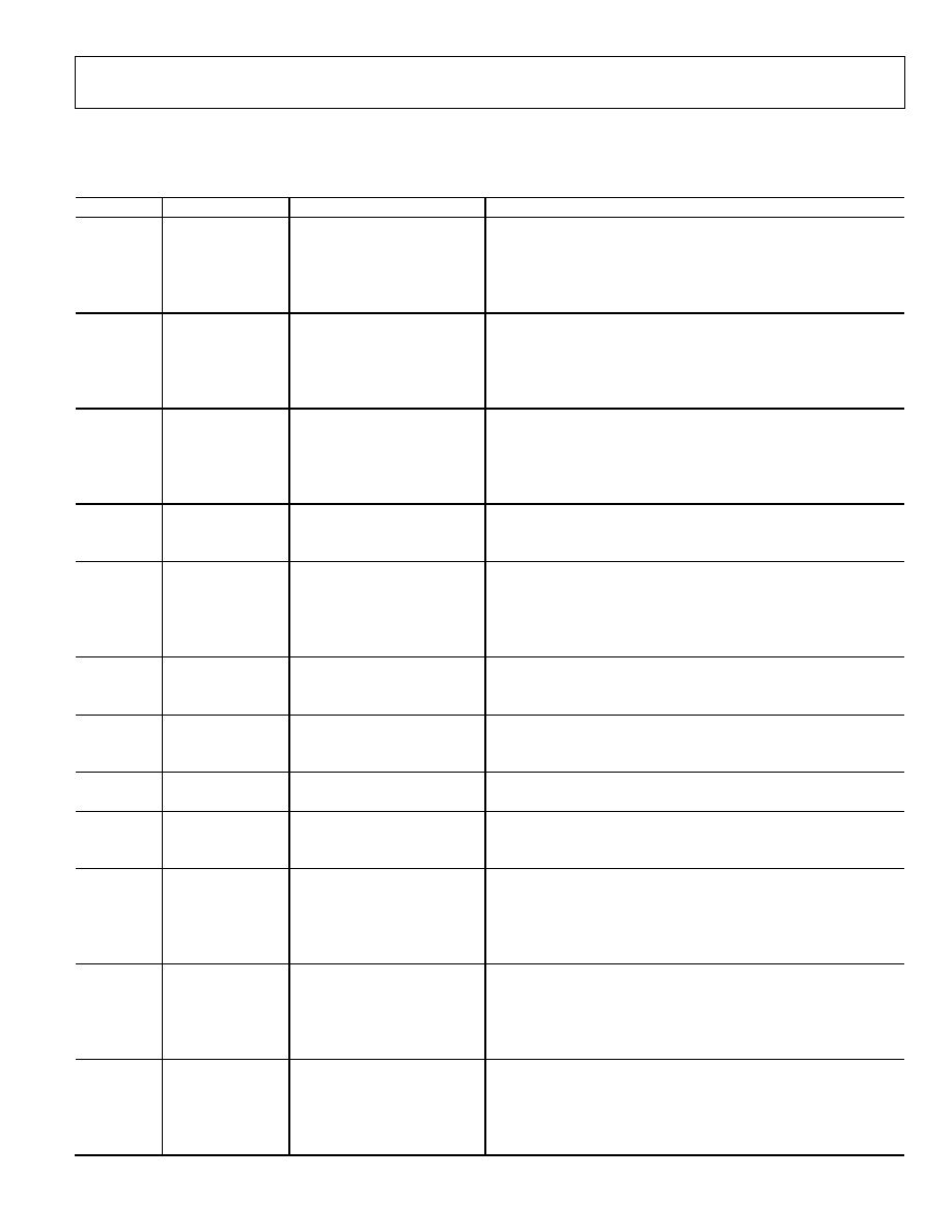
V
DD
= 3 V ± 10%, GND = 0 V, T
A
= -40°C to +85°C, unless otherwise noted.
Table 2.
Parameter
Conditions
Min
Typ
1
Max
Units
ANALOG SWITCH
Analog Signal Range
2
V
S
= V
DD
, R
L
= 1 M
0
2.4
V
V
S
= V
DD
, R
L
= 75
0
1.7
V
On Resistance, R
ON
V
D
= 0 V, I
DS
= -10 mA, see Figure 22
3
5.5
V
D
= 0 V to 1 V, I
DS
= -10 mA, see Figure 22
8
On Resistance Matching Between Channels, R
ON
V
D
= 0 V, I
DS
= -10 mA
0.15
1.8
V
D
= 1 V, I
DS
= -10 mA
2
On Resistance Flatness, R
FLAT(ON)
V
D
= 0 V to 1 V, I
DS
= -10 mA
0.3
2.8
LEAKAGE CURRENTS
Source Off Leakage (I
S(OFF)
) V
D
= 2 V/1 V, V
S
= 1 V/2 V, see Figure 23
±0.25
nA
Drain Off Leakage (I
D(OFF)
) V
D
= 2 V/1 V, V
S
= 1 V/2 V, see Figure 23
±0.25
nA
Channel On Leakage (I
D(ON)
, I
S(ON)
) V
D
= V
S
= 2 V/1 V, see Figure 24
±0.25
nA
DYNAMIC CHARACTERISTICS
3
t
ON
, t
ENABLE
C
L
= 35 pF, R
L
= 50 , V
S
= 2 V, see Figure 25
203
266
ns
t
OFF
, t
DISABLE
C
L
= 35 pF, R
L
= 50 , V
S
= 2 V, see Figure 25
200
260
ns
Break-Before-Make Time Delay, t
D
C
L
= 35 pF, R
L
= 50 , V
S1
= V
S2
= 2 V, see Figure 26
1
3
ns
I
2
C to GPO Propagation Delay, t
H
, t
L
(ADG799G only)
121
ns
Off Isolation
f = 10 MHz, R
L
= 50 , see Figure 28
-60
dB
Channel-to-Channel Crosstalk
f = 10 MHz, R
L
= 50 , see Figure 29
Same Crosspoint Switch
-50
dB
Different Crosspoint Switch
-80
dB
-3 dB Bandwidth
R
L
= 50 , see Figure 27
210
MHz
THD + N
R
L
= 100
0.14
%
Charge Injection
C
L
= 1 nF, V
S
= 0 V, see Figure 30
2
pC
C
S(OFF)
13
pF
C
D(OFF)
17
pF
C
D(ON)
, C
S(ON)
35
pF
Power Supply Rejection Ratio, PSSR
f = 20 kHz
70
dB
Differential Gain Error
CCIR330 test signal
0.66
%
Differential Phase Error
CCIR330 test signal
1
°
LOGIC INPUTS
A0, A1, A2 Pins
3
Input High Voltage, V
INH
2.0
V
Input Low Voltage, V
INL
0.8
V
Input Current, I
INL
or I
INH
V
IN
= 0 V to V
DD
0.005
±1
µA
Input Capacitance, C
IN
3
pF
SCL, SDA Pins
3
Input High Voltage, V
INH
0.7 × V
DD
V
DD
+ 0.3
V
Input Low Voltage, V
INL
-0.3
0.3 × V
DD
V
Input Leakage Current, I
IN
V
IN
= 0 V to V
DD
0.005
±1
µA
Input Hysteresis
0.05 × V
DD
V
Input Capacitance, C
IN
3
pF
LOGIC OUTPUTS
3
SDA Pin
Output Low Voltage, V
OL
I
SINK
= 3 mA
0.4
V
I
SINK
= 6 mA
0.6
V
Floating State Leakage Current
±1
µA
Floating State Output Capacitance
3
pF

ADG799A/ADG799G
Preliminary Technical Data
Rev. Pr.G | Page 6 of 23
Parameter
Conditions
Min
Typ
1
Max
Units
GPO1 and GPO2 Pins
Output Low Voltage, V
OL
I
LOAD
= 2 mA
0.4
V
Output High Voltage, V
OH
I
LOAD
= -2 mA
2.0
V
POWER REQUIREMENTS
I
DD
Digital inputs = 0 V or V
DD
, I
2
C interface inactive
0.001
1
µA
I
2
C interface active, f
SCL
= 400 kHz
0.1
mA
I
2
C interface active, f
SCL
= 3.4 MHz
0.2
mA
1
All typical values are at T
A
= +25°C, unless otherwise stated.
2
Guaranteed by initial characterization, not subject to production test.
3
Guaranteed by design, not subject to production test.
Preliminary Technical Data
ADG799A/ADG799G
Rev. Pr.G | Page 7 of 23
I
2
C TIMING SPECIFICATIONS
V
DD
= 2.7 V to 5.5 V; GND = 0 V; T
A
= -40°C to +85°C, unless otherwise noted (see Figure 2 for timing diagram).
Table 3.
Parameter
1
Conditions
Min
Max
Unit
Description
f
SCL
Standard mode
100
kHz
Serial clock frequency
Fast mode
400
kHz
High speed mode
C
B
= 100 pF max
3.4
MHz
C
B
= 400 pF max
1.7
MHz
t
1
Standard mode
4
µs
t
HIGH
, SCL high time
Fast mode
0.6
µs
High speed mode
C
B
= 100 pF max
60
ns
C
B
= 400 pF max
120
ns
t
2
Standard mode
4.7
µs
t
LOW
, SCL low time
Fast mode
1.3
µs
High speed mode
C
B
= 100 pF max 160
ns
C
B
= 400 pF max 320
ns
t
3
Standard mode
250
ns
t
SU;DAT
, data setup time
Fast mode
100
ns
High speed mode
10
ns
t
4
2
Standard mode
0
3.45
µs
t
HD;DAT
, data hold time
Fast mode
0
0.9
µs
High speed mode
C
B
= 100 pF max
0
703
ns
C
B
= 400 pF max 0
150
ns
t
5
Standard mode
4.7
µs
t
SU;STA
, setup time for a repeated start condition
Fast mode
0.6
µs
High speed mode
160
ns
t
6
Standard mode
4
µs
t
HD;STA
, hold time (repeated) start condition
Fast mode
0.6
µs
High speed mode
160
ns
t
7
Standard mode
4.7
µs
t
BUF
, bus free time between a stop and a start condition
Fast mode
1.3
µs
t
8
Standard mode
4
µs
t
SU;STO
, setup time for stop condition
Fast mode
0.6
µs
High speed mode
160
ns
t
9
Standard mode
1000
ns
t
RDA
, rise time of SDA signal
Fast mode
20 + 0.1 C
B
300
ns
High speed mode
C
B
= 100 pF max 10
80
ns
C
B
= 400 pF max 20
160
ns
t
10
Standard mode
300
ns
t
FDA
, fall time of SDA signal
Fast mode
20 + 0.1 C
B
300 ns
High speed mode
C
B
= 100 pF max
10
80
ns
C
B
= 400 pF max
20
160
ns
t
11
Standard mode
1000
ns
t
RCL
, rise time of SCL signal
Fast mode
20 + 0.1 C
B
300 ns
High speed mode
C
B
= 100 pF max
10
40
ns
C
B
= 400 pF max
20
80
ns
ADG799A/ADG799G
Preliminary Technical Data
Rev. Pr.G | Page 8 of 23
Parameter
1
Conditions
Min
Max
Unit
Description
t
11A
Standard mode
1000
ns
t
RCL1
, rise time of SCL signal after a repeated start condition and after
Fast mode
20 + 0.1 C
B
300
ns
an acknowledge bit.
High speed mode
C
B
= 100 pF max
10
80
ns
C
B
= 400 pF max
20
160
ns
t
12
Standard mode
300
ns
t
FCL
, fall time of SCL signal
Fast mode
20 + 0.1 C
B
300 ns
High speed mode
C
B
= 100 pF max
10
40
ns
C
B
= 400 pF max
20
80
ns
t
SP
Fast mode
0
50
ns
Pulse width of suppressed spike
High speed mode
0
10
ns
1
Guaranteed by initial characterization. CB refers to capacitive load on the bus line, tr and tf measured between 0.3 V
DD
and 0.7 V
DD
.
2
A device must provide a data hold time for SDA in order to bridge the undefined region of the SCL falling edge.
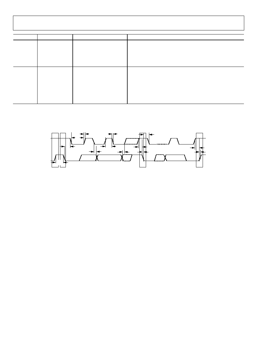
TIMING DIAGRAM
SCL
SDA
P
S
S
P
t
8
t
6
t
5
t
3
t
10
t
9
t
4
t
6
t
1
t
7
t
2
t
11
t
12
0
60
38
-
0
02
Figure 2. Timing Diagram for 2-Wire Serial Interface
Preliminary Technical Data
ADG799A/ADG799G
Rev. Pr.G | Page 9 of 23
ABSOLUTE MAXIMUM RATINGS
T
A
= 25°C, unless otherwise noted.
Table 4.
Parameter Rating
V
DD
to GND
-0.3 V to +6 V
Analog, Digital Inputs
-0.3 V to V
DD
+ 0.3 V or 30 mA,
whichever occurs first
Continuous Current, S or D Pins
100 mA
Peak Current, S or D Pins
300 mA (pulsed at 1 ms,
10% duty cycle max)
Operating Temperature Range
Industrial (B Version)
-40°C to +85°C
Storage Temperature Range
-65°C to +150°C
Junction Temperature
150°C
JA
Thermal Impedance
24-Lead LFCSP
30°C/W
Lead Temperature, Soldering
(10 sec)
300°C
IR Reflow, Peak Temperature
(<20 sec)
260°C
Stresses above those listed under Absolute Maximum Ratings
may cause permanent damage to the device. This is a stress
rating only; functional operation of the device at these or any
other conditions above those indicated in the operational
section of this specification is not implied. Exposure to absolute
maximum rating conditions for extended periods may affect
device reliability.
Only one absolute maximum rating can be applied at any one
time.
ESD CAUTION
ESD (electrostatic discharge) sensitive device. Electrostatic charges as high as 4000 V readily accumulate on
the human body and test equipment and can discharge without detection. Although this product features
proprietary ESD protection circuitry, permanent damage may occur on devices subjected to high energy
electrostatic discharges. Therefore, proper ESD precautions are recommended to avoid performance
degradation or loss of functionality.
ADG799A/ADG799G
Preliminary Technical Data
Rev. Pr.G | Page 10 of 23
PIN CONFIGURATIONS AND FUNCTION DESCRIPTIONS
PIN 1
INDICATOR
1
NC
2
S1A
3
D1A
4
D1B
5
S1B
6
NC
15 D3A
16 D3B
17 S3B
18 A2
14 S3A
13 NC
7
N
C
8
S
2
A
9
D
2
A
1
1
S
2
B
1
2
N
C
1
0
D
2
B
2
1
S
C
L
2
2
S
D
A
2
3
V
D
D
2
4
G
N
D
2
0
A
0
1
9
A
1
ADG799A
TOP VIEW
(Not to Scale)
NOTES
1. NC = NO CONNECT.
2. THE EXPOSED PAD MUST BE TIED TO GND.
06
03
8-
0
3
4
Figure 3. ADG799A Pin Configuration
PIN 1
INDICATOR
NOTES
1. NC = NO CONNECT.
2. THE EXPOSED PAD MUST BE TIED TO GND.
1
NC
2
S1A
3
D1A
4
D1B
5
S1B
6
GPO2
15 D3A
16 D3B
17 S3A
18 A2
14 S3B
13 NC
7
N
C
8
S
2
A
9
D
2
A
1
1
S
2
B
1
2
G
P
O
1
1
0
D
2
B
2
1
S
C
L
2
2
S
D
A
2
3
V
D
D
2
4
G
N
D
2
0
A
0
1
9
A
1
ADG799G
TOP VIEW
(Not to Scale)
06
03
8-
01
2
Figure 4. ADG799G Pin Configuration
Table 5. Pin Function Descriptions
Pin No.
Mnemonic
Function
1
NC
Not internally connected.
2
S1A
A-Side Source Terminal for Crosspoint Switch 1. Can be an input or output.
3
D1A
A-Side Drain Terminal for Crosspoint Switch 1. Can be an input or output.
4
D1B
B-Side Drain Terminal for Crosspoint Switch 1. Can be an input or output.
5
S1B
B-Side Source Terminal for Crosspoint Switch 1. Can be an input or output.
6
NC/GPO2
Not internally connected (for the ADG799A) / General-Purpose Logic Output 2 (for the ADG799G).
7
NC
Not internally connected.
8
S2A
A-Side Source Terminal for Crosspoint Switch 2. Can be an input or output.
9
D2A
A-Side Drain Terminal for Crosspoint Switch 2. Can be an input or output.
10
D2B
B-Side Drain Terminal for Crosspoint Switch 2. Can be an input or output.
11
S2B
B-Side Source Terminal for Crosspoint Switch 2. Can be an input or output.
12
NC/GPO1
Not internally connected (for the ADG799A) / General-Purpose Logic Output 1 (for the ADG799G).
13
NC
Not internally connected.
14
S3B
B-Side Source Terminal for Crosspoint Switch 3. Can be an input or output.
15
D3A
A-Side Drain Terminal for Crosspoint Switch 3. Can be an input or output
16
D3B
B-Side Drain Terminal for Crosspoint Switch 3. Can be an input or output.
17
S3A
A-Side Source Terminal for Crosspoint Switch 3. Can be an input or output.
18
A2
Logic Input. Sets Bit A2 from the least significant bits of the 7-bit slave address.
19
A1
Logic Input. Sets Bit A1 from the least significant bits of the 7-bit slave address.
20
A0
Logic Input. Sets Bit A0 from the least significant bits of the 7-bit slave address.
21 SCL
Digital Input, Serial Clock Line. Open drain input that is used in conjunction with SDA to clock data into the device.
External pull-up resistor required.
22
SDA
Digital Input/Output. Bidirectional open drain data line. External pull-up resistor required.
23 V
DD
Positive Power Supply Input.
24
GND
Ground (0 V) Reference.
Preliminary Technical Data
ADG799A/ADG799G
Rev. Pr.G | Page 11 of 23
TYPICAL PERFORMANCE CHARACTERISTICS
0
60
38
-
0
1
8
3.0
0
0
3.5
INPUT SIGNAL (V)
OU
TP
U
T
S
I
GN
A
L
(
V
)
2.5
2.0
1.5
1.0
0.5
0.5
1.0
1.5
2.0
2.5
3.0
T
A
= 25°C
1 CHANNEL
V
DD
= 3.3V, R
L
= 1M
V
DD
= 3.0V, R
L
= 1M
V
DD
= 2.7V, R
L
= 1M
V
DD
= 3.3V, R
L
= 75
V
DD
= 3.0V, R
L
= 75
V
DD
= 2.7V, R
L
= 75
Figure 5. Analog Signal Range, 3 V Supply
0
60
38
-
0
1
9
5.0
0
0
6
INPUT SIGNAL (V)
O
U
T
P
UT
S
I
G
NAL
(
V
)
4.5
4.0
3.5
3.0
2.5
2.0
1.5
1.0
0.5
1
2
3
4
5
T
A
= 25°C
1 CHANNEL
V
DD
= 5.5V, R
L
= 1M
V
DD
= 5.0V, R
L
= 1M
V
DD
= 4.5V, R
L
= 1M
V
DD
= 5.5V, R
L
= 75
V
DD
= 5.0V, R
L
= 75
V
DD
= 4.5V, R
L
= 75
Figure 6. Analog Signal Range, 5 V Supply
06
03
8
-
02
0
6
0
0
1.8
V
D
(V
S
) (V)
R
ON
(
)
5
4
3
2
1
0.2
0.4
0.6
0.8
1.0
1.2
1.4
1.6
T
A
= 25°C
1 CHANNEL
V
DD
= 2.7V
V
DD
= 3.3V
V
DD
= 3.0V
Figure 7. On Resistance vs. V
D
(V
S
), 3 V Supply
06
03
8
-
02
1
4.0
0
0
3.0
V
D
(V
S
) (V)
R
ON
(
)
3.5
3.0
2.5
2.0
1.5
1.0
0.5
0.5
1.0
1.5
2.0
2.5
T
A
= 25°C
1 CHANNEL
V
DD
= 4.5V
V
DD
= 5.5V
V
DD
= 5.0V
Figure 8. On Resistance vs. V
D
(V
S
), 5 V Supply
06
03
8-
0
2
2
7
0
0
1.6
V
D
(V
S
) (V)
R
ON
(
)
6
5
4
3
2
1
0.2
0.4
0.6
0.8
1.0
1.2
1.4
T
A
= 25°C
1 CHANNEL
V
DD
= 3V
T
A
= +25°C
T
A
= +85°C
T
A
= 40°C
Figure 9. On Resistance vs. V
D
(V
S
) for Various Temperatures, 3 V Supply
06
038
-
0
2
3
4.5
0
0
3.0
V
D
(V
S
) (V)
R
ON
(
)
4.0
3.5
3.0
2.5
2.0
1.5
1.0
0.5
0.5
1.0
1.5
2.0
2.5
T
A
= +25°C
1 CHANNEL
V
DD
= 5V
T
A
= +25°C
T
A
= +85°C
T
A
= 40°C
Figure 10. On Resistance vs. V
D
(V
S
) for Various Temperatures, 5 V Supply
ADG799A/ADG799G
Preliminary Technical Data
Rev. Pr.G | Page 12 of 23
0
60
38
-
0
2
9
0
4.0
0
3.5
SOURCE VOLTAGE (V)
C
HARG
E
I
N
JE
C
T
I
O
N (
p
C)
0.5
1.0
1.5
2.0
2.5
3.0
T
A
= 25°C
0.5
1.0
1.5
2.0
2.5
3.0
3.5
V
DD
= 3V
V
DD
= 5V
Figure 11. Charge Injection vs. Source Voltage
0
60
38
-
0
3
0
225
215
205
195
185
175
165
TEMPERATURE (°C)
t
ON
/
t
OF
F
(n
s
)
40
20
0
20
40
60
80
t
ON
(3V)
t
ON
(5V)
t
OFF
(3V)
t
OFF
(5V)
Figure 12. T
ON
/T
OFF
vs. Temperature
0
60
38
-
0
3
1
0
120
0.01
1000
FREQUENCY (MHz)
OF
F-
I
S
OL
A
T
IO
N
(
d
B
)
20
40
60
80
100
0.1
1
10
100
T
A
= 25°C
V
DD
= 3V/5V
Figure 13. Off Isolation vs. Frequency
0
60
38
-
0
3
2
0
120
0.01
1000
FREQUENCY (MHz)
CR
O
S
S
T
A
L
K (
d
B
)
20
40
60
80
100
0.1
1
10
100
SAME
CROSS POINT
SWITCH
DIFFERENT
CROSS POINT
SWITCH
T
A
= 25°C
V
DD
= 3V/5V
Figure 14. Crosstalk vs. Frequency
0
60
38
-
0
3
3
0
20
0.1
1000
FREQUENCY (MHz)
A
T
T
E
NUA
T
I
O
N
(
d
B)
1
10
100
18
16
14
12
10
8
6
4
2
T
A
= 25°C
V
DD
= 5V
Figure 15. Bandwidth
06
03
8-
0
2
4
0
100
0.0001
1000
FREQUENCY (MHz)
PS
SR
(d
B
)
10
20
30
40
50
60
70
80
90
0.001
0.01
0.1
1
10
100
T
A
= 25°C
1 CHANNEL
V
DD
= 3V/5V
NO DECOUPLING CAPACITORS USED
Figure 16. PSSR vs. Frequency

Preliminary Technical Data
ADG799A/ADG799G
Rev. Pr.G | Page 13 of 23
0
603
8-
0
2
5
0.40
0
0.1
3.1
f
CLK
FREQUENCY (MHz)
I
DD
(m
A
)
0.35
0.30
0.25
0.20
0.15
0.10
0.05
0.6
1.1
1.6
2.1
2.6
V
DD
= 3V
V
DD
= 5V
T
A
= 25°C
Figure 17. I
DD
vs. f
CLK
frequency
0
60
38
-
0
2
6
1.4
0.2
0
6
I
2
C LOGIC INPUT VOLTAGE (V)
I
DD
(m
A
)
1.2
1.0
0.8
0.6
0.4
0.2
0
1
2
3
4
5
T
A
= 25°C
V
DD
= 3V
V
DD
= 5V
Figure 18. I
DD
vs. I
2
C Logic Input Voltage (SDA, SCL)
120
95
40
20
0
20
40
60
80
TEMPERATURE (°C)
P
R
O
P
AG
AT
I
O
N DE
L
A
Y
(
n
s)
115
110
105
100
t
PLH
(5V)
t
PHL
(3V)
t
PLH
(3V)
t
PHL
(5V)
0
603
3-
0
1
9
Figure 19. I
2
C to GPO Propagation Delay vs. Temperature
(ADG799G Only)
0
60
38
-
0
2
7
6
0
20
0
LOAD CURRENT (mA)
GP
O
V
O
LT
A
G
E
(
V
)
5
4
3
2
1
18
16
14
12
10
8
6
4
2
T
A
= 25°C
V
DD
= 3V
V
DD
= 5V
Figure 20. GPO V
OH
vs. Load Current
0
60
38
-
0
2
8
2.5
0
0
35
LOAD CURRENT (mA)
GP
O
V
O
LT
A
G
E
(
V
)
2.0
1.5
1.0
0.5
5
10
15
20
25
30
T
A
= 25°C
V
DD
= 3V
V
DD
= 5V
Figure 21. GPO V
OL
vs. Load Current
ADG799A/ADG799G
Preliminary Technical Data
Rev. Pr.G | Page 14 of 23
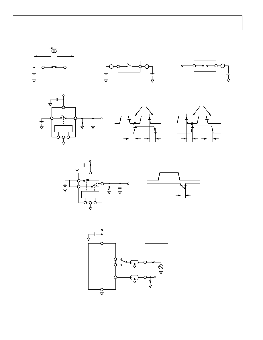
TEST CIRCUITS
S
D
R
ON
= V1/I
DS
V1
I
DS
V
S
06
03
8-
0
0
3
S
D
A
A
I
S
(OFF)
V
S
V
D
I
D
(OFF)
060
38
-
0
0
4
S
D
A
V
D
I
D
(ON)
NC
NC = NO CONNECT
06
03
8-
0
0
5
Figure 22. On Resistance
Figure 23. Off Leakage
Figure 24. On Leakage
06
03
8-
00
6
I
2
C
INTERFACE
SCL
GND
SDA
V
S
C
L
35pF
R
L
50
V
OUT
V
DD
5V
0.1µF
S
D
SCL
50%
50%
90%
10%
t
OFF
t
ON
V
OUT
CLOCK PULSES
CORRESPONDING
TO THE LDSW BITS
50%
50%
90%
10%
t
H
t
L
SCL
V
GPO
CLOCK PULSES
CORRESPONDING
TO THE LDSW BITS
Figure 25. Switching Times
I
2
C
INTERFACE
SCL
GND
SDA
C
L
35pF
R
L
100
V
S
V
OUT
V
DD
5V
0.1µF
SA
D
SB
SCL
CLOCK PULSES CORRESPONDING
TO THE LDSW BIT
V
S
t
D
V
OUT
80%
06
03
8-
00
7
Figure 26. Break-Before-Make Time Delay
V
DD
0.1µF
V
S
50
50
50
D
V
OUT
50
NETWORK
ANALYZER
GND
SA
SB
06
03
8-
00
8
Figure 27. Bandwidth
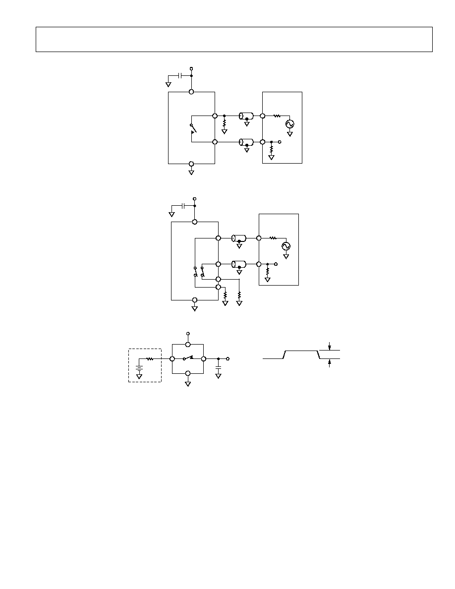
Preliminary Technical Data
ADG799A/ADG799G
Rev. Pr.G | Page 15 of 23
S
D
V
DD
0.1µF
V
S
V
OUT
50
50
50
50
50
NETWORK
ANALYZER
GND
06
03
8-
00
9
Figure 28. Off Isolation
SY
DY
DX
SX
V
DD
0.1µF
V
S
V
OUT
50
50
50
R
L
50
NETWORK
ANALYZER
GND
50
50
06
03
8-
0
1
0
Figure 29. Channel-to-Channel Crosstalk
V
S
V
OUT
GND
V
DD
R
S
5V
S
D
C
L
1nF
V
OUT
Q
INJ
= C
L
× V
OUT
SWITCH ON
SWITCH OFF
06
03
8-
0
1
1
Figure 30. Charge Injection

ADG799A/ADG799G
Preliminary Technical Data
Rev. Pr.G | Page 16 of 23
TERMINOLOGY
On Resistance (R
ON
)
The series on-channel resistance measured between the S and
D pins.
On Resistance Match (R
ON
)
The channel-to-channel matching of on resistance when
channels are operated under identical conditions.
On Resistance Flatness (R
FLAT(ON)
)
The variation of on resistance over the specified range produced
by the specified analog input voltage change with a constant
load current.
Channel Off Leakage (I
OFF
)
The sum of leakage currents into or out of an off channel input.
Channel On Leakage (I
ON
)
The current loss/gain through an on-channel resistance,
creating a voltage offset across the device.
Input Leakage Current (I
IN
, I
INL
, I
INH
)
The current flowing into a digital input when a specified low
level or high level voltage is applied to that input.
Input/Output Off Capacitance (C
OFF
)
The capacitance between an analog input and ground when the
switch channel is off.
Input/Output On Capacitance (C
ON
)
The capacitance between the inputs or outputs and ground
when the switch channel is on.
Digital Input Capacitance (C
IN
)
The capacitance between a digital input and ground.
Output On Switching Time (t
ON
)
The time required for the switch channel to close. The time is
measured from 50% of the falling edge of the LDSW bit to the
time the output reaches 90% of the final value.
Output Off Switching Time (t
OFF
)
The time required for the switch to open. The time is measured
from 50% of the falling edge of the LDSW bit to the time the
output reaches 10% of the final value.
I
2
C to GPO propagation delay (t
H
, t
L
)
The time required for the logic value at the GPO pin to settle
after loading a GPO command. The time is measured from 50%
of the falling edge of the LDSW bit to the time the output
reaches 90% of the final value for high and 10% for low.
Total Harmonic Distortion + Noise (THD + N)
The ratio of the harmonic amplitudes plus noise of a signal to
the fundamental.
-3 dB Bandwidth
The frequency at which the output is attenuated by 3 dB.
Off Isolation
The measure of unwanted signal coupling through an off switch.
Crosstalk
The measure of unwanted signal that is coupled through from
one channel to another as a result of parasitic capacitance.
Charge Injection
The measure of the glitch impulse transferred from the digital
input to the analog output during on/off switching.
Differential Gain Error
The measure of how much color saturation shift occurs when
the luminance level changes. Both attenuation and amplifica-
tion can occur; therefore, the largest amplitude change between
any two levels is specified and expressed in %.
Differential Phase Error
The measure of how much hue shift occurs when the luminance
level changes. It can be a negative or positive value and is expressed
in degrees of subcarrier phase.
Input High Voltage (V
INH
)
The minimum input voltage for Logic 1.
Input Low Voltage (V
INL
)
The maximum input voltage for Logic 0.
Output High Voltage (V
OH
)
The minimum output voltage for Logic 1.
Output Low Voltage (V
OL
)
The maximum output voltage for Logic 0.
I
DD
Positive supply current.
Preliminary Technical Data
ADG799A/ADG799G
Rev. Pr.G | Page 17 of 23
THEORY OF OPERATION
The ADG799A/ADG799G are monolithic CMOS device
comprising three 2x2 crosspoint switches controllable via a
standard I
2
C serial interface. The CMOS process provides
ultralow power dissipation, yet offers high switching speed and
low on resistance.
The on resistance profile is very flat over the full analog input
range, and wide bandwidth ensures excellent linearity and low
distortion. These features, combined with a wide input signal
range, make the ADG799A/ADG799G an ideal switching
solution for a wide range of TV applications.
The switches conduct equally well in both directions when on.
In the off condition, signal levels up to the supplies are blocked.
The integrated serial I
2
C interface controls the operation of the
crosspoint switches (ADG799A/ADG799G) and general-
purpose logic pins (ADG799G only).
The ADG799A/ADG799G have many attractive features, such
as the ability to individually control each multiplexer, the option
of reading back the status of any switch. The ADG799G has two
general-purpose logic output pins controllable through the I
2
C
interface. The following sections describe these features in more
detail.
I
2
C SERIAL INTERFACE
The ADG799A/ADG799G are controlled via an I
2
C-compatible
serial bus interface (refer to the I
2
C-Bus Specification available
from Philips Semiconductor) that allows the part to operate as a
slave device (no clock is generated by the ADG799A/ADG799G).
The communication protocol between the I
2
C master and the
device operates as follows:
1. The master initiates data transfer by establishing a start
condition (defined as a high-to-low transition on the SDA
line while SCL is high). This indicates that an address/data
stream follows. All slave devices connected to the bus
respond to the start condition and shift in the next eight
bits, consisting of a seven bit address (MSB first) plus an
R/W bit. This bit determines the direction of the data flow
during the communication between the master and the
addressed slave device.
2. The slave device whose address corresponds to the
transmitted address responds by pulling the SDA line
low during the ninth clock pulse (this is known as the
acknowledge bit).
3. At this stage, all other devices on the bus remain idle while
the selected device waits for data to be written to, or read
from, its serial register. If the R/W bit is set high, the
master reads from the slave device. However, if the R/W bit
is set low, the master writes to the slave device.
4. Data transmits over the serial bus in sequences of nine
clock pulses (eight data bits followed by an acknowledge
bit). The transitions on the SDA line must occur during the
low period of the clock signal, SCL, and remain stable
during the high period of SCL. Otherwise, a low-to-high
transition when the clock signal is high can be interpreted
as a stop event that ends the communication between the
master and the addressed slave device.
5. After transferring all data bytes, the master establishes a
stop condition, defined as a low-to-high transition on the
SDA line while SCL is high. In write mode, the master pulls
the SDA line high during the 10
th
clock pulse to establish a
stop condition. In read mode, the master issues a no
acknowledge for the ninth clock pulse (the SDA line
remains high). The master then brings the SDA line low
before the 10
th
clock pulse, and then high during the 10
th
clock pulse to establish a stop condition.
I
2
C ADDRESS
The ADG799A/ADG799G each have a seven-bit I
2
C address.
The four most significant bits are internally hardwired while the
last three bits (A0, A1, and A2) are user-adjustable. This allows
the user to connect up to eight ADG799A/ADG799Gs to the
same bus. Table 6 shows the configuration of the seven-bit
address.
Table 6. Seven-Bit I
2
C Address Bit Configuration
MSB
LSB
1 0 1 0 A2
A1
A0
WRITE OPERATION
When writing to the ADG799A/ADG799G, the user must
begin with an address byte and R/W bit. Next, the switch
acknowledges that it is prepared to receive data by pulling SDA
low. Data is loaded into the device as a 16-bit word under the
control of a serial clock input, SCL. Figure 31 illustrates the
entire write sequence for the ADG799A/ADG799G. The first
data byte (AX7 to AX0) controls the status of the crosspoint
switches and the GPO pins, while the LDSW and RESTB bits
from the second byte controls the operation mode of the device.
Table 7 shows a list of all commands supported by the
ADG799A/ADG799G with the corresponding byte that needs
to be loaded during a write operation.
To achieve the desired configuration, one or more commands
can be loaded into the device. Any combination of the
commands listed in Table 7 can be used with the following
restrictions:
ADG799A/ADG799G
Preliminary Technical Data
Rev. Pr.G | Page 18 of 23
· The commands referring to more than one switch will
overwrite any previous command.
· When a sequence of successive commands affect the same
element (that is, the switch or GPO pin), only the last
command is executed.
LDSW BIT
The LDSW bit allows the user to control the way the device
executes the commands loaded during the write operations.
The ADG799A/ADG799G executes all the commands loaded
between two successive write operations that have set the
LDSW bit high.
Setting the LDSW high for every write cycle ensures that the
device executes the command right after the LDSW bit was
loaded into the device. This setting can be used when the
desired configuration can be achieved by sending a single
command or when the switches and/or GPO pins are not
required to be updated at the same time. When the desired
configuration requires multiple commands with simultaneous
update, the LDSW bit should be set low while loading the
commands except the last one when the LDSW bit should be set
high. Once the last command with LDSW=High is loaded, the
device will execute all commands received since the last update
simultaneously.
POWER ON/SOFTWARE RESET
The ADG799A/ADG799G has a software reset function
implemented by the RESETB bit from the second data byte
written to the device. For normal operation of the crosspoint
switch and GPO pins, this bit should be set high. When RESETB =
low or after power-up, the switches from all crosspoint switch
pins are turned off (open) and the GPO pins are set low.
READ OPERATION
When reading data back from the ADG799A/ADG799G, the
user must begin with an address byte and R/W bit. The switch
then acknowledges that it is prepared to transmit data by
pulling SDA low. Following this acknowledgement, the
ADG799A/ADG799G transmits two bytes on the next clock
edges. These bytes contain the status of the switches, and each
byte is followed by an acknowledge bit. A logic high bit
represents a switch in the on (close) state while a low represents
a switch in the off (open) state. For the GPO pins (ADG799G
only), the bit represents the logic value of the pin. Figure 32
illustrates the entire read sequence.
The bit maps accompanying Figure 32 show the relationship
between the elements of the ADG799A and ADG799G (that it,
the switches and GPO pins) and the bits that represent their
status after a completed read operation.
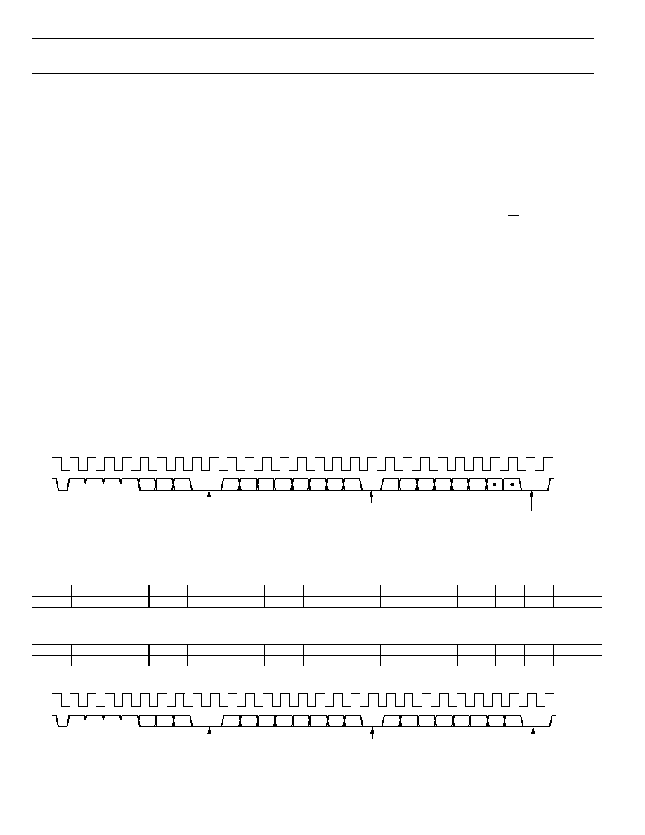
SCL
SDA
A2
A1
A0
AX6
AX7
R/W
AX5 AX4 AX3 AX2 AX1 AX0
X
X
X
X
X
X
RESETB
LDSW
START
CONDITION
BY MASTER
STOP
CONDITION
BY MASTER
ADDRESS BYTE
ACKNOWLEDGE
BY SWITCH
ACKNOWLEDGE
BY SWITCH
ACKNOWLEDGE
BY SWITCH
06
03
3-
0
3
1
Figure 31. ADG799A/ADG799G Write Operation
ADG799A Bit Map
RB15 RB14 RB13 RB12 RB11 RB10
RB9 RB8 RB7 RB6 RB5 RB4 RB3
RB2
RB1
RB0
S1A/D1A S1B/D1A S1A/D1B S1B/D1B S2A/D2A S2B/D2A S2A/D2B S2B/D2B S3A/D3A S3B/D3A S3A/D3B S3B/D3B -
-
-
-
ADG799G Bit Map
RB15 RB14 RB13 RB12 RB11 RB10
RB9 RB8 RB7 RB6 RB5 RB4
RB3 RB2 RB1
RB0
S1A/D1A S1B/D1A S1A/D1B S1B/D1B S2A/D2A S2B/D2A S2A/D2B S2B/D2B S3A/D3A S3B/D3A S3A/D3B S3B/D3B GPO1 GPO2 -
-
SCL
SDA
A2
A1
A0
RB14
RB15
R/W
RB13 RB12 RB11 RB10 RB9 RB8
RB7 RB6 RB5 RB4 RB3 RB2 RB1 RB0
START
CONDITION
BY MASTER
STOP
CONDITION
BY MASTER
ADDRESS BYTE
ACKNOWLEDGE
BY SWITCH
ACKNOWLEDGE
BY SWITCH
ACKNOWLEDGE
BY SWITCH
06033-
032
Figure 32.
ADG799A/ADG799G Read Operation
Preliminary Technical Data
ADG799A/ADG799G
Rev. Pr.G | Page 19 of 23
Table 7. ADG799A/ADG799G Command list
AX7 AX6 AX5 AX4 AX3 AX2 AX1 AX0 Addressed
Switch
/GPO
Pin
0 1 1 0 0 0 0 0 S1A/D1A,
S1B/D1B,
S2A/D2A,
S2B/D2B,
S3A/D3A,
S3B/D3B
off
1 1 1 0 0 0 0 0 S1A/D1A,
S1B/D1B,
S2A/D2A,
S2B/D2B,
S3A/D3A,
S3B/D3B
on
0 1 1 0 0 0 0 1 S1A/D1B,
S1B/D1A,
S2A/D2B,
S2B/D2A,
S3A/D3B,
S3B/D3A
off
1 1 1 0 0 0 0 1 S1A/D1B,
S1B/D1A,
S2A/D2B,
S2B/D2A,
S3A/D3B,
S3B/D3A
on
0
1
1
0
0
0
1
0
S1A/D1A and S1A/D1B, S2A/D2A and S2A/D2B, S3A/D3A and S3A/D3B off
1
1
1
0
0
0
1
0
S1A/D1A and S1A/D1B, S2A/D2A and S2A/D2B, S3A/D3A and S3A/D3B on
0 1 1 0 0 0 1 1 S1B/D1A
and
S1B/D1B,
S2B/D2A and S2B/D2B, S3B/D3A and S3B/D3B off
1
1
1
0
0
0
1
1
S1B/D1A and S1B/D1B, S2B/D2A and S2B/D2B, S3B/D3A and S3B/D3B on
0
1
1
0
0
1
0
0
S1A/D1A and S1B/D1A, S2A/D2A and S2B/D2A, S3A/D3A and S3B/D3A off
1
1
1
0
0
1
0
0
S1A/D1A and S1B/D1A, S2A/D2A and S2B/D2A, S3A/D3A and S3B/D3A on
0 1 1 0 0 1 0 1 S1A/D1B
and
S1B/D1B,
S2A/D2B and S2B/D2B, S3A/D3B and S3B/D3B off
1
1
1
0
0
1
0
1
S1A/D1B and S1B/D1B, S2A/D2B and S2B/D2B, S3A/D3B and S3B/D3B on
0 1 1 0 0 1 1 0 S1A/D1A
off
1 1 1 0 0 1 1 0 S1A/D1A
on
0 1 1 0 0 1 1 1 S1A/D1B
off
1 1 1 0 0 1 1 1 S1A/D1B
on
0 1 1 0 1 0 0 0 S1B/D1A
off
1 1 1 0 1 0 0 0 S1B/D1A
on
0 1 1 0 1 0 0 1 S1B/D1B
off
1 1 1 0 1 0 0 1 S1B/D1B
on
0 1 1 0 1 0 1 0 S2A/D2A
off
1 1 1 0 1 0 1 0 S2A/D2A
on
0 1 1 0 1 0 1 1 S2A/D2B
off
1 1 1 0 1 0 1 1 S2A/D2B
on
0 1 1 0 1 1 0 0 S2B/D2A
off
1 1 1 0 1 1 0 0 S2B/D2A
on
0 1 1 0 1 1 0 1 S2B/D2B
off
1 1 1 0 1 1 0 1 S2B/D2B
on
0 1 1 0 1 1 1 0 S3A/D3A
off
1 1 1 0 1 1 1 0 S3A/D3A
on
0 1 1 0 1 1 1 1 S3A/D3B
off
1 1 1 0 1 1 1 1 S3A/D3B
on
0 1 1 1 0 0 0 0 S3B/D3A
off
1 1 1 1 0 0 0 0 S3B/D3A
on
0 1 1 1 0 0 0 1 S3B/D3B
off
1 1 1 1 0 0 0 1 S3B/D3B
on
X
1
1
1
1
0
0
1
0
Crosspoint Switch 1 disabled (All switches connected to D1A and D1B are off )
X
1
1
1
1
0
0
1
1
Crosspoint Switch 2 disabled (All switches connected to D2A and D2B are off )
X
1
1
1
1
0
1
0
0
Crosspoint Switch 3 disabled (All switches connected to D3A and D3B are off )
0 1 1 1 0 1 0 1 GPO1
low
for
ADG799G/Reserved
for
ADG799A
1 1 1 1 0 1 0 1 GPO1
high
for
ADG799G/Reserved
for
ADG799A
0 1 1 1 0 1 1 0 GPO2
low
for
ADG799G/Reserved
for
ADG799A
1 1 1 1 0 1 1 0 GPO2
high
for
ADG799G/Reserved
for
ADG799A
0 1 1 1 0 1 1 1 GPO1
and
GPO2
low
for
ADG799G/Reserved
for
ADG799A
1 1 1 1 0 1 1 1 GPO1
and
GPO2
high
for
ADG799G/Reserved
for
ADG799A
0 1 1 1 1 1 1 1 All
muxes
disabled
(all
switches
are
off )
1 1 1 1 1 1 1 1 Reserved
1
X = Logic state does not matter.

ADG799A/ADG799G
Preliminary Technical Data
Rev. Pr.G | Page 20 of 23
EVALUATION BOARD
The ADG799G evaluation kit allows designers to evaluate the
high performance of the device with minimum effort.
The evaluation kit includes a printed circuit board populated
with the ADG799G. The evaluation board can be used to
evaluate the performance of both the ADG792A and
ADG792G. It interfaces to the USB port of a PC, or it can be
used as a standalone evaluation board. Software is available with
the evaluation board that allows the user to easily program the
ADG799G through the USB port. Schematics of the evaluation
board are shown in Figure 33 and Figure 34. The software runs
on any PC with Microsoft® Windows® 2000 or Windows XP and
a minimum screen resolution of 1200×768.
USING THE ADG799G EVALUATION BOARD
The ADG799G evaluation kit is a test system designed
to simplify the evaluation of the device. Each input/output
of the part comes with a socket specifically chosen for easy
audio/video evaluation. A data sheet is also available with the
evaluation board offering full information on how to operate
the evaluation board.
Preliminary Technical Data
ADG799A/ADG799G
Rev. Pr.G | Page 21 of 23
J2-
1
J2
-2
T1
T4
AG
ND
AG
ND
AG
ND
AG
ND
AG
ND
AG
ND
AG
ND
AG
ND
AG
ND
AG
ND
AG
ND
AG
ND
AG
ND
AG
ND
AG
ND
AG
ND
AG
ND
AG
ND
AG
ND
AG
ND
AG
ND
R5 75
R6 75
R1
2.
2
k
R2 2.
2
k
R7 OR
C4
10µ
F
C9
0.
1
µ
F
C18 0.
1µ
F
C23 2.
2µ
F
3.
3
V
3.
3V
3.
3V
SH
I
E
L
D
1
2
3
4
5
J1
US
B-
M
I
NI
-
B
VB
U
S
D
D+
IO
GN
D
42
44
54
9
8
33
34
35
36
37
38
39
40
1
2
13
14
P
A
0
/IN
T0
*
W
AKE
U
P
CL
KO
UT
D
D+
P
A
1
/IN
T1
PA
2
/
*
S
L
O
E
PA
3
/
*
W
U
2
P
A
4
/
F
I
F
O
ADR0
P
A
5
/
F
I
F
O
ADR1
PA
6
/
*
P
K
T
E
N
D
P
A
7
/
*
F
LD
/S
LC
S
R
ESE
T
RDY
0/
*S
L
R
D
RDY
1/
*S
L
W
R
IF
C
L
K
R
SVD
18
PB
0
/
F
D
0
19
PB
1
/
F
D
1
20
PB
2
/
F
D
2
21
PB
3
/
F
D
3
22
PB
4
/
F
D
4
23
PB
5
/
F
D
5
24
PB
6
/
F
D
6
25
PB
7
/
F
D
7
45
PD
0
/
F
D
8
46
PD
1
/
F
D
9
47
PD
2
/
F
D
1
0
48
PD
3
/
F
D
1
1
49
PD
4
/
F
D
1
2
50
PD
5
/
F
D
1
3
51
PD
6
/
F
D
1
4
52
29
30
31
16
15
4
5
PD
7
/
F
D
1
5
3.
3
V
3.
3
V
3.
3
V
3.
3
V
3.
3
V
7
3
43
55
32
27
17
11
AVC
C
VCC
VCC
VCC
VCC
VCC
VCC
VCC
R3
1
10k
R32 10k
R12 2.
2
k
R9 2.
2k
R10 10
k
SC
L
_
E
N
C
T
L0
/
*
FL
A
G
A
C
T
L1
/
*
FL
A
G
B
C
T
L2
/
*
FL
A
G
C
SD
A
SC
L
XT
A
L
O
U
T
XT
A
L
I
N
XT
A
L
1
24
MH
z
AG
ND
GND
GND
GND
GND
GND
GND
GND
6
10
12
26
28
41
53
56
3.
3V
T2
7
T
2
8
C21
0.
1µ
F
C20
0.
1
µ
F
C1
9
0.
1µ
F
C8
0.
1
µ
F
C7
0.
1µ
F
C5
0.
1µ
F
C6
0.
1µ
F
J5
AB
VD
D
C3 0.
1µ
F
C13 10µ
F
8
7
5
1
2
6
3
4
IN
1
IN
2
SD
OU
T1
OU
T2
E
RRO
R
NR
U5
GN
D
A
D
P
3
303
-
3
.3
C16 0.
1µ
F
C14 10µ
F
C1
5
0.
1µ
F
T2
6
3.
3V
R11 1k
C10 22
p
F
C1
7
22p
F
3.
3V
D4
24L
C64
A0 A1 A2 VS
S
VC
C
WP SC
L
SD
A
U2
AG
ND
AG
ND
AG
ND
C22 0.
1µ
F
C2
0.
1µ
F
U3
CY
7C68
013-
CS
P
Q1
Q2
G
G
SD
SD
SC
L
_
EN
VD
D
SD
A
SC
L
U4
ADG
8
2
1
8
7
6
5
1
2
3
4
S1
D1
IN
2
GN
D
VD
D
IN
1
D2
S2
1
2
3
4
8
7
6
5
06
03
8-
01
6
Figure 33. EVAL-ADG799GEB Schematic, USB Controller Section
ADG799A/ADG799G
Preliminary Technical Data
Rev. Pr.G | Page 22 of 23
DG
ND
1
5
4
2
3
K4
P
H
O
N
O
_
DUAL
BO
T
T
O
M
TO
P
GN
D
CAS
E
CAS
E
DG
ND
1
5
4
2
3
K5
P
H
O
N
O
_
DUAL
BO
T
T
O
M
TO
P
GN
D
CAS
E
CAS
E
DG
ND
DG
ND
DG
ND
DG
ND
AG
ND
1
5
4
2
3
K6
P
H
O
N
O
_
DUAL
BO
T
T
O
M
TO
P
GN
D
CAS
E
CAS
E
R19 2.
2
k
R20 2.
2
k
R21 2.
2
k
R22 2.
2
k
R23 2.
2
k
R24 2.
2
k
T1
0
T1
1
T1
2
T1
3
T1
4
T1
5
A
T2
T3
T2
2
T
2
3
T2
4
T2
5
T7
T8
T
9
T5
T
6
12
7
8
9
10
11
23
24
22
21
20
19
U1
A
D
G79xx
25
P
A
DDL
E
A1 A0
SC
L
SD
A
VD
D
GN
D
13
14
15
16
17
18
1
2
3
4
5
6
R36 OR
GP
O1
VD
D
A
DG
ND
DG
ND
DG
ND
1
5
4
2
3
K7
PH
ON
O_DUAL
BOT
TO
M
TOP
GND
CASE
CASE
1
5
4
2
3
K8
PH
ON
O_DUAL
BOT
TO
M
TOP
GND
CASE
CASE
1
5
4
2
3
K9
PH
ON
O_DUAL
BOT
TO
M
TOP
GND
CASE
CASE
GP
O2
R25
2.2k
R26
2.2k
R28
2.2k
R29
2.2k
R30
2.2k
R27
2.2k
T1
6
T
1
7
T1
8
T1
9
T
2
0
T2
1
DG
ND
1
5
4
2
3
K3
PH
ON
O_DUAL
BOT
TO
M
TOP
GND
CAS
E
CAS
E
DG
ND
1
5
4
2
3
K2
PH
ON
O_DUAL
BOT
TO
M
TOP
GND
CAS
E
CAS
E
DG
ND
DG
ND
1
5
4
2
3
K1
PH
ON
O_DUAL
BOT
TO
M
TOP
GND
CAS
E
CAS
E
R13
2.2
k
R14
2.2
k
R15
2.2
k
R16
2.2
k
R17
2.2
k
R3
10k
R4
10k
R8
10k
R34
OR
R35
OR
R18
2.2
k
J3
J7
J8
J6
-1
J6
-2
J6
-3
J4-
1
J4-
3
J4-
2
GP
O
1
GP
O
2
A =
A0
B =
A1
C =
A2
C1 0.
1µ
F
SC
L
SC
L
SD
A
SC
L
SD
A
SD
A
06
03
8-
0
1
7
Figure 34. EVAL-ADG799GEB Schematic, Chip Section
Preliminary Technical Data
ADG799A/ADG799G
Rev. Pr.G | Page 23 of 23
OUTLINE DIMENSIONS
*COMPLIANT TO JEDEC STANDARDS MO-220-VGGD-2
EXCEPT FOR EXPOSED PAD DIMENSION
1
24
6
7
13
19
18
12
*2.45
2.30 SQ
2.15
0.60 MAX
0.50
0.40
0.30
0.30
0.23
0.18
2.50 REF
0.50
BSC
12° MAX
0.80 MAX
0.65 TYP
0.05 MAX
0.02 NOM
1.00
0.85
0.80
SEATING
PLANE
PIN 1
INDICATOR
TOP
VIEW
3.75
BSC SQ
4.00
BSC SQ
PIN 1
INDICATOR
0.60 MAX
COPLANARITY
0.08
0.20 REF
0.23 MIN
EXPOSED
PAD
(BOTTOMVIEW)
Figure 35. 24-Lead Lead Frame Chip Scale Package [LFCSP_VQ]
4 mm × 4 mm Body, Very Thin Quad
(CP-24-2)
Dimensions shown in millimeters
ORDERING GUIDE
Model Temperature
Range
I
2
C Speed
Package Description
Package Option
ADG799ABCPZ-REEL
1
-40°C to +85°C
100 kHz, 400 kHz
24-Lead LFCSP_VQ
CP-24-2
ADG799ABCPZ-500RL7
1
-40°C to +85°C
100 kHz, 400 kHz
24-Lead LFCSP_VQ
CP-24-2
ADG799GBCPZ-REEL
1
-40°C to +85°C
100 kHz, 400 kHz
24-Lead LFCSP_VQ
CP-24-2
ADG799GBCPZ-500RL7
1
-40°C to +85°C
100 kHz, 400 kHz
24-Lead LFCSP_VQ
CP-24-2
1
Z = Pb-free part.
Purchase of licensed I
2
C components of Analog Devices or one of its sublicensed Associated Companies conveys a license for the
purchaser under the Philips I
2
C Patent Rights to use these components in an I
2
C system, provided that the system conforms to the I
2
C
Standard Specification as defined by Philips.
©2006 Analog Devices, Inc. All rights reserved. Trademarks and
registered trademarks are the property of their respective owners.
PR06038-0-7/06(PrG)