ADG3301 Low Voltage 1.15 V to 5.5 V, Single-Channel Bidirectional Logic Level Translator Preliminary Data Sheet (Rev. PrA)
Low Voltage 1.15 V to 5.5 V, Single-Channel
Bidirectional Logic Level Translator
Preliminary Technical Data
ADG3301
Rev.Pr.A 1 February 2005
Information furnished by Analog Devices is believed to be accurate and reliable.
However, no responsibility is assumed by Analog Devices for its use, nor for any
infringements of patents or other rights of third parties that may result from its use.
Specifications subject to change without notice. No license is granted by implication
or otherwise under any patent or patent rights of Analog Devices. Trademarks and
registered trademarks are the property of their respective owners.
One Technology Way, P.O. Box 9106, Norwood, MA 02062-9106, U.S.A.
Tel: 781.329.4700
www.analog.com
Fax: 781.326.8703
© 2005 Analog Devices, Inc. All rights reserved.
FEATURES
Bidirectional level translation
Operates from 1.15 V to 5.5 V
Low quiescent current < 1 µA
No direction pin
APPLICATIONS
SPI®, MICROWIRE® level translation
Low voltage ASIC level translation
Smart card readers
Cell phones and cell phone cradles
Portable communication devices
Telecommunications equipment
Network switches and routers
Storage systems (SAN/NAS)
Computing/server applications
GPS
Portable POS systems
Low cost serial interfaces
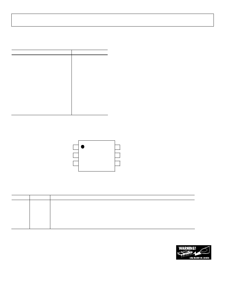
FUNCTIONAL BLOCK DIAGRAM
GND
VCCY
VCCA
A
Y
EN
Figure 1.
GENERAL DESCRIPTION
The ADG3301 is a single channel bidirectional logic level
translator. It can be used in multivoltage digital system
applications such as data transfer between a low voltage
DSP/controller and a higher voltage device. The internal
architecture allows the device to perform bidirectional logic
level translation without an additional signal to set the direction
in which the translation takes place.
The voltage applied to V
CCA
sets the logic levels on the A side of
the device, while V
CCY
sets the levels on the Y side. For proper
operation, V
CCA
must always be less than V
CCY
. The V
CCA-
compatible logic signals applied to the A pin appear as V
CCY
-
compatible levels on the Y pin. Similarly, V
CCY
-compatible logic
levels applied to the Y pin appear as V
CCA
-compatible logic
levels on the A pin.
The enable pin (EN) provides three-state operation on both the
A-side and the Y-side pins. When the device enable pin is pulled
low, the terminals on both sides of the device are in the high
impedance state. The EN pin is referred to the V
CCA
supply
voltage and driven high for normal operation.
The ADG3301 is available in compact 6 lead SC70 package and
is guaranteed to operate over the 1.15 V to 5.5 V supply voltage
range and extended -40°C to +85°C temperature range.
PRODUCT HIGHLIGHTS
1. Bidirectional
level
translation.
2. Fully guaranteed over the 1.15 V to 5.5 V supply range.
3. No direction pin.
4. Compact 6 lead SC70 package.

ADG3301
Preliminary Technical Data
Rev. Pr.A | Page 2 of 18
TABLE OF CONTENTS
Specifications..................................................................................... 3
Absolute Maximum Ratings............................................................ 6
Pin Configurations and Function Descriptions ....................... 6
ESD Caution.................................................................................. 6
Typical Performance Characteristics ............................................. 7
Test Circuits..................................................................................... 11
Terminology .................................................................................... 14
Theory of Operation ...................................................................... 15
Level Translator Architecture ................................................... 15
Input Driving Requirements..................................................... 15
Output Load Requirements ...................................................... 15
Enable Operation ....................................................................... 15
Power Supplies ............................................................................ 15
Data Rate ..................................................................................... 16
Applications..................................................................................... 17
Layout Guidelines....................................................................... 17
Outline Dimensions ....................................................................... 18
Preliminary Technical Data
ADG3301
Rev. Pr.A| Page 3 of 18
SPECIFICATIONS
1
V
CCY
= 1.65 V to 5.5 V, V
CCA
= 1.15 V to V
CCY
, GND = 0 V. All specifications T
MIN
to T
MAX
, unless otherwise noted.
Table 1.
Parameter Symbol
Conditions
Min
Typ
2
Max Unit
LOGIC INPUTS/OUTPUTS
A Side
Input High Voltage
3
V
IHA
V
CCA
= 1.15 V
V
CCA
- 0.3
V
V
IHA
V
CCA
= 1.2 V to 5.5 V
V
CCA
- 0.4
Input Low Voltage
3
V
ILA
0.4
V
Output High Voltage
V
OHA
V
Y
= V
CCY
, I
OH
= 20 µA, Figure 27
V
CCA
- 0.4
V
Output Low Voltage
V
OLA
V
Y
= 0 V, I
OL
= 20 µA, Figure 27
0.4
V
Capacitance
3
C
A
f = 1 MHz, EN = 0, Figure 32
9
pF
Leakage Current
I
LA, HiZ
V
A
= 0 V/V
CCA
, EN = 0, Figure 29
±1
µA
Y Side
Input Low Voltage
3
V
IHY
V
CCY
- 0.4
V
Input High Voltage
3
V
ILY
0.4
V
Output High Voltage
V
OHY
V
A
= V
CCA
, I
OH
= 20 µA, Figure 28
V
CCY
- 0.4
V
Output Low Voltage
V
OLY
V
A
= 0 V, I
OL
= 20 µA, Figure 28
0.4
V
Capacitance
3
C
Y
f = 1 MHz, EN = 0, Figure 33
6
pF
Leakage Current
I
LY, HiZ
V
Y
= 0 V/V
CCY
, EN = 0, Figure 30
±1
µA
Enable (EN)
Input High Voltage
3
V
IHEN
V
CCA
= 1.15 V
V
CCA
- 0.3
V
V
IHEN
V
CCA
= 1.2 V to 5.5 V
V
CCA
- 0.4
V
Input Low Voltage
3
V
ILEN
0.4
V
Leakage Current
I
LEN
V
EN
= 0 V/V
CCA
, V
A
= 0 V, Figure 31
±1
µA
Capacitance
3
C
EN
3
pF
Enable Time
3
t
EN
R
S
= R
T
= 50 , V
A
= 0 V/V
CCA
(A
Y),
V
Y
= 0 V/V
CCY
(Y
A), Figure 34
1
1.8
µs
SWITCHING CHARACTERISTICS
3
3.3 V ± 0.3V
V
CCA
V
CCY,
, V
CCY
= 5 V ± 0.5 V
A
Y Level Translation
R
S
= R
T
= 50 , C
L
= 50 pF, Figure 35
Propagation Delay
t
P, A-Y
6
10
ns
Rise Time
t
R, A-Y
2 3.5 ns
Fall Time
t
F, A-Y
2 3.5 ns
Maximum Data Rate
D
MAX, A-Y
50
Mbps
Channel-to-Channel Skew
t
SKEW, A-Y
2 4
ns
Part-to-Part Skew
t
PPSKEW, A-Y
3
ns
Y
A Level Translation
R
S
= R
T
= 50 , C
L
= 15 pF, Figure 36
Propagation Delay
t
P, Y-A
4
7
ns
Rise Time
t
R, Y-A
1 3 ns
Fall Time
t
F, Y-A
3 7 ns
Maximum Data Rate
D
MAX, Y-A
50
Mbps
Channel-to-Channel Skew
t
SKEW, Y-A
2 3.5 ns
Part-to-Part Skew
t
PPSKEW, Y-A
2
ns
1.8 V ± 0.15 V
V
CCA
V
CCY
, V
CCY
= 3.3 V ± 0.3 V
A
Y Translation
R
S
= R
T
= 50 , C
L
= 50 pF, Figure 35
Propagation Delay
t
P, A-Y
8
11
ns
Rise Time
t
R, A-Y
2 5 ns
Fall Time
t
F, A-Y
2 5 ns
Maximum Data Rate
D
MAX, A-Y
50
Mbps
Channel-to-Channel Skew
t
SKEW, A-Y
2 4
ns
Part-to-Part Skew
t
PPSKEW, A-Y
4
ns
ADG3301
Preliminary Technical Data
Rev. Pr.A | Page 4 of 18
Parameter Symbol
Conditions
Min
Typ
2
Max Unit
Y
A Translation
R
S
= R
T
= 50 , C
L
= 15 pF, Figure 36
Propagation Delay
t
P, Y-A
5
8
ns
Rise Time
t
R, Y-A
2 3.5 ns
Fall Time
t
F, Y-A
2 3.5 ns
Maximum Data Rate
D
MAX, Y-A
50
Mbps
Channel-to-Channel Skew
t
SKEW, Y-A
2 3
ns
Part-to-Part Skew
t
PPSKEW, Y-A
3
ns
1.15 V to 1.3 V
V
CCA
V
CCY
, V
CCY
= 3.3 V ± 0.3 V
A
Y Translation
R
S
= R
T
= 50 , C
L
= 50 pF, Figure 35
Propagation Delay
t
P, A-Y
9
18
ns
Rise Time
t
R, A-Y
3 5 ns
Fall Time
t
F, A-Y
2 5 ns
Maximum Data Rate
D
MAX, A-Y
40
Mbps
Channel-to-Channel Skew
t
SKEW, A-Y
2 5
ns
Part-to-Part Skew
t
PPSKEW, A-Y
10
ns
Y
A Translation
R
S
= R
T
= 50 , C
L
= 15 pF, Figure 36
Propagation Delay
t
P, Y-A
5
9
ns
Rise Time
t
R, Y-A
2 4 ns
Fall Time
t
F, Y-A
2 4 ns
Maximum Data Rate
D
MAX, Y-A
40
Mbps
Channel-to-Channel Skew
t
SKEW, Y-A
2 4
ns
Part-to-Part Skew
t
PPSKEW, Y-A
4
ns
1.15 V to 1.3 V
V
CCA
V
CCY
, V
CCY
= 1.8 V ± 0.3 V
A
Y Translation
R
S
= R
T
= 50 , C
L
= 50 pF, Figure 35
Propagation Delay
t
P, A-Y
12
25
ns
Rise Time
t
R, A-Y
7 12 ns
Fall Time
t
F, A-Y
3 5 ns
Maximum Data Rate
D
MAX, A-Y
25
Mbps
Channel-to-Channel Skew
t
SKEW, A-Y
2 5
ns
Part-to-Part Skew
t
PPSKEW, A-Y
15
ns
Y
A Translation
R
S
= R
T
= 50 , C
L
= 15 pF, Figure 36
Propagation Delay
t
P, Y-A
14
35
ns
Rise Time
t
R, Y-A
5 16 ns
Fall Time
t
F, Y-A
2.5
6.5 ns
Maximum Data Rate
D
MAX, Y-A
25
Mbps
Channel-to-Channel Skew
t
SKEW, Y-A
3 6.5 ns
Part-to-Part Skew
t
PPSKEW, Y-A
23.5 ns
2.5 V ± 0.2 V
V
CCA
V
CCY
, V
CCY
= 3.3 V ± 0.3 V
A
Y Translation
R
S
= R
T
= 50 , C
L
= 50 pF, Figure 35
Propagation Delay
t
P, A-Y
7
10
ns
Rise Time
t
R, A-Y
2.5
4 ns
Fall Time
t
F, A-Y
2 5 ns
Maximum Data Rate
D
MAX, A-Y
60
Mbps
Channel-to-Channel Skew
t
SKEW, A-Y
1.5 2
ns
Part-to-Part Skew
t
PPSKEW, A-Y
4
ns
Y
A Translation
R
S
= R
T
= 50 , C
L
= 15 pF, Figure 36
Propagation Delay
t
P, Y-A
5
8
ns
Rise Time
t
R, Y-A
1 4 ns
Fall Time
t
F, Y-A
3 5 ns
Maximum Data Rate
D
MAX, Y-A
60
Mbps
Channel-to-Channel Skew
t
SKEW, Y-A
2 3
ns
Part-to-Part Skew
t
PPSKEW, Y-A
3
ns
Preliminary Technical Data
ADG3301
Rev. Pr.A| Page 5 of 18
Parameter Symbol
Conditions
Min
Typ
2
Max Unit
POWER REQUIREMENTS
Power Supply Voltages
V
CCA
V
CCA
V
CCY
1.15 5.5
V
V
CCY
1.65 5.5
V
Quiescent Power Supply Current
I
CCA
V
A
= 0 V/V
CCA
,V
Y
= 0 V/V
CCY
,
V
CCA
= V
CCY
= 5.5 V, EN = 1
0.17
1
µA
I
CCY
V
A
= 0 V/V
CCA
, V
Y
= 0 V/V
CCY
,
V
CCA
= V
CCY
= 5.5 V, EN = 1
0.27
1
µA
Three-State Mode Power Supply Current
I
HiZA
V
CCA
= V
CCY
= 5.5 V, EN = 0
0.1
1
µA
I
HiZY
V
CCA
= V
CCY
= 5.5 V, EN = 0
0.1
1
µA
1
Temperature range is a follows: B version: -40°C to +85°C.
2
All typical values are at T
A
= 25°C, unless otherwise noted.
3
Guaranteed by design; not subject to production test.
ADG3301
Preliminary Technical Data
Rev. Pr.A | Page 6 of 18
ABSOLUTE MAXIMUM RATINGS
T
A
= 25°C, unless otherwise noted.
Table 2.
Parameter Rating
V
CCA
to GND
-0.3 V to +7 V
V
CCY
to GND
V
CCA
to +7 V
Digtal Inputs (A)
-0.3 V to (V
CCA
+ 0.3 V)
Digtal Inputs (Y)
-0.3 V to (V
CCY
+ 0.3 V)
EN to GND
-0.3 V to +7 V
Operating Temperature Range
Industrial (B Version)
-40°C to +85°C
Storage Temperature Range
-65°C to +150°C
Junction Temperature
150°C
JA
Thermal Impedance (4-Layer Board)
6 Lead SC70
332
0
C/W
Lead Temperature, Soldering (10 sec)
300°C
IR Reflow, Peak Temperature (< 20 sec)
260°C
Stresses above those listed under Absolute Maximum Ratings
may cause permanent damage to the device. This is a stress
rating only; functional operation of the device at these or any
other conditions above those listed in the operational sections
of this specification is not implied. Exposure to absolute
maximum rating conditions for extended periods may affect
device reliability. Only one absolute maximum rating may be
applied at any one time.
PIN CONFIGURATIONS AND FUNCTION DESCRIPTIONS
GND
EN
ADG3301
TOP VIEW
(Not to Scale)
VCCA
A1
1
2
3
6 VCCY
4
5 Y1
Figure 2. 6-Lead SC70
Table 3 Pin Function Descriptions
Pin No.
Mnemonic
Description
1 V
CCA
Power Supply Voltage Input for the A I/O Pin (1.15 V V
CCA
V
CCY
).
2 A
Input/Output A. Referenced to V
CCA
.
3 GND
Ground.
4
EN
Active High Enable input.
5
Y
Input/Output A4. Referenced to V
CCA
.
6 V
CCY
Power Supply Voltage Input for the Y I/O Pin (1.65 V V
CCY
5.5V).
ESD CAUTION
ESD (electrostatic discharge) sensitive device. Electrostatic charges as high as 4000 V readily accumulate on
the human body and test equipment and can discharge without detection. Although this product features
proprietary ESD protection circuitry, permanent damage may occur on devices subjected to high energy
electrostatic discharges. Therefore, proper ESD precautions are recommended to avoid performance
degradation or loss of functionality.
Preliminary Technical Data
ADG3301
Rev. Pr.A| Page 7 of 18
TYPICAL PERFORMANCE CHARACTERISTICS
Figure 3. I
CCA
vs. Data Rate (A
Y Level Translation)
Figure 4. I
CCY
vs. Data Rate (A
Y Level Translation)
Figure 5. I
CCA
vs. Data Rate (Y
A Level Translation)
Figure 6. I
CCY
vs. Data Rate (Y
A Level Translation)
Figure 7. I
CCY
vs. Capacitive Load at Pin Y for A
Y (1.2 V1.8 V)
Level Translation
Figure 8. I
CCA
vs. Capacitive Load at Pin A for Y
A (1.8 V1.2 V)
Level Translation
ADG3301
Preliminary Technical Data
Rev. Pr.A | Page 8 of 18
Figure 9. I
CCY
vs. Capacitive Load at Pin Y for A
Y (1.8 V3.3 V)
Level Translation
Figure 10.I
CCA
vs. Capacitive Load at Pin A for Y
A (3.3 V1.8 V) Level
Translation
Figure 11. I
CCY
vs. Capacitive Load at Pin Y for A
Y (3.3 V5 V)
Level Translation
Figure 12. I
CCA
vs. Capacitive Load at Pin A for Y
A (5 V3.3 V)
Level Translation
Figure 13. Rise Time vs. Capacitive Load at Pin Y (A
Y Level Translation)
Figure 14. Fall Time vs. Capacitive Load at Pin Y (A
Y Level Translation)
Preliminary Technical Data
ADG3301
Rev. Pr.A| Page 9 of 18
Figure 15. Rise Time vs. Capacitive Load at Pin A (Y
A Level Translation)
Figure 16. Fall Time vs. Capacitive Load at Pin A (Y
A Level Translation)
Figure 17. Propagation Delay (t
PLH
) vs.
Capacitive Load at Pin Y (A
Y Level Translation)
Figure 18. Propagation Delay (t
PHL
) vs.
Capacitive Load at Pin Y (A
Y Level Translation)
Figure 19. Propagation Delay (t
PLH
) vs.
Capacitive Load at Pin A (Y
A Level Translation)
Figure 20. Propagation Delay (t
PHL
) vs.
Capacitive Load at Pin A (Y
A Level Translation)
ADG3301
Preliminary Technical Data
Rev. Pr.A | Page 10 of 18
Figure 21. Eye Diagram at Y Output (1.2 V to 1.8 V Level Translation, 25 Mbps)
Figure 22. Eye Diagram at A Output (1.8 V to 1.2 V Level Translation, 25 Mbps)
Figure 23. Eye Diagram at Y Output (1.8 V to 3.3 V Level Translation, 50 Mbps)
Figure 24. Eye Diagram at A Output (3.3 V to 1.8 V Level Translation, 50 Mbps)
Figure 25. Eye Diagram at Y Output (3.3 V to 5 V Level Translation, 50 Mbps)
Figure 26. Eye Diagram at A Output (5 V to 3.3 V Level Translation, 50 Mbps)
Preliminary Technical Data
ADG3301
Rev. Pr.A| Page 11 of 18
TEST CIRCUITS
ADG3301
A
Y
GND
VCCA
VCCY
0.1
µF
0.1
µF
EN
K1
K2
IOH
IOL
Figure 27. V
OH
/V
OL
Voltages at Pin A
ADG3301
A
Y
GND
VCCA
VCCY
0.1
µF
0.1
µF
EN
K1
K2
IOH
IOL
Figure 28. V
OH
/V
OL
Voltages at Pin Y
ADG3301
A
Y
GND
VCCA
VCCY
0.1
µF
0.1
µF
EN
A
K
Figure 29. Three-State Leakage Current at Pin A
ADG3301
A
Y
GND
VCCA
VCCY
0.1
µF
0.1
µF
EN
A
K
Figure 30. Three-State Leakage Current at Pin Y
ADG3301
A
Y
GND
VCCA
VCCY
0.1
µF
0.1
µF
EN
A
K
Figure 31. EN Pin Leakage Current
ADG3301
A
Y
GND
VCCA
VCCY
EN
Capacitance
Meter
Figure 32. Capacitance at Pin A
ADG3301
Preliminary Technical Data
Rev. Pr.A | Page 12 of 18
ADG3301
A
Y
GND
VCCA
VCCY
EN
Capacitance
Meter
Figure 33. Capacitance at Pin Y
ADG3301
Signal source
RS
RT
Z0=50
A
Y
GND
VCCA
VCCY
0.1
µF
0.1
µF
50pF
VEN
VY
EN
K1
VA
1M
1M
1M
10µF
10µF
ADG3301
Signal source
RS
RT
Z0=50
A
Y
GND
VCCA
VCCY
0.1
µF
0.1
µF
VEN
VY
EN
K1
VA
15pF
1M
1M
10µF
10µF
A-Y direction
Y-A direction
90%
VEN
VY/VA
tEN1
VA/VY
VCCY
0V
VCCA/VCCY
0V
VCCY/VCCA
0V
10%
VEN
VY/VA
tEN2
VA/VY
VCCY
0V
0V
VCCY/VCCA
0V
Note: tEN is whichever is larger between tEN1 and tEN2 in either A->Y and Y->A directions
VCCA/VCCY
Figure 34. Enable Time
Preliminary Technical Data
ADG3301
Rev. Pr.A| Page 13 of 18
ADG3301
Signal source
RS
RT
Z0=50
A
Y
GND
VCCA
VCCY
0.1
µF
0.1
µF
50pF
50%
50%
10%
90%
VA
VY
VA
VY
EN
tF,A-Y
tR,A-Y
tP,A-Y
tP,A-Y
10
µF
10
µF
Figure 35. Switching Characteristics (A
Y Level Translation)
ADG3301
Signal source
RS
RT
Z0=50
A
Y
GND
VCCA
VCCY
0.1
µF
0.1
µF
50%
50%
10%
10%
VA
VY
VY
VA
EN
tF,Y-A
tR,Y-A
tP,Y-A
tP,Y-A
15pF
10
µF
10
µF
Figure 36. Switching Characteristics (Y
A Level Translation)
ADG3301
Preliminary Technical Data
Rev. Pr.A | Page 14 of 18
TERMINOLOGY
Table 4.
Symbol Description
V
IHA
Logic input high voltage at Pin A.
V
ILA
Logic input low voltage at Pin A.
V
OHA
Logic output high voltage at Pin A.
V
OLA
Logic output low voltage at Pin A.
C
A
Capacitance measured at Pin A (EN = 0).
I
LA, HiZ
Leakage current at Pin A when EN = 0 (Pin A three-stated).
V
IHY
Logic input high voltage at Pin Y.
V
ILY
Logic input low voltage at Pin Y.
V
OHY
Logic output high voltage at Pin Y.
V
OLY
Logic output low voltage at Pin Y.
C
Y
Capacitance measured at Pin Y (EN = 0).
I
LY, HiZ
Leakage current at Pin Y when EN = 0 (Pin Y three-stated).
V
IHEN
Logic input high voltage at the EN pin.
V
ILEN
Logic input low voltage at the EN pin.
C
EN
Capacitance measured at EN pin.
I
LEN
Enable (EN) pin leakage curent.
t
EN
Three-state enable time for Pins A /Y.
t
P, A-Y
Propagation delay when translating logic levels in the A
Y direction.
t
R, A-Y
Rise time when translating logic levels in the A
Y direction.
t
F, A-Y
Fall time when translating logic levels in the A
Y direction.
D
MAX, A-Y
Guaranteed data rate when translating logic levels in the A
Y direction under the driving and loading conditions
specified in Table 1.
t
SKEW, A-Y
Difference between propagation delays on any two channels when translating logic levels in the A
Y direction.
t
PPSKEW, A-Y
Difference in propagation delay between any one channel and the same channel on a different part (under same
driving/loading conditions) when translating in the A
Y direction.
t
P, Y-A
Propagation delay when translating logic levels in the Y
A direction.
t
R, Y-A
Rise time when translating logic levels in the Y
A direction.
t
F, Y-A
Fall time when translating logic levels in the Y
A direction.
D
MAX, Y-A
Guaranteed data rate when translating logic levels in the Y
A direction under the driving and loading conditions
specified in Table 1.
t
SKEW, Y-A
Difference between propagation delays on any two channels when translating logic levels in the Y
A direction.
t
PPSKEW, Y-A
Difference in propagation delay between any one channel and the same channel on a different part (under same
driving/loading conditions) when translating in the Y
A direction.
V
CCA
Power supply voltage at the V
CCA
pin.
V
CCY
Power supply voltage at the V
CCY
pin.
I
CCA
V
CCA
supply current.
I
CCY
V
CCY
supply current.
I
HiZA
V
CCA
supply current during three-state mode (EN = 0).
I
HiZY
V
CCY
supply current during three-state mode (EN = 0).
Preliminary Technical Data
ADG3301
Rev. Pr.A| Page 15 of 18
THEORY OF OPERATION
The ADG3301 level translator allows the level shifting
necessary for data transfer in a system where multiple supply
voltages are used. The device requires two supplies, V
CCA
and
V
CCY
(V
CCA
V
CCY
). These supplies set the logic levels on each
side of the device. When driving the A pin, the device translates
the V
CCA
compatible logic levels to V
CCY
compatible logic levels
available at the Y pin. Similarly, since the device is capable of
bidirectional translation, when driving the Y pin the V
CCY
compatible logic levels are translated to V
CCA
-compatible logic
levels available at the A pin. When EN = 0, the A and Y pins are
three-stated. When EN is driven high, the ADG3301 goes into
normal operation mode and performs level translation.
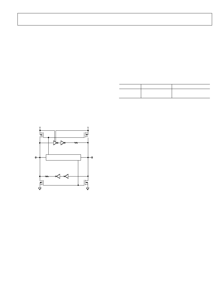
LEVEL TRANSLATOR ARCHITECTURE
The ADG3301 consists of a single bidirectional channel that can
translate logic levels in either the A
Y or the Y
A direction. It
uses a one-shot accelerator architecture, which ensures excellent
switching characteristics. Figure 37 shows a simplified block
diagram of the ADG3301 level translator.
ONE-SHOT GENERATOR
6k
6k
Y
V
CCA
V
CCY
T2
T1
T3
T4
A
04860-053
P
N
U1
U2
U4
U3
Figure 37. Simplified Block Diagram of an ADG3301 Channel
The logic level translation in the A
Y direction is performed
using a level translator (U1) and an inverter (U2), while the
translation in the Y
A direction is performed using the
inverters U3 and U4. The one-shot generator detects a rising or
falling edge present on either the A side or the Y side of the
channel. It sends a short pulse that turns on the PMOS
transistors (T1T2) for a rising edge, or the NMOS transistors
(T3T4) for a falling edge. This charges/discharges the capacitive
load faster, which results in fast rise and fall times.
INPUT DRIVING REQUIREMENTS
To ensure correct operation of the ADG3301, the circuit that
drives the input of an ADG3301 channels must have an output
impedance of less than or equal to 150 and a minimum peak
current driving capability of 36 mA.
OUTPUT LOAD REQUIREMENTS
The ADG3301 level translator is designed to drive CMOS-
compatible loads. If current driving capability is required, it is
recommended to use buffers between the ADG3301 outputs
and the load.
ENABLE OPERATION
The ADG3301 provides three-state operation at the A and Y
I/O pins by using the enable (EN) pin as shown in Table 5.
Table 5. Truth Table
EN
Y I/O Pin
A I/O Pin
0 Hi-Z
1
Hi-Z
1
1 Normal
operation
2
Normal operation
2
1
High impedance state.
2
In normal operation, the ADG3301 performs level translation.
While EN = 0, the ADG3301 enters into tri-state mode. In this
mode, the current consumption from both the V
CCA
and V
CCY
supplies is reduced, allowing the user to save power, which is
critical, especially on battery-operated systems. The EN input
pin can be driven with either V
CCA
- or V
CCY
-compatible logic
levels.
POWER SUPPLIES
For proper operation of the ADG3301, the voltage applied to
the V
CCA
must be always less than or equal the voltage applied to
V
CCY
. To meet this condition, the recommended power-up
sequence is V
CCY
first and then V
CCA
. The ADG3301 operates
properly only after both supply voltages reach their nominal
values. It is not recommended to use the part in a system where,
during power-up, V
CCA
may be greater than V
CCY
due to
significant increase in the current taken from the V
CCA
supply
For optimum performance, the V
CCA
and V
CCY
pins should be
decoupled to GND, and placed as close as possible to the device.
ADG3301
Preliminary Technical Data
Rev. Pr.A | Page 16 of 18
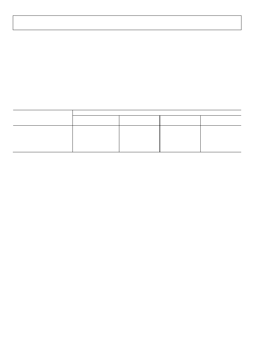
DATA RATE
The maximum data rate at which the device is guaranteed to
operate is a function of the V
CCA
and V
CCY
supply voltage
combination and the load capacitance. It is given by the
maximum frequency of a square wave that can be applied to the
device, which meets the V
OH
and V
OL
levels at the output and
does not exceed the maximum junction temperature (see the
Absolute Maximum Ratings).Table 6 shows the guaranteed
data rates at which the ADG3301 can operate in both directions
(A
Y or Y
A level translation) for various V
CCA
and V
CCY
supply combinations.
Table 6. Guaranteed Data Rate (Mbps)
1
V
CCY
V
CCA
1.8 V
(1.65 V to 1.95 V)
2.5 V
(2.3 V to 2.7 V)
3.3 V
(3.0 V to 3.6 V)
5 V
(4.5 V to 5.5 V)
1.2 V (1.15 V to 1.3 V)
25 30
40
40
1.8 V (1.65 V to 1.95 V)
- 45
50
50
2.5 V (2.3 V to 2.7 V)
- -
60
50
3.3 V (3.0 V to 3.6 V)
- -
-
50
5 V (4.5 V to 5.5 V)
- -
-
-
1
The load capacitance used is 50 pF when translating in the A
Y direction and 15 pF when translating in the YA direction.
Preliminary Technical Data
ADG3301
Rev. Pr.A| Page 17 of 18
APPLICATIONS
The ADG3301 is designed for digital circuits that operate at
different supply voltages; therefore, logic level translation is
required. The lower voltage logic signals are connected to the A
pin, and the higher voltage logic signals to the Y pin. The
ADG3301 can provide level translation in both directions from
A
Y or Y
A, eliminating the need for a level translator IC for
each direction. The internal architecture allows the ADG3301
to perform bidirectional level translation without an additional
signal to set the direction in which the translation is made. It
also allows simultaneous data flow in both directions on the
same part, for example, two channels translate in AY direction
while the other two translate in YA direction. This simplifies
the design by eliminating the timing requirements for the
direction signal and reduces the number of ICs used for level
translation.
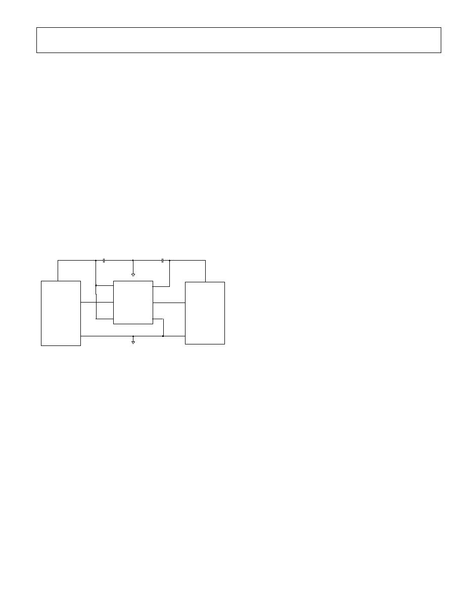
Figure 38 shows an application where a 1.8V microprocessors
transfers data to or from a 3.3V peripheral device using the
ADG3301 level translator.
VCCA
A
EN
GND
Y
VCCY
ADG3301
Microprocessor
/Microcontroller
/DSP
I/OL
I/OH
GND
GND
1.8V
3.3V
100nF
Peripheral
Device
100nF
Figure 39. 1.8V to 3.3V level translation circuit
LAYOUT GUIDELINES
As with any high speed digital IC, the printed circuit board
layout is important for the overall performance of the circuit.
Care should be taken to ensure proper power supply bypass and
return paths for the high speed signals. Each V
CC
pin (V
CCA
and
V
CCY
) should be bypassed using low effective series resistance
(ESR) and effective series inductance (ESI) capacitors placed as
close as possible to the V
CCA
and V
CCY
pins. The parasitic
inductance of the high speed signal track might cause
significant overshoot. This effect can be reduced by keeping the
length of the tracks as short as possible. A solid copper plane for
the return path (GND) is also recommended.
ADG3301
Preliminary Technical Data
Rev. Pr.A | Page 18 of 18
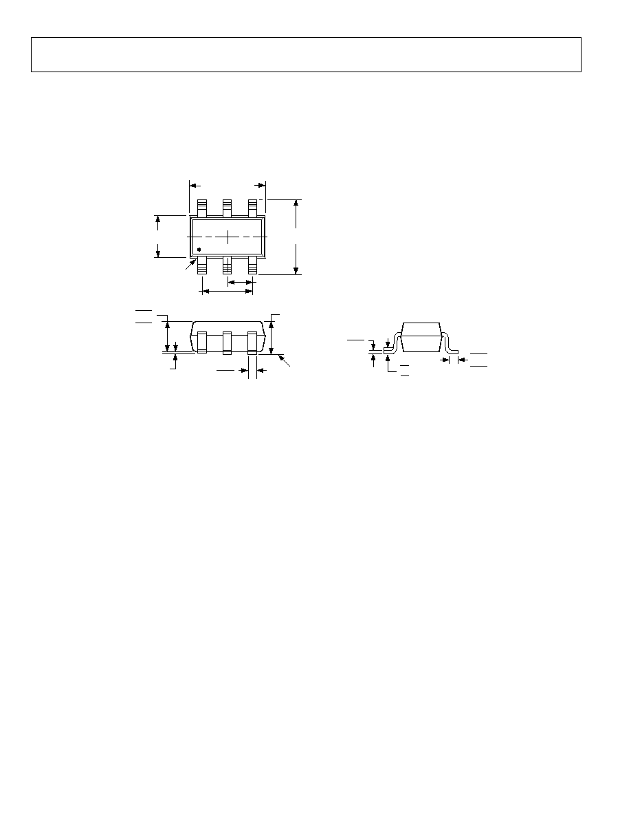
OUTLINE DIMENSIONS
0.22
0.08
0.46
0.36
0.26
8
4
0
0.30
0.15
1.00
0.90
0.70
SEATING
PLANE
1.10 MAX
3
5
4
2
6
1
2.00 BSC
PIN 1
2.10 BSC
0.65 BSC
1.25 BSC
1.30 BSC
0.10 MAX
0.10 COPLANARITY
COMPLIANT TO JEDEC STANDARDS MO-203AB
6-Lead Plastic Surface Mount Package [SC70]
(KS-6)
Dimensions shown in millimeters
Figure 40. 6 Lead SC 70 package
PR05517-0-7/05(PrA)