Äîêóìåíòàöèÿ è îïèñàíèÿ www.docs.chipfind.ru
REV. 0
a
AD9288
One Technology Way, P.O. Box 9106, Norwood, MA 02062-9106, U.S.A.
Tel: 781/329-4700
World Wide Web Site: http://www.analog.com
Fax: 781/326-8703
© Analog Devices, Inc., 1999
Information furnished by Analog Devices is believed to be accurate and
reliable. However, no responsibility is assumed by Analog Devices for its
use, nor for any infringements of patents or other rights of third parties
which may result from its use. No license is granted by implication or
otherwise under any patent or patent rights of Analog Devices.
8-Bit, 40/80/100 MSPS
Dual A/D Converter
FUNCTIONAL BLOCK DIAGRAM
T/H
ADC
REF
T/H
ADC
OUTPUT REGISTER
8
8
8
8
OUTPUT REGISTER
TIMING
TIMING
AD9288
V
DD
D7
A
D0
A
SELECT #1
SELECT #2
DATA FORMAT
SELECT
D7
B
D0
B
ENC
A
A
IN
A
A
IN
A
REF
IN
A
REF
OUT
REF
IN
B
A
IN
B
A
IN
B
ENC
B
V
D
GND
V
DD
FEATURES
Dual 8-Bit, 40 MSPS, 80 MSPS, and 100 MSPS ADC
Low Power: 90 mW at 100 MSPS per Channel
On-Chip Reference and Track/Holds
475 MHz Analog Bandwidth Each Channel
SNR = 47 dB @ 41 MHz
1 V p-p Analog Input Range Each Channel
Single +3.0 V Supply Operation (2.7 V3.6 V)
Standby Mode for Single Channel Operation
Twos Complement or Offset Binary Output Mode
Output Data Alignment Mode
APPLICATIONS
Battery Powered Instruments
Hand-Held Scopemeters
Low Cost Digital Oscilloscopes
I and Q Communications
GENERAL DESCRIPTION
The AD9288 is a dual 8-bit monolithic sampling analog-to-
digital converter with on-chip track-and-hold circuits and is
optimized for low cost, low power, small size and ease of use.
The product operates at a 100 MSPS conversion rate with out-
standing dynamic performance over its full operating range.
Each channel can be operated independently.
The ADC requires only a single 3.0 V (2.7 V to 3.6 V) power
supply and an encode clock for full-performance operation. No
external reference or driver components are required for many
applications. The digital outputs are TTL/CMOS compatible
and a separate output power supply pin supports interfacing
with 3.3 V or 2.5 V logic.
The encode input is TTL/CMOS compatible and the 8-bit
digital outputs can be operated from +3.0 V (2.5 V to 3.6 V)
supplies. User-selectable options are available to offer a combi-
nation of standby modes, digital data formats and digital data
timing schemes. In standby mode, the digital outputs are driven
to a high impedance state.
Fabricated on an advanced CMOS process, the AD9288 is avail-
able in a 48-lead surface mount plastic package (7
×
7 mm,
1.4 mm LQFP) specified over the industrial temperature range
(40
°
C to +85
°
C).

REV. 0
2
AD9288SPECIFICATIONS
Test
AD9288BST-100
AD9288BST-80
AD9288BST-40
Parameter
Temp
Level
Min
Typ
Max
Min
Typ
Max
Min
Typ
Max
Units
RESOLUTION
8
8
8
Bits
DC ACCURACY
Differential Nonlinearity
+25
°
C
I
±
0.5
+1.25
±
0.5
+1.25
±
0.5
+1.25
LSB
Full
VI
+1.50
+1.50
+1.50
LSB
Integral Nonlinearity
+25
°
C
I
±
0.50
+1.25
±
0.50
+1.25
±
0.50
+1.25
LSB
Full
VI
+1.50
+1.50
+1.50
LSB
No Missing Codes
Full
VI
Guaranteed
Guaranteed
Guaranteed
Gain Error
1
+25
°
C
I
6
±
2.5
+6
6
±
2.5
+6
6
±
2.5
+6
% FS
Full
VI
8
+8
8
+8
8
+8
% FS
Gain Tempco
1
Full
VI
80
80
80
ppm/
°
C
Gain Matching
+25
°
C
V
±
1.5
±
1.5
±
1.5
% FS
Voltage Matching
+25
°
C
V
±
15
±
15
±
15
mV
ANALOG INPUT
Input Voltage Range
(With Respect to
AIN)
Full
V
±
512
±
512
±
512
mV p-p
Common-Mode Voltage
Full
V
±
200
±
200
±
200
mV
Input Offset Voltage
+25
°
C
I
35
±
10
+35
35
±
10
+35
35
±
10
+35
mV
Full
VI
±
40
±
40
±
40
mV
Reference Voltage
Full
VI
1.2
1.25
1.3
1.2
1.25
1.3
1.2
1.25
1.3
V
Reference Tempco
Full
VI
±
130
±
130
±
130
ppm/
°
C
Input Resistance
+25
°
C
I
7
10
13
7
10
13
7
10
13
k
Full
VI
5
16
5
16
5
16
k
Input Capacitance
+25
°
C
V
2
2
2
pF
Analog Bandwidth, Full Power
+25
°
C
V
475
475
475
MHz
SWITCHING PERFORMANCE
Maximum Conversion Rate
Full
VI
100
80
40
MSPS
Minimum Conversion Rate
+25
°
C
IV
1
1
1
MSPS
Encode Pulsewidth High (t
EH
)
+25
°
C
IV
4.3
1000
5.0
1000
8.0
1000
ns
Encode Pulsewidth Low (t
EL
)
+25
°
C
IV
4.3
1000
5.0
1000
8.0
1000
ns
Aperture Delay (t
A
)
+25
°
C
V
0
0
0
ns
Aperture Uncertainty (Jitter)
+25
°
C
V
5
5
5
ps rms
Output Valid Time (t
V
)
2
Full
VI
3.0
3.0
3.0
ns
Output Propagation Delay (t
PD
)
2
Full
VI
4.5
4.5
4.5
ns
DIGITAL INPUTS
Logic "1" Voltage
Full
VI
2.0
2.0
2.0
V
Logic "0" Voltage
Full
VI
0.8
0.8
0.8
V
Logic "1" Current
Full
VI
±
1
±
1
±
1
µ
A
Logic "0" Current
Full
VI
±
1
±
1
±
1
µ
A
Input Capacitance
+25
°
C
V
2.0
2.0
2.0
pF
DIGITAL OUTPUTS
3
Logic "1" Voltage
Full
VI
2.45
2.45
2.45
V
Logic "0" Voltage
Full
VI
0.05
0.05
0.05
V
POWER SUPPLY
Power Dissipation
4
Full
VI
180
218
171
207
156
189
mW
Standby Dissipation
4, 5
Full
VI
6
11
6
11
6
11
mW
Power Supply Rejection Ratio
(PSRR)
+25
°
C
I
8
20
8
20
8
20
mV/V
DYNAMIC PERFORMANCE
6
Transient Response
+25
°
C
V
2
2
2
ns
Overvoltage Recovery Time
+25
°
C
V
2
2
2
ns
Signal-to-Noise Ratio (SNR)
(Without Harmonics)
f
IN
= 10.3 MHz
+25
°
C
I
47.5
47.5
44
47.5
dB
f
IN
= 26 MHz
+25
°
C
I
47.5
44
47
dB
f
IN
= 41 MHz
+25
°
C
I
44
47.0
dB
(V
DD
= 3.0 V; V
D
= 3.0 V, Differential Input; External reference unless otherwise noted.)
REV. 0
3
AD9288
Test
AD9288BST-100
AD9288BST-80
AD9288BST-40
Parameter
Temp
Level
Min
Typ
Max
Min
Typ
Max
Min
Typ
Max
Units
DYNAMIC PERFORMANCE
6
(Continued)
Signal-to-Noise Ratio (SINAD) (With Harmonics)
f
IN
= 10.3 MHz
+25
°
C
I
47
47
44
47
dB
f
IN
= 26 MHz
+25
°
C
I
47
44
47
dB
f
IN
= 41 MHz
+25
°
C
I
44
47
47
dB
Effective Number of Bits
f
IN
= 10.3 MHz
+25
°
C
I
7.5
7.5
7.0
7.5
Bits
f
IN
= 26 MHz
+25
°
C
I
7.5
7.0
7.5
Bits
f
IN
= 41 MHz
+25
°
C
I
7.0
7.5
7.5
Bits
2nd Harmonic Distortion
f
IN
= 10.3 MHz
+25
°
C
I
70
70
55
70
dBc
f
IN
= 26 MHz
+25
°
C
I
70
55
70
dBc
f
IN
= 41 MHz
+25
°
C
I
55
70
70
dBc
3rd Harmonic Distortion
f
IN
= 10.3 MHz
+25
°
C
I
60
60
55
60
dBc
f
IN
= 26 MHz
+25
°
C
I
60
55
60
dBc
f
IN
= 41 MHz
+25
°
C
I
52
60
60
dBc
Two-Tone Intermod Distortion (IMD)
f
IN
= 10.3 MHz
+25
°
C
V
60
60
60
dBc
NOTES
1
Gain error and gain temperature coefficient are based on the ADC only (with a fixed 1.25 V external reference).
2
t
V
and t
PD
are measured from the 1.5 V level of the ENCODE input to the 10%/90% levels of the digital outputs swing. The digital output load during test is not to
exceed an ac load of 10 pF or a dc current of
±
40
µ
A.
3
Digital supply current based on V
DD
= +3.0 V output drive with <10 pF loading under dynamic test conditions.
4
Power dissipation measured under the following conditions: f
S
= 100 MSPS, analog input is 0.7 dBFS, both channels in operation.
5
Standby dissipation calculated with encode clock in operation.
6
SNR/harmonics based on an analog input voltage of 0.7 dBFS referenced to a 1.024 V full-scale input range.
Specifications subject to change without notice.
CAUTION
ESD (electrostatic discharge) sensitive device. Electrostatic charges as high as 4000 V readily
accumulate on the human body and test equipment and can discharge without detection.
Although the AD9288 features proprietary ESD protection circuitry, permanent damage may
occur on devices subjected to high energy electrostatic discharges. Therefore, proper ESD
precautions are recommended to avoid performance degradation or loss of functionality.
WARNING!
ESD SENSITIVE DEVICE
ABSOLUTE MAXIMUM RATINGS*
V
D
, V
DD
. . . . . . . . . . . . . . . . . . . . . . . . . . . . . . . . . . . . . . +4 V
Analog Inputs . . . . . . . . . . . . . . . . . . . . 0.5 V to V
D
+ 0.5 V
Digital Inputs . . . . . . . . . . . . . . . . . . . 0.5 V to V
DD
+ 0.5 V
VREF IN . . . . . . . . . . . . . . . . . . . . . . . . 0.5 V to V
D
+ 0.5 V
Digital Output Current . . . . . . . . . . . . . . . . . . . . . . . . 20 mA
Operating Temperature . . . . . . . . . . . . . . . . 55
°
C to +125
°
C
Storage Temperature . . . . . . . . . . . . . . . . . . 65
°
C to +150
°
C
Maximum Junction Temperature . . . . . . . . . . . . . . . +175
°
C
Maximum Case Temperature . . . . . . . . . . . . . . . . . . +150
°
C
*Stresses above those listed under Absolute Maximum Ratings may cause perma-
nent damage to the device. This is a stress rating only; functional operation of the
device at these or any other conditions outside of those indicated in the operation
sections of this specification is not implied. Exposure to absolute maximum
ratings for extended periods may affect device reliability.
EXPLANATION OF TEST LEVELS
Test Level
I
100% production tested.
II
100% production tested at +25
°
C and sample tested at
specified temperatures.
III Sample tested only.
IV Parameter is guaranteed by design and characterization
testing.
V
Parameter is a typical value only.
VI 100% production tested at +25
°
C; guaranteed by design
and characterization testing for industrial temperature
range; 100% production tested at temperature extremes for
military devices.
Table I. User Select Options
S1
S2
User Select Options
0
0
Standby Both Channels A and B.
0
1
Standby Channel B Only.
1
0
Normal Operation (Data Align Disabled).
1
1
Data align enabled (data from both channels avail-
able on rising edge of Clock A. Channel B data is
delayed a 1/2 clock cycle).
ORDERING GUIDE
Temperature
Package
Model
Ranges
Options
AD9288BST
-40, -80, -100
40
°
C to +85
°
C
ST-48*
AD9288/PCB
+25
°
C
Evaluation Board
*ST = Thin Plastic Quad Flatpack (1.4 mm thick, 7
×
7 mm: LQFP).
REV. 0
AD9288
4
PIN CONFIGURATION
36
35
34
33
32
31
30
29
28
27
26
25
13 14 15 16 17 18 19 20 21 22 23 24
1
2
3
4
5
6
7
8
9
10
11
12
D5
A
D1
A
ENC
A
48 47 46 45 44
39 38 37
43 42 41 40
PIN 1
IDENTIFIER
TOP VIEW
(Not to Scale)
NC
NC
V
DD
GND
GND
V
D
V
D
D6
B
ENC
B
GND
V
DD
(MSB) D7
B
D5
B
GND
A
IN
A
A
IN
A
DFS
REF
IN
A
REF
OUT
REF
IN
B
NC = NO CONNECT
S1
S2
A
IN
B
A
IN
B
GND
GND
V
DD
NC
D4
B
D3
B
D2
B
D1
B
D4
A
V
D
V
DD
D7
A
(MSB)
D6
A
D0
A
AD9288
GND
D2
A
D3
A
D0
B
GND
NC
V
D
PIN FUNCTION DESCRIPTIONS
Pin No.
Name
Description
1, 12, 16, 27, 29,
32, 34, 45
GND
Ground.
2
A
IN
A
Analog Input for Channel A.
3
AINA
Analog Input for Channel A
(Complementary).
4
DFS
Data Format Select: (Offset
binary output available if set
low. Twos complement output
available if set high).
5
REF
IN
A
Reference Voltage Input for
Channel A.
6
REF
OUT
Internal Reference Voltage.
7
REF
IN
B
Reference Voltage Input for
Channel B.
8
S1
User Select #1 (Refer to Table
I), Tied with Respect to V
D
.
9
S2
User Select #2 (Refer to Table
I), Tied with Respect to V
D
.
10
AINB
Analog Input for Channel B
(Complementary).
11
A
IN
B
Analog Input for Channel B.
13, 30, 31, 48
V
D
Analog Supply (3 V).
14
ENC
B
Clock Input for Channel B.
15, 28, 33, 46
V
DD
Digital Supply (3 V).
1724
D7
B
D0
B
Digital Output for Channel B.
25, 26, 35, 36
NC
Do Not Connect.
3744
D0
A
D7
A
Digital Output for Channel A.
47
ENC
A
Clock Input for Channel A.
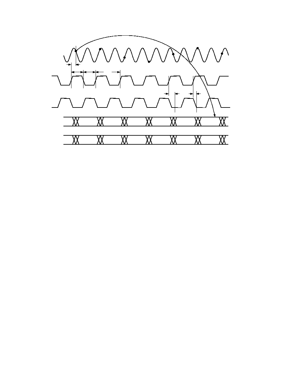
Aperture Delay
The delay between a differential crossing of ENCODE and
ENCODE and the instant at which the analog input is sampled.
Aperture Uncertainty (Jitter)
The sample-to-sample variation in aperture delay.
Differential Nonlinearity
The deviation of any code from an ideal 1 LSB step.
Encode Pulsewidth/Duty Cycle
Pulsewidth high is the minimum amount of time that the EN-
CODE pulse should be left in Logic "1" state to achieve rated
performance; pulsewidth low is the minimum time ENCODE
pulse should be left in low state. At a given clock rate, these
specs define an acceptable Encode duty cycle.
Integral Nonlinearity
The deviation of the transfer function from a reference line
measured in fractions of 1 LSB using a "best straight line" deter-
mined by a least square curve fit.
Minimum Conversion Rate
The encode rate at which the SNR of the lowest analog signal
frequency drops by no more than 3 dB below the guaranteed
limit.
Maximum Conversion Rate
The encode rate at which parametric testing is performed.
Output Propagation Delay
The delay between a differential crossing of ENCODE and
ENCODE and the time when all output data bits are within
valid logic levels.
Power Supply Rejection Ratio
The ratio of a change in input offset voltage to a change in
power supply voltage.
Signal-to-Noise-and-Distortion (SINAD)
The ratio of the rms signal amplitude (set at 1 dB below full
scale) to the rms value of the sum of all other spectral compo-
nents, including harmonics but excluding dc.
Signal-to-Noise Ratio (SNR)
The ratio of the rms signal amplitude (set at 1 dB below full
scale) to the rms value of the sum of all other spectral compo-
nents, excluding the first five harmonics and dc.
Spurious-Free Dynamic Range (SFDR)
The ratio of the rms signal amplitude to the rms value of the
peak spurious spectral component. The peak spurious compo-
nent may or may not be a harmonic. May be reported in dBc
(i.e., degrades as signal levels is lowered), or in dBFS (always
related back to converter full scale).
Two-Tone Intermodulation Distortion Rejection
The ratio of the rms value of either input tone to the rms
value of the worst third order intermodulation product; re-
ported in dBc.
Two-Tone SFDR
The ratio of the rms value of either input tone to the rms value
of the peak spurious component. The peak spurious component
may or may not be an IMD product. May be reported in dBc
(i.e., degrades as signal levels is lowered), or in dBFS (always
related back to converter full scale).
Worst Harmonic
The ratio of the rms signal amplitude to the rms value of the
worst harmonic component, reported in dBc.
DEFINITION OF SPECIFICATIONS
Analog Bandwidth (Small Signal)
The analog input frequency at which the spectral power of the
fundamental frequency (as determined by the FFT analysis) is
reduced by 3 dB.
REV. 0
AD9288
5
A
IN
A, A
IN
B
ENCODE A, B
D7
A
D0
A
SAMPLE N
SAMPLE N+1
SAMPLE N+2
SAMPLE N+3
SAMPLE N+4
t
A
t
V
t
PD
SAMPLE N+5
1/f
S
t
EL
t
EH
DATA N4
DATA N3
DATA N2
DATA N1
DATA N
D7
B
D0
B
DATA N4
DATA N3
DATA N2
DATA N1
DATA N
DATA N+1
DATA N+1
Figure 1. Normal Operation, Same Clock (S1 = 1, S2 = 0) Channel Timing
A
IN
A, A
IN
B
ENCODE A
D7
A
D0
A
SAMPLE N
SAMPLE N+1
SAMPLE N+2
SAMPLE N+3
SAMPLE N+4
t
A
t
V
t
PD
SAMPLE N+5
1/f
S
t
EL
t
EH
DATA N4
DATA N3
DATA N2
DATA N1
DATA N
D7
B
D0
B
DATA N4
DATA N3
DATA N2
DATA N1
DATA N
DATA N+1
ENCODE B
DATA N+1
Figure 2. Normal Operation with Two Clock Sources (S1 = 1, S2 = 0) Channel Timing
REV. 0
AD9288
6
A
IN
A, A
IN
B
ENCODE A
D7
A
D0
A
SAMPLE N
SAMPLE N+1
SAMPLE N+2
SAMPLE N+3
SAMPLE N+4
t
A
t
V
t
PD
SAMPLE N+5
1/f
S
t
EL
t
EH
DATA N4
DATA N3
DATA N2
DATA N1
DATA N
D7
B
D0
B
DATA N4
DATA N3
DATA N2
DATA N1
DATA N
DATA N+1
ENCODE B
DATA N+1
Figure 3. Data Align with Two Clock Sources (S1 = 1, S2 = 1) Channel Timing
REV. 0
SAMPLE
0
dB
10
20
30
40
50
60
70
80
90
ENCODE = 100MSPS
A
IN
= 10.3MHz
SNR = 48.52dB
SINAD = 48.08dB
2ND HARMONIC = 62.54dBc
3RD HARMONIC = 63.56dBc
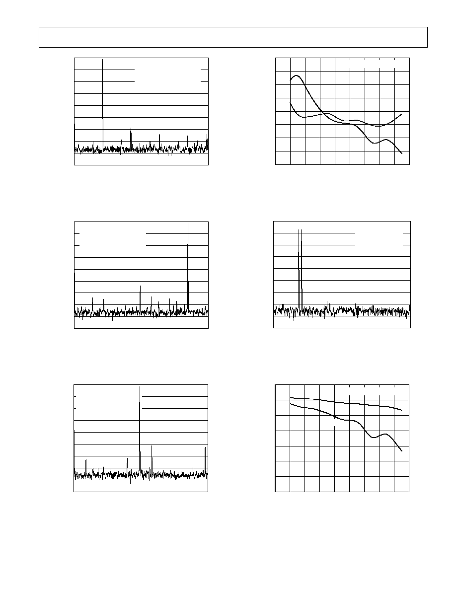
Figure 4. Spectrum: f
S
= 100 MSPS, f
IN
= 10 MHz,
Single-Ended Input
SAMPLE
0
dB
10
20
30
40
50
60
70
80
90
ENCODE = 100MSPS
A
IN
= 41MHz
SNR = 47.87dB
SINAD = 46.27dB
2ND HARMONIC = 54.10dBc
3RD HARMONIC = 55.46dBc
Figure 5. Spectrum: f
S
= 100 MSPS, f
IN
= 41 MHz,
Single-Ended Input
SAMPLE
0
dB
10
20
30
40
50
60
70
80
90
ENCODE = 100MSPS
A
IN
= 76MHz
SNR = 47.1dB
SINAD = 43.2dB
2ND HARMONIC = 52.2dBc
3RD HARMONIC = 51.5dBc
Figure 6. Spectrum: f
S
= 100 MSPS, f
IN
= 76 MHz,
Single-Ended Input
MHz
72.00
dB
68.00
64.00
60.00
56.00
52.00
48.00
44.00
40.00
10
20
30
40
50
60
70
80
90
ENCODE RATE = 100MSPS
2ND
3RD
0
Figure 7. Harmonic Distortion vs. A
IN
Frequency
SAMPLE
0
dB
10
20
30
40
50
60
70
80
90
ENCODE = 100MSPS
A
IN
1 = 9.3MHz
A
IN
2 = 10.3MHz
IMD = 60.0dBc
Figure 8. Two-Tone Intermodulation Distortion
MHz
50.00
dB
48.00
46.00
44.00
42.00
40.00
38.00
36.00
10
20
30
40
50
60
70
80
90
ENCODE RATE = 100MSPS
SNR
SINAD
0
Figure 9. SINAD/SNR vs. A
IN
Frequency
Typical Performance CharacteristicsAD9288
7
REV. 0
AD9288
8
MSPS
49.00
dB
48.00
47.00
46.00
45.00
30
40
50
60
70
80
90
100
110
A
IN
= 10.3MHz
SINAD
SNR
Figure 10. SINAD/SNR vs. Encode Rate
ENCODE HIGH PULSEWIDTH ns
50.00
dB
46.00
42.00
38.00
30.00
7.0
6.5
6.0
5.5
5.0
4.5
4.0
3.5
3.0
A
IN
= 10.3MHz
SINAD
34.00
SNR
Figure 11. SINAD/SNR vs. Encode Pulsewidth High
BANDWIDTH MHz
0.5
dB
0.0
0.5
1.0
2.0
0
100
200
300
400
500
600
1.5
ENCODE RATE = 100MSPS
2.5
3.0
3.5
4.0
4.5
5.0
5.5
3dB
Figure 12. ADC Frequency Response: f
S
= 100 MSPS
MSPS
190
POWER mW
185
180
175
170
10
20
30
40
50
60
70
80
90
A
IN
= 10.3MHz
165
160
155
150
145
140
100
0
Figure 13. Analog Power Dissipation vs. Encode Rate
TEMPERATURE C
48.0
dB
47.5
47.0
46.5
46.0
40
25
85
45.5
45.0
44.5
44.0
43.5
SNR
SINAD
ENCODE RATE = 100MSPS
A
IN
= 10.3MHz
Figure 14. SINAD/SNR vs. Temperature
TEMPERATURE C
0.6
% GAIN
0.4
0.2
0
0.2
40
25
85
0.4
0.6
0.8
1.0
ENCODE RATE = 100MSPS
A
IN
= 10.3MHz
Figure 15. ADC Gain vs. Temperature (with External
+1.25 V Reference)
REV. 0
AD9288
9
CODE
2.0
LSB
0.5
1.0
1.5
2.0
0.5
0.0
1.0
1.5
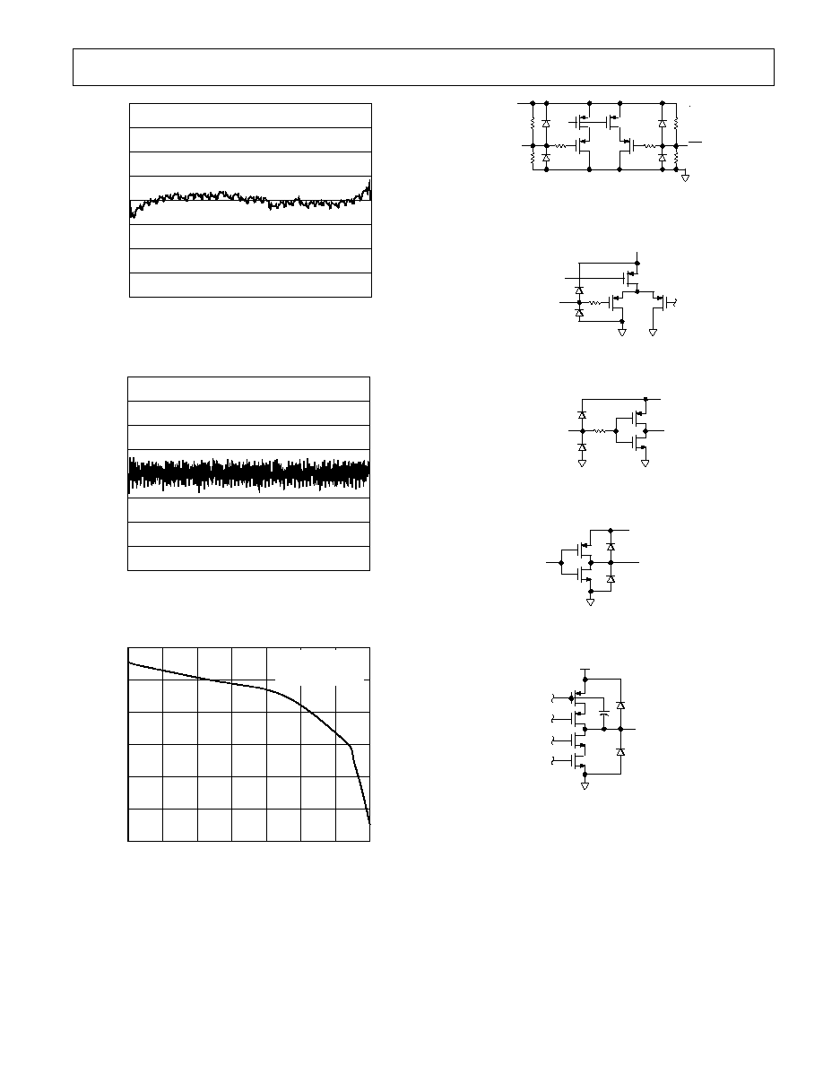
Figure 16. Integral Nonlinearity
CODE
1.00
0.75
LSB
0.25
0.50
0.75
1.00
0.25
0.00
0.50
Figure 17. Differential Nonlinearity
LOAD mA
1.3
V
REFOUT
V
1.2
1.1
1.0
0
0.9
0.8
0.7
ENCODE = 100MSPS
V
D
= 3.0V
T
A
= +25 C
0.25
0.5
0.75
1
1.25
1.5
1.75
Figure 18. Voltage Reference Out vs. Current Load
A
IN
A
IN
28k
12k
28k
12k
V
D
Figure 19. Equivalent Analog Input Circuit
V
BIAS
REF
IN
V
D
Figure 20. Equivalent Reference Input Circuit
V
D
ENCODE
Figure 21. Equivalent Encode Input Circuit
V
DD
OUT
Figure 22. Equivalent Digital Output Circuit
V
D
OUT
Figure 23. Equivalent Reference Output Circuit

REV. 0
AD9288
10
APPLICATION NOTES
THEORY OF OPERATION
The AD9288 ADC architecture is a bit-per-stage pipeline-type
converter utilizing switch capacitor techniques. These stages
determine the 5 MSBs and drive a 3-bit flash. Each stage pro-
vides sufficient overlap and error correction allowing optimiza-
tion of comparator accuracy. The input buffers are differential
and both sets of inputs are internally biased. This allows the
most flexible use of ac or dc and differential or single-ended
input modes. The output staging block aligns the data, carries
out the error correction and feeds the data to output buffers.
The set of output buffers are powered from a separate supply,
allowing adjustment of the output voltage swing. There is no
discernible difference in performance between the two channels.
USING THE AD9288
Good high speed design practices must be followed when using
the AD9288. To obtain maximum benefit, decoupling capacitors
should be physically as close to the chip as possible, minimizing
trace and via inductance between chip pins and capacitor (0603
surface mount caps are used on the AD9288/PCB evaluation
board). It is recommended to place a 0.1
µ
F capacitor at each
power-ground pin pair for high frequency decoupling, and in-
clude one 10
µ
F capacitor for local low frequency decoupling.
The VREF IN pin should also be decoupled by a 0.1
µ
F capaci-
tor. It is also recommended to use a split power plane and
contiguous ground plane (see evaluation board section). Data
output traces should be short (<1 inch), minimizing on-chip
noise at switching.
ENCODE Input
Any high speed A/D converter is extremely sensitive to the qual-
ity of the sampling clock provided by the user. A track/hold
circuit is essentially a mixer. Any noise, distortion or timing
jitter on the clock will be combined with the desired signal at
the A/D output. For that reason, considerable care has been
taken in the design of the ENCODE input of the AD9288, and
the user is advised to give commensurate thought to the clock
source. The ENCODE input is fully TTL/CMOS compatible.
Digital Outputs
The digital outputs are TTL/CMOS compatible for lower
power consumption. During standby, the output buffers transi-
tion to a high impedance state. A data format selection option
supports either twos complement (set high) or offset binary
output (set low) formats.
Analog Input
The analog input to the AD9288 is a differential buffer. For
best dynamic performance, impedance at A
IN
and
AIN should
match. Special care was taken in the design of the analog input
stage of the AD9288 to prevent damage and corruption of
data when the input is overdriven. The nominal input range is
1.024 V p-p centered at V
D
×
0.3.
Voltage Reference
A stable and accurate 1.25 V voltage reference is built into the
AD9288 (REF
OUT
). In normal operation, the internal reference
is used by strapping Pins 5 (REF
IN
A) and 7 (REF
IN
B) to Pin 6
(REF
OUT
). The input range can be adjusted by varying the
reference voltage applied to the AD9288. No appreciable degra-
dation in performance occurs when the reference is adjusted
±
5%. The full-scale range of the ADC tracks reference voltage,
which changes linearly.
Timing
The AD9288 provides latched data outputs, with four pipeline
delays. Data outputs are available one propagation delay (t
PD
)
after the rising edge of the encode command (see Figures 1, 2
and 3). The length of the output data lines and loads placed on
them should be minimized to reduce transients within the
AD9288. These transients can detract from the converter's
dynamic performance.
The minimum guaranteed conversion rate of the AD9288 is
1 MSPS. At clock rates below 1 MSPS, dynamic performance
will degrade. Typical power-up recovery time after standby
mode is 15 clock cycles.
User Select Options
Two pins are available for a combination of operational modes.
These options allow the user to place both channels in standby,
excluding the reference, or just the B channel. Both modes place
the output buffers and clock inputs in high impedance states.
The other option allows the user to skew the B channel output
data by 1/2 a clock cycle. In other words, if two clocks are fed to
the AD9288 and are 180
°
out of phase, enabling the data align
will allow Channel B output data to be available at the rising
edge of Clock A. If the same encode clock is provided to both
channels and the data align pin is enabled, then output data
from Channel B will be 180
°
out of phase with respect to Chan-
nel A. If the same encode clock is provided to both channels
and the data align pin is disabled, then both outputs are deliv-
ered on the same rising edge of the clock.
EVALUATION BOARD
The AD9288 evaluation board offers an easy way to test the
AD9288. It provides a means to drive the analog inputs single-
endedly or differentially. The two encode clocks are easily
accessible at on-board SMB connectors J2, J7. These clocks are
buffered on the board to provide the clocks for an on-board
DAC and latches. The digital outputs and output clocks are
available at a standard 37-pin connector, P2. The board has
several different modes of operation, and is shipped in the fol-
lowing configuration:
· Single-Ended Analog Input
· Normal Operation Timing Mode
· Internal Voltage Reference
Power Connector
Power is supplied to the board via a detachable 6-pin power
strip, P1.
VREFA
Optional External Reference Input
(1.25 V/1
µ
A)
VREFB
Optional External Reference Input
(1.25 V/1
µ
A)
VDL
Supply for Support Logic and DAC (3 V/215 mA)
VDD
Supply for ADC Outputs
(3 V/15 mA)
VD
Supply for ADC Analog
(3 V/30 mA)
Analog Inputs
The evaluation board accepts a 1 V analog input signal centered
at ground at each analog input. These can be single-ended sig-
nals using SMB connectors J5 (channel A) and J1 (Channel B).
In this mode use jumpers E4E5 and E6E7. (E1E2 and E9
E10 jumpers should be lifted.)
Differential analog inputs use SMB connectors J4 and J6. Input
is 1 V centered at ground. The single-ended input is converted
REV. 0
AD9288
11
to differential by transformers T1, T2--allowing the ADC perfor-
mance for differential inputs to be measured using a single-
ended source. In this mode use jumpers E1E2, E3E4, E7E8
and E9E10. (E4E5 and E6E7 jumpers should be lifted.)
Each analog input is terminated on the board with 50
to
ground. Each input is ac-coupled on the board through a 0.1
µ
F
capacitor to an on-chip resistor divider that provides dc bias.
Note that the inverting analog inputs are terminated on the
board with 25
(optimized for single-ended operation). When
driving the board differentially these resistors can be changed to
50
to provide balanced inputs.
Encode
The encode clock for channel A uses SMB connector J7. Chan-
nel B encode is at SMB connector J2. Each clock input is termi-
nated on the board with 50
to ground. The input clocks are
fed directly to the ADC and to buffers U5, U6 which drive the
DAC and latches. The clock inputs are TTL compatible, but
should be limited to a maximum of V
D
.
Voltage Reference
The AD9288 has an internal 1.25 V voltage reference. An ex-
ternal reference for each channel may be employed instead. The
evaluation board is configured for the internal reference (use
jumpers E18E41 and E17E19. To use external references,
connect to VREFA and VREFB pins on the power connector
P1 and use jumpers E20E18 and E21E19.
Normal Operation Mode
In this mode both converters are clocked by the same encode
clock; latency is four clock cycles (see timing diagram). Signal
S1 (Pin 8) is held high and signal S2 (Pin 9) is held low. This is
set at jumpers E22E29 and E26E23.
Data Align Mode
In this mode channel B output is delayed an additional 1/2 cycle.
Signal S1 (Pin 8) and signal S2 (Pin 9) are both held high. This
is set at jumpers E22E29 and E26E28.
Data Format Select
Data Format Select sets the output data format that the ADC
outputs. Setting DFS (Pin 4) low at E30E27 sets the output
format to be offset binary; setting DFS high at E30E25 sets
the output to be twos complement.
Data Outputs
The ADC digital outputs are latched on the board by two 574s,
the latch outputs are available at the 37-pin connector at Pins
2229 (Channel A) and Pins 3037 (Channel B). A latch out-
put clock (data ready) is available at Pin 2 or 21 on the output
connector. The data ready signal can be aligned with clock A
input by connecting E31E32 or aligned with clock B input by
connecting E31E33.
Ch1
2.00V
CH2
2.00V
M 10.0ns CH4
40mV
1
PIN 2 (CLOCK)
PIN 22 (DATA)
Figure 24. Data Output and Clock at 37-Pin Connector
DAC Outputs
Each channel is reconstructed by an on-board dual channel
DAC, an AD9763. This DAC is intended to assist in debug--it
should not be used to measure the performance of the ADC. It
is a current output DAC with on-board 50
termination resis-
tors. Figure 25 is representative of the DAC output with a full-
scale analog input. The scope setting was low bandwidth, 50
termination.
Ch1
500mV
BW
M 50.0ns
CH1
380mV
1
Figure 25. AD9763 Reconstruction DAC Output
Troubleshooting
If the board does not seem to be working correctly, try the
following:
·
Verify power at IC pins.
·
Check that all jumpers are in the correct position for the
desired mode of operation.
·
Verify VREF is at 1.25 V
·
Try running encode clock and analog inputs at low speeds
(10 MSPS/1 MHz) and monitor 574 outputs, DAC outputs,
and ADC outputs for toggling.
The AD9288 Evaluation Board is provided as a design example
for customers of Analog Devices, Inc. ADI makes no warran-
ties, express, statutory, or implied, regarding merchantability or
fitness for a particular purpose.

REV. 0
AD9288
12
BILL OF MATERIALS
#
QTY
REFDES
DEVICE
PACKAGE
VALUE
1
22
C1C15, C20C25, C27
Ceramic Cap
0603
0.1
µ
F
2
5
C16C19, C26
Tantalum Cap
TAJD
10
µ
F
3
43
E1E43
W-HOLE
W-HOLE
4
8
J1J8
SMBPN
SMBP
5
1
P1
TB6
TB6
6
1
P2
37DRFP
C37DRFP
7
10
R1, R3, R5R7, R10R14
Resistor
R1206
50
8
2
R2, R4
Resistor
R1206
25
9
2
R8, R9
Resistor
R1206
2 k
10
2
R15, R16
Resistor
R1206
0
11
2
T1, T2
Transformer
T11T
12
1
U1
AD9288
LQFP48
13
1
U2
AD9763
LQFP48
14
2
U3, U4
74ACQ574
DIP20\SOL
15
2
U5, U6
SN74LCX86
SO14
REV. 0
AD9288
13
Figure 26 . Dual Evaluation Board Schematic
V
REF
B
V
REF
A
V
DL
V
DD
V
D
P1
2345
6
GND
C10
0.1
F
R1
50
GND
E4
E5
E3
A
IN
A
SINGLE-ENDED
GND
J5
GND
E30
E25
E27
V
D
VREFA
VREFB
E24
E29
E22
GND
V
D
E23
E28
E26
GND
V
D
E18
E17
E19
E21
E20
C24
0.1
F
C27
0.1
F
C9
0.1
F
R2
25
GND
GND
GND
R5
50
GND
1
2
3
6
4
E1
E2
A
IN
A
DIFFERENTIAL
GND
J4
GND
R6
50
GND
1
2
3
6
4
E9
E10
A
IN
B
DIFFERENTIAL
GND
J6
GND
T11T
T2
T1
T11T
R4
25
GND
C12
0.1
F
A
IN
B
SINGLE-ENDED
GND
J1
C11
0.1
F
R3
50
GND
E7
E8
E6
GND
GND
D7
D6
D5
D4
D3
D2
D1
D0
GND
C7
0.1
F
ENC
A
V
D
GND
V
DD
C8
0.1
F
V
DD
C1
0.1
F
GND
GND
GND
GND
GND
GND
GND
C4
0.1
F
V
D
C3
0.1
F
GND
V
D
V
DD
GND
C2
0.1
F
GND
V
D
GND
V
DD
1
2
3
4
5
6
7
GND
V
DL
CLKCONB
GND
1A
1B
1Y
2A
2B
2Y
GND
V
CC
4B
4A
4Y
3B
3A
3Y
74LCX86
8
9
10
11
12
13
14
U5
GND
E16
E13
E14
CLKDACB
GND
E11
E15
E12
V
DL
CLKLATB
GND
V
DL
GND
C13
0.1
F
ENC
B
GND
R15
00
R7
50
GND
J2
ENCODE B
GND
C5
0.1
F
GND
C6
0.1
F
ENC
B
1
2
3
4
5
6
7
8
9
10
GND
GND
20
19
18
17
16
15
14
13
12
11
C15
0.1
F
GND
V
DL
D0
B
D1
B
D2
B
D3
B
D4
B
D5
B
D6
B
D7
B
MSB
E43
E42
E40
CLKLATA
CLKLATB
GND
GND
C14
0.1
F
GND
V
DL
D7
A
D6
A
D5
A
D4
A
D3
A
D2
A
D1
A
D0
A
LSB
CLKLATA
D7
D6
D5
D4
D3
D2
D1
D0
E31
E32
E33
CLKCONA
CLKCONB
GND
GND
C37DRPF
P2
1
2
3
4
5
6
7
8
9
10
11
12
13
14
15
16
17
18
19
20
21
22
23
24
25
26
27
28
29
30
31
32
33
34
35
36
37
OUT_EN
D0
D1
D2
D3
D4
D5
D6
D7
GND
V
CC
Q0
Q1
Q2
Q3
Q4
Q5
Q6
Q7
CLOCK
U4
74ACQ574
74ACQ574
OUT_EN
D0
D1
D2
D3
D4
D5
D6
D7
GND
V
CC
Q0
Q1
Q2
Q3
Q4
Q5
Q6
Q7
CLOCK
U3
C16
10
F
C17
10
F
C18
10
F
C19
10
F
C26
10
F
GND
VREFB
VREFA
V
DL
V
DD
V
D
1
2
3
4
5
6
7
GND
V
DL
CLKCONA
GND
1A
1B
1Y
2A
2B
2Y
GND
V
CC
4B
4A
4Y
3B
3A
3Y
74LCX86
8
9
10
11
12
13
14
U6
GND
E36
E35
E34
CLKDACA
GND
E38
E39
E37
V
DL
CLKLATA
GND
VDL
GND
C25
0.1
F
ENC
A
GND
R16
00
R11
50
GND
J7
ENCODE A
1
3
1
4
15
16
17
1
8
1
9
20
21
2
2
2
3
24
1
2
3
4
5
6
7
8
9
10
11
12
48
4
7
46
45
44
4
3
4
2
4
1
4
0
3
9
3
8
3
7
36
35
34
33
32
31
30
29
28
27
26
25
GND
V
DD
3
V
D
3
ENC
A
D9
A
D8
A
D7
A
D6
A
D5
A
D4
A
D3
A
D2
A
GND1
A
IN
A
A
IN
AB
2COMP
REF
IN
A
REF
OUT
REF
IN
B
S1
S2
A
IN
BB
A
IN
B
GND2
V
D
ENC
B
V
DD
GND3
D9
B
D8
B
D7
B
D6
B
D5
B
D4
B
D3
B
D2
B
D1
A
D0
A
GND7
V
DD
2
GND6
V
D
2
V
D
1
GND5
V
DD
1
GND4
D0
B
D1
B
AD9288
U1
1
3
1
4
15
16
17
1
8
1
9
20
21
2
2
2
3
24
1
2
3
4
5
6
7
8
9
10
11
12
B1
A1
MODE
AVDD
FSADJ1
REFIO
REFIO
FSADJ2
B2
A2
ACOM
SLEEP
AD9763
U2
DB9P1
DB8P1
DB7P1
DB6P1
DB5P1
DB4P1
DB3P1
DB2P1
DB1P1
DB0P1
NC
NC1
NC2
NC3
DCOM1
DVDD1
WRT1/IQWRT
CLK1/IQCLK
CLK2/IQRESET
WRT2/IQSEL
DCOM2
DVDD2
DB9P2
DB8P2
NC7
NC6
NC5
NC4
DB0P2
DB1P2
DB2P2
DB3P2
DB4P2
DB5P2
DB6P2
DB7P2
36
35
34
33
32
31
30
29
28
27
26
25
R10 50
GND
R8 2k
GND
GND
GND
R12
50
GND
GND
J3
DAC OUTPUT A
C21 0.1
F
GND
4
8
4
7
46
45
44
4
3
4
2
41
40
3
9
3
8
37
R9 2k
GND
R13 50
GND
R14
50
GND
GND
J8
DAC OUTPUT B
V
DL
GND
GND
GND
GND
D0A
D1A
D2A
D3A
D4A
D5A
D7B
D6B
D5B
D4B
D3B
D2B
D1B
D0B
GND
GND
D6A
D7A
GND
C22
0.1
F
V
DL
CLKDACB
CLKDACB
CLKDACA
CLKDACA
GND
GND
GND
V
DL
C23
0.1
F
GND
E41
C20
0.1
F
V
DL
GND
1
REV. 0
AD9288
14
Figure 27. Printed Circuit Board Top Side Copper
Figure 28. Printed Circuit Board Bottom Side Silkscreen
Figure 29. Printed Circuit Board Ground Layer
Figure 30. Printed Circuit Board "Split" Power Layer
REV. 0
AD9288
15
Figure 31. Printed Circuit Board Bottom Side Copper
Figure 32. Printed Circuit Board Top Side Silkscreen
REV. 0
AD9288
16
C354684/99
PRINTED IN U.S.A.
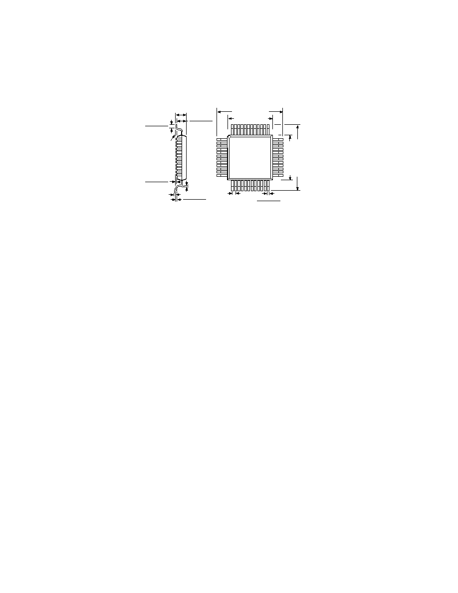
OUTLINE DIMENSIONS
Dimensions shown in inches and (mm).
48-Lead LQFP
(ST-48)
0.354 (9.00) BSC
0.276 (7.0) BSC
1
12
13
25
24
36
37
48
TOP VIEW
(PINS DOWN)
0.276 (7.0) BSC
0.354 (9.00) BSC
0.011 (0.27)
0.006 (0.17)
0.019 (0.5)
BSC
SEATING
PLANE
0.063 (1.60) MAX
0
°
MIN
0
°
7
°
0.006 (0.15)
0.002 (0.05)
0.030 (0.75)
0.018 (0.45)
0.057 (1.45)
0.053 (1.35)
0.030 (0.75)
0.018 (0.45)
0.007 (0.18)
0.004 (0.09)