AD5360/AD5361 16-Channel, 16/14-Bit, Serial Input, Voltage-Output DAC Preliminary Data Sheet (Rev. PrC)
16-Channel, 16/14-Bit,
Serial Input, Voltage-Output DAC
Preliminary Technical Data
AD5360/AD5361
Rev. Pr C
Information furnished by Analog Devices is believed to be accurate and reliable.
However, no responsibility is assumed by Analog Devices for its use, nor for any
infringements of patents or other rights of third parties that may result from its use.
Specifications subject to change without notice. No license is granted by implication
or otherwise under any patent or patent rights of Analog Devices. Trademarks and
registered trademarks are the property of their respective companies.
One Technology Way, P.O. Box 9106, Norwood, MA 02062-9106, U.S.A.
Tel: 781.329.4700
www.analog.com
Fax: 781.326.8703
© 2005 Analog Devices, Inc. All rights reserved.
FEATURES
16-channel DAC in 52-LQFP and 56-LFCSP
Guaranteed monotonic to 16/14 bits
Nominal output voltage range of -10 V to +10 V
Multiple output spans available
Temperature Monitoring Function
Channel Monitoring Multiplexer
GPIO Function
System calibration function allowing user-programmable
offset and gain
Channel grouping and addressing features
Data error checking feature
SPI compatible serial interface
2.5 V to 5.5 V JEDEC-compliant digital levels
Power-on reset
Digital reset (RESET)
Clear function to user-defined SIGGND (CLR pin)
Simultaneous update of DAC outputs (LDAC pin)
APPLICATIONS
Instrumentation
Industrial control systems
Level setting in automatic test equipment (ATE)
Variable optical attenuators (VOA)
Optical Line Cards
FUNCTIONAL BLOCK DIAGRAM
5360-0001
CONTROL
REGISTER
STATE
MACHINE
n
POWER-ON
RESET
SYNC
SDI
SCLK
SDO
BUSY
RESET
CLR
AD5360/
AD5361
SERIAL
INTERFACE
8
BIN/2SCOMP
VOUT8
VOUT9
VOUT10
VOUT11
VOUT12
VOUT13
VOUT14
VOUT15
SIGGND1
n
n
n
DAC 0
REGISTER
n
n
8
8
n
n
n
n
TO
MUX 2's
MUX
1
A/B SELECT
REGISTER
X1A REGISTER
X1B REGISTER
M REGISTER
C REGISTER
n
MUX
2
X2A REGISTER
X2B REGISTER
OFS1
REGISTER
14
14
DAC 0
OUTPUT BUFFER
AND POWER
DOWN CONTROL
OUTPUT BUFFER
AND POWER
DOWN CONTROL
OFFSET
DAC 1
BUFFER
n
n
n
DAC 7
REGISTER
n
n
n
n
n
n
MUX
1
X1A REGISTER
X1B REGISTER
M REGISTER
C REGISTER
n
MUX
2
X2A REGISTER
X2B REGISTER
DAC 7
·
·
·
·
·
·
·
·
·
·
·
·
·
·
·
·
·
·
·
·
·
·
·
·
·
·
·
·
·
·
·
·
·
·
·
·
·
·
·
·
·
·
·
·
·
·
·
·
·
·
·
·
·
·
GROUP 1
VREF0
SIGGND0
VOUT0
VOUT1
VOUT2
VOUT3
VOUT4
VOUT5
VOUT6
VOUT7
LDAC
DV
CC
V
DD
V
SS
AGND DNGD
n
n
n
DAC 0
REGISTER
n
n
8
8
n
n
n
n
TO
MUX 2's
MUX
1
A/B SELECT
REGISTER
X1A REGISTER
X1B REGISTER
M REGISTER
C REGISTER
n
MUX
2
X2A REGISTER
X2B REGISTER
OFS0
REGISTER
14
14
DAC 0
OUTPUT BUFFER
AND POWER
DOWN CONTROL
OUTPUT BUFFER
AND POWER
DOWN CONTROL
OFFSET
DAC 0
BUFFER
GROUP 0
·
·
·
·
·
·
·
·
·
·
·
·
·
·
·
·
·
·
·
·
·
·
·
·
·
·
·
·
·
·
·
·
·
·
·
·
·
·
·
·
·
·
·
·
·
·
·
·
·
·
·
·
·
·
n
n
n
DAC 7
REGISTER
n
n
n
n
n
n
MUX
1
X1A REGISTER
X1B REGISTER
M REGISTER
C REGISTER
n
MUX
2
X2A REGISTER
X2B REGISTER
DAC 7
BUFFER
VREF1
AD5360, n = 16
AD5361, n = 14
GPIO
REGISTER
TEMP
SENSOR
TEMP_OUT
PEC
MON_IN0
MON_IN1
GPIO
MON_OUT
VOUT0 -
VOUT15
MUX
6
2
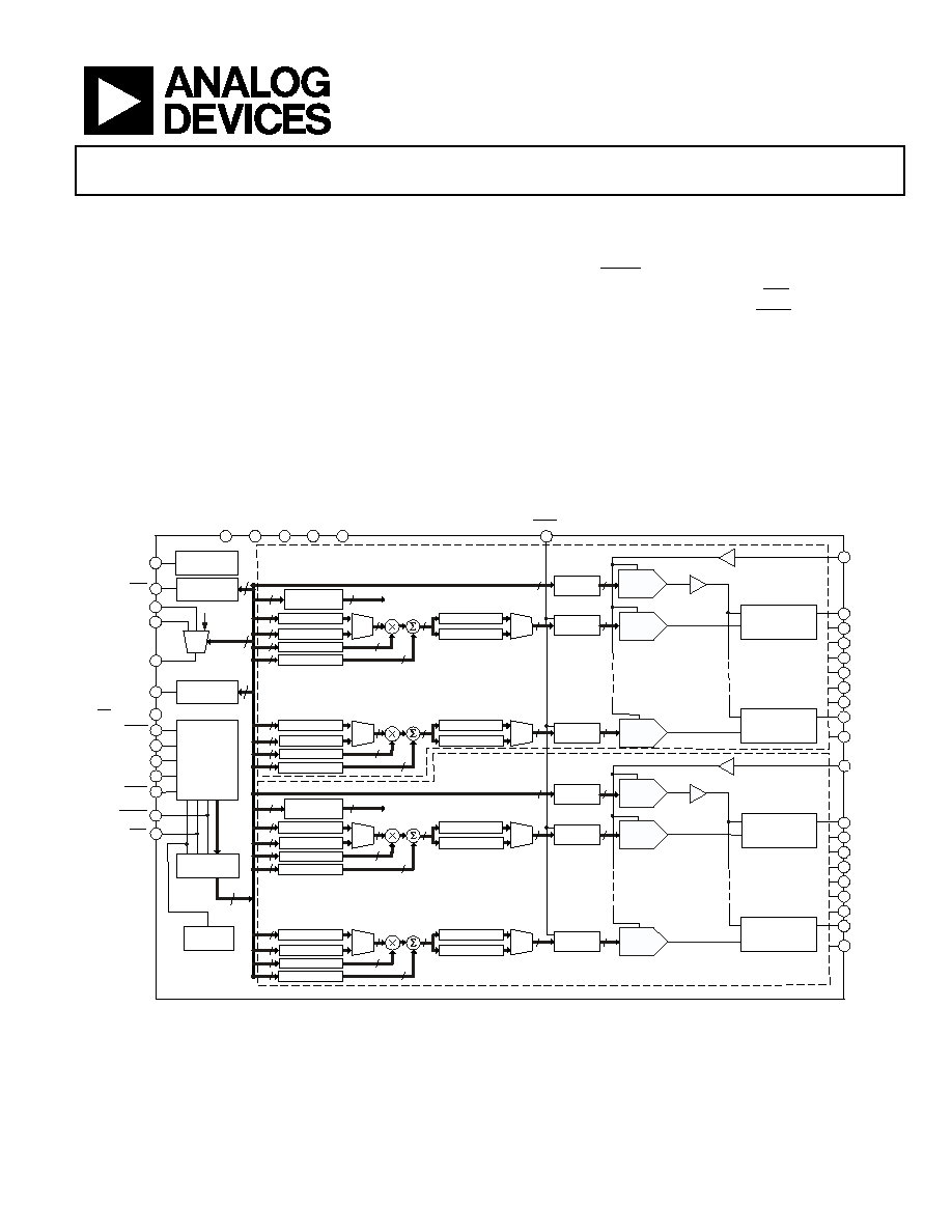
Figure 1.
AD5360/AD5361--Protected by U.S. Patent No. 5,969,657; other patents pending

AD5360/AD5361
Preliminary Technical Data
Rev. Pr C | Page 2 of 24
TABLE OF CONTENTS
General Description ......................................................................... 3
Specifications..................................................................................... 4
AC Characteristics........................................................................ 5
Timing Characteristics ................................................................ 6
Absolute Maximum Ratings............................................................ 8
ESD Caution.................................................................................. 8
Pin Configuration and Function Descriptions............................. 9
Terminology .................................................................................... 11
Functional Description .................................................................. 12
DAC Architecture--General..................................................... 12
Channel Groups.......................................................................... 12
A/ B Registers Gain/Offset Adjustment .................................. 13
Offset DACS................................................................................ 13
Output Amplifier........................................................................ 13
Transfer Function ....................................................................... 14
Reference Selection .................................................................... 14
Calibration................................................................................... 15
Reset Function ............................................................................ 15
Clear Function ............................................................................ 15
BUSY
And
LDAC
Functions..................................................... 15
Monitor Function....................................................................... 16
GPIO Pin ..................................................................................... 16
Power-Down Mode .................................................................... 16
Thermal Monitoring Function ................................................. 16
Toggle Mode................................................................................ 16
Serial Interface ................................................................................ 18
SPI Write Mode .......................................................................... 18
Register Update Rates ................................................................ 18
SPI Readback Mode ................................................................... 19
Channel Addressing And Special Modes................................ 19
Special Function Mode.............................................................. 20
Power Supply Decoupling ......................................................... 22
Power Supply Sequencing ......................................................... 22
Interfacing Examples ................................................................. 23
Outline Dimensions ....................................................................... 24
Ordering Guide .......................................................................... 24
REVISION HISTORY
Pr B2. Modified SPI Timing Diagrams
Added Reference Selection and Calibration text

Preliminary Technical Data
AD5360/AD5361
Rev. Pr C | Page 3 of 24
GENERAL DESCRIPTION
The AD5360/AD5361 contains 16, 16/14-bit DACs in a single,
56-lead, LFCSP or 52-lead LQFP package. It provides buffered
voltage outputs with a span 4 times the reference voltage. The
gain and offset of each DAC can be independently trimmed to
remove errors. For even greater flexibility, the device is divided
into two blocks of 8 DACs, and the output range of each block
can be independently adjusted by an offset DAC.
The AD5360/AD5361 offers guaranteed operation over a wide
supply range with V
SS
from -4.5 V to -16.5 V and V
DD
from
+8 V to +16.5 V. The output amplifier headroom requirement is
1.4 V operating with a load current of 1 mA.
The AD5360/AD5361 has a high-speed 4-wire serial interface,
which is compatible with SPI®, QSPITM, MICROWIRETM, and DSP
interface standards and can handle clock speeds of up to 50
MHz. All the outputs can be updated simultaneously by taking
the LDAC input low. Each channel has a programmable gain
and an offset adjust register.
Each DAC output is amplified and buffered on-chip with
respect to an external SIGGND input. The DAC outputs can
also be switched to SIGGND via the CLR pin.
Table 1. High Channel Count Bipolar DACs
Model Resolution
Nominal
Output
Span
Output
Channels
Linearity Error
(LSB)
Package Description
Package Option
AD5360BCPZ
16 Bits
4
×
V
REF
(20 V)
16
±4
56-Lead LFCSP
CP-56
AD5360BSTZ
16 Bits
4
×
V
REF
(20 V)
16
±4
52-Lead LQFP
ST-52
AD5361BCPZ
14 Bits
4
×
V
REF
(20 V)
16
±1
56-Lead LFCSP
CP-56
AD5361BSTZ
14 Bits
4
×
V
REF
(20 V)
16
±1
52-Lead LQFP
ST-52
AD5362BCPZ 16
Bits
4
×
V
REF
(20 V)
8
±4
56-Lead LFCSP
CP-56
AD5362BSTZ 16
Bits
4
×
V
REF
(20 V)
8
±4
52-Lead LQFP
ST-52
AD5363BCPZ
14 Bits
4
×
V
REF
(20 V)
8
±1
56-Lead LFCSP
CP-56
AD5363BSTZ
14 Bits
4
×
V
REF
(20 V)
8
±1
52-Lead LQFP
ST-52
AD5370BCPZ
16 Bits
4
×
V
REF
(12 V)
40
±4
64-Lead LFCSP
CP-64
AD5370BSTZ
16 Bits
4
×
V
REF
(12 V)
40
±4
64-Lead LQFP
ST-64
AD5371BCPZ
14 Bits
4
×
V
REF
(12 V)
40
±1
100-Ball CSPBGA
BC-100-2
AD5371BSTZ
14 Bits
4
×
V
REF
(12 V)
40
±1
80-Lead LQFP
ST-80
AD5372BCPZ
16 Bits
4
×
V
REF
(12 V)
32
±4
56-Lead LFCSP
CP-56
AD5372BSTZ
16 Bits
4
×
V
REF
(12 V)
32
±4
64-Lead LQFP
ST-64
AD5373BCPZ
14 Bits
4
×
V
REF
(12 V)
32
±1
56-Lead LFCSP
CP-56
AD5373BSTZ
14 Bits
4
×
V
REF
(12 V)
32
±1
64-Lead LQFP
ST-64

AD5360/AD5361
Preliminary Technical Data
Rev. Pr C | Page 4 of 24
SPECIFICATIONS
DV
CC
= 2.3 V to 5.5 V; V
DD
= 11.4 V to 16.5 V; V
SS
= -11.4 V to -16.5 V; V
REF
= 5 V; AGND = DGND = SIGGND = 0 V; R
L
= Open
Circuit; Gain (m), Offset(c) and DAC Offset registers at default value; all specifications T
MIN
to T
MAX
, unless otherwise noted.;
Table 2. Performance Specifications
Parameter B
Version
1
Unit
Test
Conditions/Comments
1
ACCURACY
Resolution 16
Bits
AD5360
14
Bits
AD5361
Relative Accuracy
±4
LSB max
AD5360
±1
LSB
max
AD5361
Differential Nonlinearity
±1
LSB max
Guaranteed monotonic by design over temperature.
Offset Error
±20
mV max
Prior to calibration
Gain Error
±20
mV max
Prior to calibration
Offset Error
2
100
µV max
After calibration
Gain Error
2
100
µV max
After calibration
VOUT Temperature Coefficient
5
ppm FSR/°C typ
Includes linearity, offset, and gain drift.
DC Crosstalk
1
0.5
mV max
Typically 100 µV.
REFERENCE INPUTS (VREF1, VREF2)
1
V
REF
DC Input Impedance
1
M min
Typically 100 M.
V
REF
Input Current
±10
µA max
Per input. Typically ±30 nA.
V
REF
Range
4
2/5
V min/max
±2% for specified operation.
SIGGND INPUT (SIGGND0, TO SIGGND1)
1
DC Input Impedance
55
k min
Typically 60 k.
Input Range
±0.5
V min/max
OUTPUT CHARACTERISTICS
1
Output Voltage Range
V
SS
+ 1.4
V min
I
LOAD
= 1 mA.
V
DD
- 1.4
V max
I
LOAD
= 1 mA.
Nominal Output Voltage Range
-10 to +10
V
Short Circuit Current
10
mA max
Load Current
±1
mA max
Capacitive Load
2200
pF max
DC Output Impedance
0.5
max
MONITOR PIN (MON_OUT)
Output Impedance
500
typ
Three State Leakage Current
100
nA typ
Continuous Current Limit
2
mA max
DIGITAL INPUTS
JEDEC compliant.
Input High Voltage
1.7
V min
DV
CC
= 2.3 V to 3.6 V.
2.0
V
min
DV
CC
= 3.6 V to 5.5 V.
Input Low Voltage
0.8
V max
DV
CC
= 2.5 V to 5.5 V.
0.7
V
DV
CC
= 2.3 V to 2.7 V.
Input Current
±1
µA max
All other digital input pins.
Input Capacitance
1
10
pF
max
DIGITAL OUTPUTS (SDO, BUSY, GPIO, PEC)
Output Low Voltage
0.5
V max
Sinking 200 µA.
Output High Voltage (SDO)
DV
CC
- 0.5
V min
Sourcing 200 µA.
High Impedance Leakage Current
±5
µA max
SDO only.
High Impedance Output Capacitance
10
pF typ

Preliminary Technical Data
AD5360/AD5361
Rev. Pr C | Page 5 of 24
Parameter B
Version
1
Unit
Test
Conditions/Comments
1
TEMPERATURE SENSOR (TMP_OUT)
Accuracy
±1
°C
@25 °C
±5
°C max
-40 °C < T < +85°C
Output Voltage at 25 °C
1.5
V typ
Output Voltage Scale Factor
5
mV/°C typ
Output Voltage Range
0/3
V min/max
Output Load Current
200
µA max
Current source only.
Power On Time
10
ms typ
To within ±5 °C
POWER REQUIREMENTS
DV
CC
2.3/5.5
V
min/max
V
DD
8/16.5
V
min/max
V
SS
-4.5/-16.5
V
min/max
Power Supply Sensitivity
1
Full Scale/ V
DD
-75
dB
typ
Full Scale/ V
SS
-75
dB
typ
Full Scale/ V
CC
-90
dB
typ
DI
CC
2
mA
max
V
CC
= 5.5 V, V
IH
= V
CC
, V
IL
= GND.
I
DD
7
mA max
Outputs unloaded.
I
SS
7
mA max
Outputs unloaded.
Power Dissipation
Power Dissipation Unloaded (P)
173
mW
V
SS
= -12 V, V
DD
= +12 V, DV
CC
= 2.5 V
Junction Temperature
130
°C max
T
J
= T
A
+ P
TOTAL
×
J
3
1
Temperature range for B Version: -40°C to +85°C. Typical specifications are at 25°C.
2
Guaranteed by design and characterization, not production tested.
3
Where
J
represents the package thermal impedance.
4
. Specifications are guaranteed for a 5V reference only.
AC CHARACTERISTICS
DV
CC
= 2.5 V; V
DD
= 15 V; V
SS
= -15 V; V
REF
= 5 V; AGND = DGND = SIGGND = 0 V; R
L
= 10 k to GND; C
L
= 200 pF to GND;
Gain (m), Offset(c) and DAC Offset registers at default values; all specifications T
MIN
to T
MAX
, unless otherwise noted.
Table 3. AC Characteristics
Parameter
B Version
1,2
Unit Test
Conditions/Comments
DYNAMIC PERFORMANCE
Output Voltage Settling Time
TBD
µs typ
Full-scale change
30
µs max
DAC latch contents alternately loaded with all 0s and all 1s.
Slew Rate
1
V/µs typ
Digital-to-Analog Glitch Energy
20
nV-s typ
Glitch Impulse Peak Amplitude
10
mV max
Channel-to-Channel Isolation
100
dB typ
DAC-to-DAC Crosstalk
40
nV-s typ
Between DACs inside a group.
10
nV-s typ
Between DACs from different groups.
Digital Crosstalk
0.1
nV-s typ
Digital Feedthrough
1
nV-s typ
Effect of input bus activity on DAC output under test.
Output Noise Spectral Density @ 10 kHz
250 nV/(Hz)
1/2
typ
V
REF
= 0 V.
1
Temperature range for B Version: -40°C to +85°C. Typical specifications are at 25°C.
2
Guaranteed by design and characterization, not production tested.