þÿ

LPC TO ISA BRIDGE SET
W83626F/W83626D
PRELIMINARY
Publication Release Date: Feb 2000
- 1 - Revision 0.50
GENERAL DESCRIPTION
W83626F/W83626D is a transparent LPC-to-ISA bus conversion IC.
For the new generation Intel chipset Camino and Whitney, SiS Super South 960,
featuring LPC bus, there is no support for ISA bus and slots. However the demand of
ISA devices still exist. For such case, W83626F is the best companion solution for the
non-ISA chipset. Also the packages of W83626F had been chosen to be the most
economic solution for save the M/B board layout size and cost.
For the new generation chipset featuring LPC interface and support no ISA bus,
W83627HF (Winbond LPC I/O) together with the set of W83626F is the complete
solution.
FEATURES
LPC to ISA Bridge
· Meet LPC Spec. 1.1
· Support LDRQ# (LPC DMA), SERIRQ (serial IRQ)
·
Full ISA Bus Support except ISA Bus Masters, 16 bit I/O and Memory R/W
·
5V ISA and 3.3V LPC interfaces
· All
Software Transparent
·
IRQ Serializer for ISA Parallel IRQ transfer to Serial IRQ
·
Supports 3 fully ISA Compatible Slots without Buffering
· LPC
Bus at 33MHz
·
Supports Programmable ISA Bus Divide the PCI Clock into 3 or 4
·
All ISA Signals can be Isolate
· 14.318MHz in to generate two 14.318MHz buffer out and one 24.576MHz
· Specific Keyboard Functions supported
· Support 8 programmable general purpose I/O pins
·
Supports Configuration registers for programming performance
PACKAGE
· 128-pin PQFP for W83626F
LPC TO ISA BRIDGE SET
W83626F/W83626D
PRELIMINARY
Publication Release Date: Feb 2000
- 2 - Revision 0.50
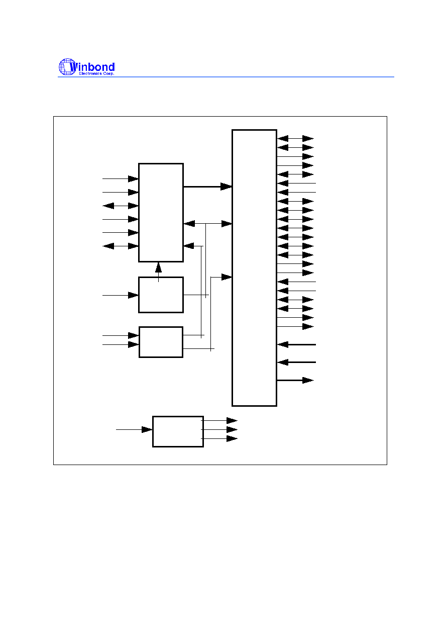
Block diagram OF W83626F
LFRAM#
LPC
Interface
BALE
AEN
ISA
Interface
SA[19:0]
SD[15:0]
IOCHRDY
IOCS16#
IOCHK#
IOR#
IOW#
LA[23:17]
SBHE#
MEMCS16#
MEMR#
MEMW#
SMEMR#
SMEMW#
ZEROWS#
MASTER#
REFRESH#
RSTDRV
SYSCLK
ISOLATE#
Signal
Isolation
Control
Power
SuppIy
3.3V
5V
ROMCS#
PCIRST#
PCICLK
LDRQ#
LAD[3:0]
SERIRQ
CLOCK
GEN. / BUF.
14.318M
14MOUT1
14MOUT2
24.576M
IRQ[3:7,9:12,14,15]
DRQ[0:3,5:7]
DACK[0:3,5:7]
LPC TO ISA BRIDGE SET
W83626F/W83626D
PRELIMINARY
Publication Release Date: Feb 2000
- 3 - Revision 0.50
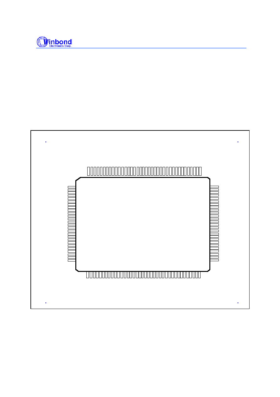
PIN CONFIGURATION FOR 626F
GP
I
O
6
/
R
T
CC
S#
64
63
62
61
60
59
58
57
56
55
54
53
52
51
50
49
48
47
46
45
44
43
42
41
40
39
103
104
105
106
107
108
109
110
111
112
113
114
115
116
117
118
119
120
121
122
123
124
125
126
127
128
2 1 0
1
0
1
0
1
0
9
9
9
8
9
7
9
6
9
5
9
4
9
3
9
2
9
1
9
0
8
9
8
8
8
7
8
6
8
5
8
4
8
3
8
2
8
1
8
0
7
9
7
8
7
7
7
6
7
5
7
4
7
3
7
2
7
1
7
0
6
9
6
8
6
7
6
6
6
5
1 2 3 4 5 6 7 8 9
1
0
1
1
1
2
1
3
1
4
1
5
1
6
1
7
1
8
1
9
2
0
2
1
2
2
2
3
2
4
2
5
2
6
2
7
2
8
2
9
3
0
3
1
3
2
3
3
3
4
3
5
3
6
3
7
3
8
DR
Q5
DA
CK
5#
DR
Q0
DA
CK
0#
VC
C5
IR
Q1
4
IR
Q1
5
IR
Q1
1
IR
Q1
2
IR
Q1
0
IO
CS
1
6
#
ME
MC
S
1
6
#
LFRAM
#
PC
I
R
ST# GN
D
LAD
3
LAD
2
LAD
1
LAD
0
VC
C3
PC
I
C
LK
LD
R
Q
#
SE
RI
RQ
P
W
RD
N#
14.31
8M
14M
O
U
T1
14M
O
U
T2
24.57
6M
SA
0
AV
CC
3
SA
1
SA
2
SA
3
SA
4
G
P
IO
0
/
IR
Q1
RO
M
C
S#
AG
ND
80PC
S
#
/
KB
E
N
#
GPIO5/IRQ8
GPIO4/PLED
GPIO3/IRQIN
IOCHRDY
GND
AEN
SA19
SA18
SA17
VCC5
SA16
SA15
SA14
SA13
GND
SA12
SA11
SA10
SA9
VCC5
SA8
SA7
SA6
SA5
GPIO2/MCCS#
GPIO1/KBCS#
G
P
IO
7
/
IO
H
C
S
#
SD
0
SD
1
SD
2
VC
C5
SD
3
SD
5
SD
4
SD
6
OW
S#
SD
7
I
O
C
HCK
#
RS
T
D
R
V
IR
Q9
DR
Q2
GN
D
SM
EM
W
#
SM
EM
R#
VC
C5
IO
W#
IO
R#
DA
CK
3#
DR
Q3
TC DA
CK
2#
BA
LE
IR
Q3
IR
Q4
IR
Q5
GN
D
IR
Q6
RE
F
R
E
S
H
#
SY
SC
L
K
IR
Q7
DR
Q1
DA
CK
1#
SB
HE
#
LA23
LA22
VCC5
LA21
LA20
LA19
LA18
GND
LA17
MEMR#
MEMW#
SD8
SD10
SD9
SD11
SD12
SD13
VCC5
SD14
SD15
MASTER#/RTCEN
DRQ7
GND
DACK7#
DRQ6
DACK6#/HEFRAS
W83626F
LPC to ISA
LPC TO ISA BRIDGE SET
W83626F/W83626D
PRELIMINARY
Publication Release Date: Feb 2000
- 4 - Revision 0.50
1. PIN DESCRIPTION
I/O12t
- TTL level bi-directional pin with 12 m A source-sink capability
I/O24t
- TTL level bi-directional pin with 24 m A source-sink capability
I/O12tp3
- 3.3V TTL level bi-directional pin with 12 m A source-sink capability
I/O24tp3
- 3.3V TTL level bi-directional pin with 24 m A source-sink capability
I/OD12t
- TTL level bi-directional pin open drain output with 12 m A sink capability
I/O24t
- TTL level bi-directional pin with 24 m A source-sink capability
OUT12
- TTL level output pin with 12 m A source-sink capability
OUT24
- TTL level output pin with 24 m A source-sink capability
O12p3
- 3.3V TTL level output pin with 12 m A source-sink capability
O24p3
- 3.3V TTL level output pin with 24 m A source-sink capability
OD12
- Open-drain output pin with 12 m A sink capability
OD24
- Open-drain output pin with 24 m A sink capability
INcs
- CMOS level Schmitt-trigger input pin
INt
- TTL level input pin
INtd
- TTL level input pin with internal pull down resistor
INtu
- TTL level input pin with internal pull up resistor
INts
- TTL level Schmitt-trigger input pin
INtsp3
- 3.3V TTL level Schmitt-trigger input pin
W83626F PIN DESCRIPTION
LPC Interface
SYMBOL PIN I/O
FUNCTION
LAD[3:0]
16-19
I/O
12tp3
These signal lines communicate address, control and data
information over the LPC bus between a host and a peripheral.
LFRAME#
13
IN
tsp3
Indicates start of a new cycle or termination of a broken cycle.
PCICLK
21
INt
PCICLK provides timing for all transactions on the LPC bus. All
LPC signals are sampled on the rising edge of PCICLK, and all
timing parameters are defined with respect to this edge.
PCIRST#
14
INtsp3 Reset signal. It can connect to PCIRST# signal on the host.
SERIRQ
23
I/OD12t Serial IRQ Input/Output.
LDRQ#
22
O
12tp3
Encoded DMA Request signal.
LPC TO ISA BRIDGE SET
W83626F/W83626D
PRELIMINARY
Publication Release Date: Feb 2000
- 5 - Revision 0.50
LPC Interface, continued
SYMBOL PIN I/O
FUNCTION
PWRDN#
24
INtu
Power Down. The signal is active low according to CR 44 Bit 7and
wake-up enable by hardware setting. There are eight different
power-down states (Power down Mode 3).
ISA Interface Signals
SYMBOL PIN I/O
FUNCTION
SA[19:17]
58-56
OUT24 System Address Bus. These are the upper address lines that
define the ISA's byte granular address space (up to 1 M byte).
SA[19:17] are at an unknown state upon PCIRST#.
SA[16:0]
54-51
49-46
44-41
35-31
OUT24 System Address Bus. These are the bi-directional lower address
lines that define the ISA's byte granular address space (up to 1 M
byte). SA[16:0] are at an unknown state upon PCIRST#.
SD[15:0]
122-1
21
119-1
14
75-71
69-67
OUT24 System Data. SD[15:0] provide the 16-bit data path for devices
residing on the ISA Bus. The W83626F tri-states SD[15:0] during
PCIRST#.
AEN
59
OUT24 Address Enable. AEN is asserted during DMA cycles. This signal
is also driven high during W83626F initiated refresh cycles. AEN is
driven low upon PCIRST#.
IOR#
86
OUT24 I/O Read. IOR# is the command to an ISA I/O slave device that the
slave may drive data on to the ISA data bus (SD[15:0]).
IOW#
84
OUT24 I/O Write. IOW# is the command to an ISA I/O slave device that
the slave may latch data from the ISA data bus (SD[15:0]).
IOCHRDY
61
INt
I/O Channel Ready. Resources on the ISA Bus negate IOCHRDY
to indicate that additional time (wait states) is required to complete
the cycle.
SYSCLK
92
OUT24 ISA System Clock. SYSCLK is the reference clock for the ISA
bus. The SYSCLK is generated by dividing PCICLK by 3 or 4.
RSTDRV
77
OUT24
Reset Drive. W83628F asserts RSTDRV to reset devices that
reside on the ISA Bus. The W83628F asserts this signal while the
PCIRST# is asserted.
IOCS16#
11
INt
16-bit I/O Chip Select. This signal is driven by I/O devices on the
ISA Bus to indicate that they support 16-bit I/O bus cycles.
Document Outline