NLT06-80-PA ds02-267 2-23-03final.fm
NetLight
®
NLT06-80-PA 622 Mb/s 1550 nm Laser Transceiver
for Extended Long Reach
Preliminary Data Sheet
February 2003
TriQuint Optoelectronics
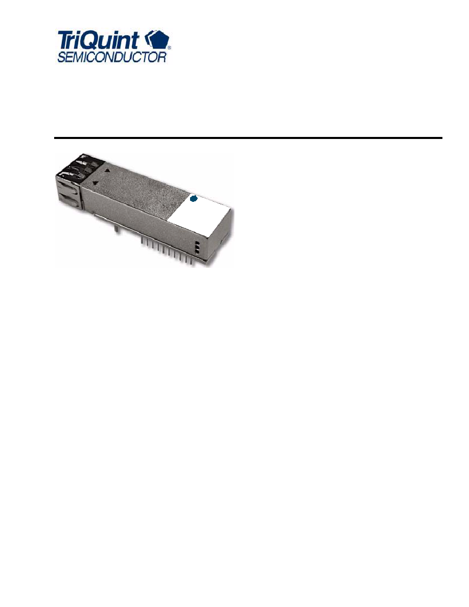
Available in a small form-factor, metal package with LC recepta-
cle connector, the NLT06-80-PA transceiver is a high-perfor-
mance, cost-effective, optical transceiver for SONET/SDH
applications.
Features
Small form-factor, 20-pin package
LC duplex receptacle
Uncooled 1550 nm DFB laser transmitter with auto-
matic output power control
Transmitter disable input
Wide dynamic range receiver with InGaAs PIN pho-
todetector
Laser bias and back-facet PIN monitors
LVTTL signal-detect output
Low power dissipation
Single 3.3 V power supply
LVPECL compatible data inputs and outputs
Operating temperature range of 40
°C to +85 °C
Telecom reliability (GR-468-CORE RT)
Wave solderable and aqueous wash compatible
Applications
SONET LR-2 OC-12, ITU L-4.2 80 km applications
Description
The NLT06-80-PA transceiver is a high-speed, cost-
effective optical transceiver that is intended for
622 Mb/s SONET LR-2 OC-12 and ITU L-4.2
80 km applications. The transceiver features TriQuint
optics and is packaged in a narrow-width metal hous-
ing with an LC duplex receptacle. The 20-pin package
pinout conforms to a multisource transceiver agree-
ment.
The transmitter features the ability to interface to
LVPECL differential logic level data inputs. The trans-
mitter also features a LVTTL logic level disable input
and laser bias and back-facet monitor outputs. The
receiver features differential LVPECL logic level data
outputs, a LVTTL logic level signal-detect output and
direct access to the PIN photodetector bias input for
photocurrent monitoring purposes.
®
riQ
T
uin
t
SE
M
IC
ON
DU
CT
OR
NL
T
Tra
ns
ce
ive
r
®
riQ
T
ui
nt
SE
M
IC
O
ND
UC
TO
R
Tr
an
sc
ei
ve
r
NL
T
2
For additional information and latest specifications, see our website: www.triquint.com
NetLight NLT06-80-PA 622 Mb/s 1550 nm Laser Transceiver
Preliminary Data Sheet
for Extended Long Reach
February 2003
Absolute Maximum Ratings
Stresses in excess of the absolute maximum ratings can cause permanent damage to the device. These are abso-
lute stress ratings only. Functional operation of the device is not implied at these or any other conditions in excess
of those given in the operations sections of the data sheet. Exposure to absolute maximum ratings for extended
periods can adversely affect device reliability.
Table 1. Absolute Maximum Ratings
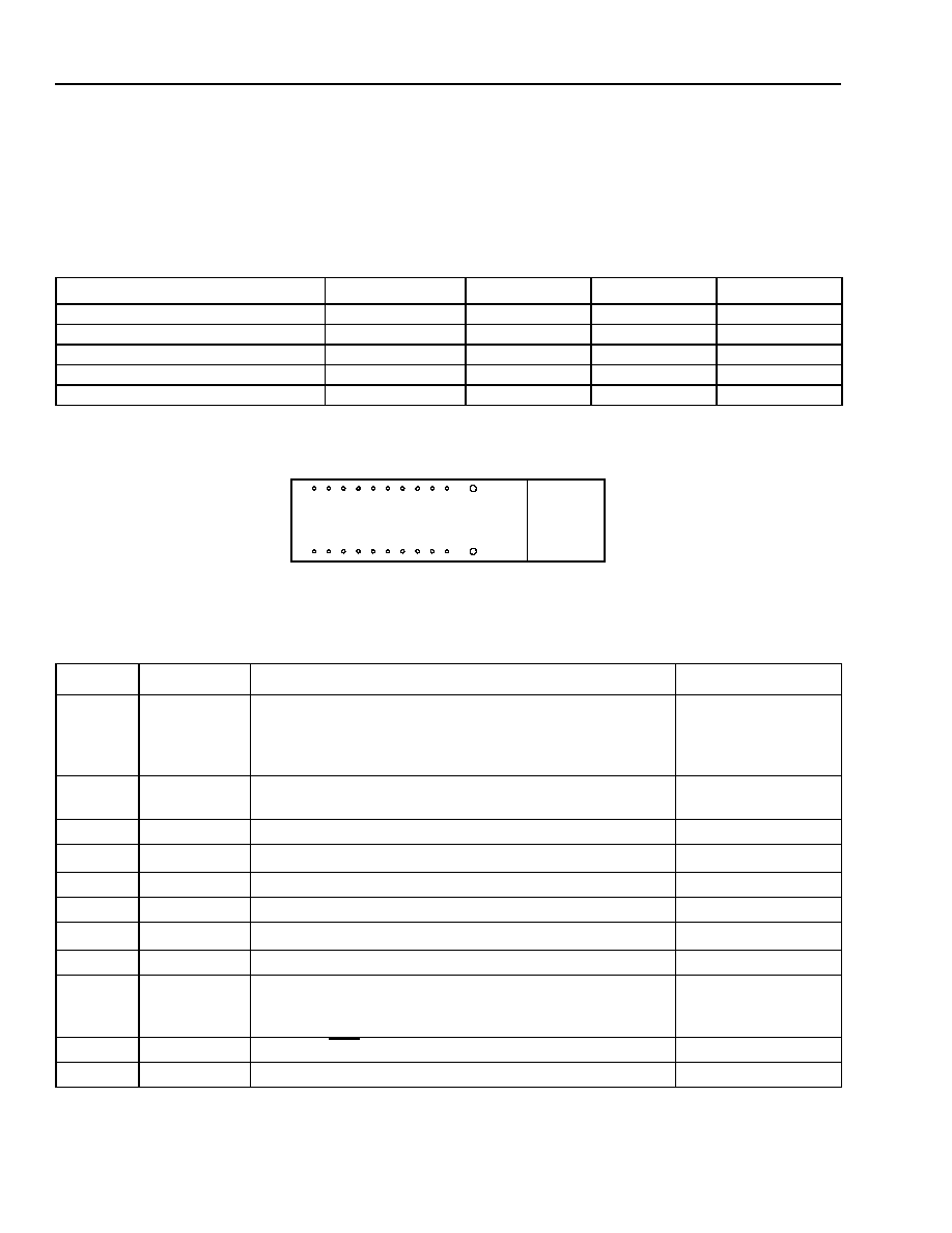
Pin Information
Figure 1. Top View of the NLT06-80-PA Transceiver, 20-Pin Configuration
Parameter
Symbol
Min
Max
Unit
Supply Voltage
V
CC
0
5
V
Operating Case Temperature Range
T
C
40
85
°C
Storage Temperature Range
T
S
40
85
°C
Lead Soldering Temperature/Time
--
--
260/10
°C/s
Operating Wavelength Range
1.2
1.6
µm
Table 2. Receiver Pin Descriptions
Pin #
Symbol
Functional Description
Logic Family
MS
MS
Mounting Studs. The mounting studs are provided for
transceiver mechanical attachment to the circuit board. They
can also provide an optional connection of the transceiver to
the equipment chassis ground.
NA
1
V
PD
Photodetector Bias Input. This lead supplies bias for the
PIN photodetector diode.
NA
2
V
EER
Receiver Signal Ground.
NA
3
V
EER
Receiver Signal Ground.
NA
4
NIC
No Internal Connection.
NA
5
NIC
No Internal Connection.
NA
6
V
EER
Receiver Signal Ground.
NA
7
V
CCR
Receiver Power Supply.
NA
8
SD
Signal Detect.
Normal operation: logic one output.
Fault condition: logic zero output.
LVTTL
9
RD
Received
Data
Out.
LVPECL
10
RD+
Received Data Out.
LVPECL
6
7
8
9
10
15
14
13
12
11
T
X
R
X
1
2
3
4
5
20
19
18
17
16

For additional information and latest specifications, see our website: www.triquint.com
3
Preliminary Data Sheet
NetLight NLT06-80-PA 622 Mb/s 1550 nm Laser Transceiver
February 2003
for Extended Long Reach
Pin Information
(continued)
Table 3. Transmitter Pin Descriptions
Pin #
Symbol
Functional Description
Logic Family
11
V
CCT
Transmitter Power Supply.
NA
12
V
EET
Transmitter Signal Ground.
NA
13
TD
IS
Transmitter Disable.
LVTTL
14
TD+
Transmitter Data In.
LVPECL
15
TD
Transmitter
Data
In.
LVPECL
16
V
EET
Transmitter Signal Ground.
NA
17
B
MON
()
Laser Diode Bias Current Monitor--Negative End.
Optional feature. If feature is not used, do not connect.
The laser bias current is accessible as a dc voltage by mea-
suring the voltage developed across pins 17 and 18.
NA
18
B
MON
(+)
Laser Diode Bias Current Monitor--Positive End.
Optional feature. If feature is not used, do not connect.
See pin 17 description.
NA
19
P
MON
()
Laser Diode Optical Power Monitor--Negative End.
Optional feature. If feature is not used, do not connect. The
back-facet diode monitor current is accessible as a voltage
proportional to the photocurrent through a 200
resistor
between pins 19 and 20.
NA
20
P
MON(
+)
Laser Diode Optical Power Monitor--Positive End.
Optional feature. If feature is not used, do not connect.
See pin 19 description.
NA
Electrostatic Discharge
Caution: This device is susceptible to damage as a
result of electrostatic discharge (ESD).
Take proper precautions during both han-
dling and testing. Follow EIA
®
Standard
EIA-625.
Although protection circuitry is designed into the
device, take proper precautions to avoid exposure to
ESD.
TriQuint employs a human-body model (HBM) for ESD
susceptibility testing and protection-design evaluation.
ESD voltage thresholds are dependent on the critical
parameters used to define the model. A standard HBM
(resistance = 1.5 k
, capacitance = 100 pF) is widely
used and, therefore, can be used for comparison pur-
poses. The HBM ESD threshold established for the
NLT06-80-PA is ±1000 V.
Application Information
The NLT receiver section is a highly sensitive fiber-
optic receiver. Although the data outputs are digital
logic levels, the device should be thought of as an ana-
log component. When laying out system application
boards, the NLT transceiver should receive the same
type of consideration given to a sensitive analog com-
ponent.
Printed-Wiring Board Layout Considerations
A fiber-optic receiver employs a very high gain, wide-
bandwidth transimpedance amplifier. This amplifier
detects and amplifies signals that are only tens of nA in
amplitude when the receiver is operating near its sensi-
tivity limit. Any unwanted signal currents that couple
into the receiver circuitry cause a decrease in the
receiver's sensitivity and can also degrade the perfor-
mance of the receiver's signal-detect (SD) circuit.

NetLight NLT06-80-PA 622 Mb/s 1550 nm Laser Transceiver
Preliminary Data Sheet
for Extended Long Reach
February 2003
4
4
For additional information and latest specifications, see our website: www.triquint.com
Application Information
(continued)
Printed-Wiring Board Layout Considerations
(continued)
To minimize the coupling of unwanted noise into the
receiver, careful attention must be given to the printed-
wiring board.
At a minimum, a double-sided printed-wiring board
(PWB) with a large component-side ground plane
beneath the transceiver must be used. In applications
that include many other high-speed devices, a multi-
layer PWB is highly recommended. This permits the
placement of power and ground on separate layers,
which allows them to be isolated from the signal lines.
Multilayer construction also permits the routing of sen-
sitive signal traces away from high-level, high-speed
signal lines. To minimize the possibility of coupling
noise into the receiver section, high-level, high-speed
signals such as transmitter inputs and clock lines
should be routed as far away as possible from the
receiver pins.
Noise that couples into the receiver through the power
supply pins can also degrade performance. It is recom-
mended that the pi filter, shown in Figure 2, be used for
both the transmitter and receiver power supplies.
Data and Signal-Detect Outputs
Due to the high switching speeds of LVPECL outputs,
transmission line design must be used to interconnect
components. To ensure optimum signal fidelity, both
data and clock outputs should be terminated identically.
The signal lines connecting the data outputs to the next
device should be equal in length and have matched
impedances. Controlled-impedance stripline or micros-
trip construction must be used to preserve the quality
of the signal into the next component and to minimize
reflections back into the receiver, which could degrade
its performance. Excessive ringing due to reflections
caused by improperly terminated signal lines makes it
difficult for the component receiving these signals to
decipher the proper logic levels and can cause transi-
tions to occur where none were intended. Also, by min-
imizing high-frequency ringing, possible EMI problems
can be avoided.
The signal-detect output is positive LVTTL logic. A logic
low at this output indicates that the optical signal into
the receiver has been interrupted or that the light level
has fallen below the minimum signal-detect threshold.
This output should not be used as an error rate indica-
tor since its switching threshold is determined only by
the magnitude of the incoming optical signal.
Transceiver Processing
When the process plug is placed in the transceiver's
optical port, the transceiver and plug can withstand
normal wave soldering and aqueous spray cleaning
processes. However, the transceiver is not hermetic,
and should not be subjected to immersion in cleaning
solvents. The transceiver case should not be exposed
to temperatures in excess of 125 °C. The transceiver
pins can be wave soldered at 260 °C for up to 10 sec-
onds. The process plug should only be used once.
After removing the process plug from the transceiver, it
must not be used again as a process plug; however, if
it has not been contaminated, it can be reused as a
dust cover.

For additional information and latest specifications, see our website: www.triquint.com
5
Preliminary Data Sheet
NetLight NLT06-80-PA 622 Mb/s 1550 nm Laser Transceiver
February 2003
for Extended Long Reach
Transceiver Optical and Electrical Characteristics
1. TTL compatible interface.
1. 2
23
1 PRBS with a BER of 1 x 10
10
.
Table 4. Transmitter Optical and Electrical Characteristics (T
C
= 40
°C to +85 °C, V
CC
= 3.135 V--3.465 V.
All parameters must meet the specifications over the entire lifetime.)
Parameter
Symbol
Min
Max
Unit
Average Optical Output Power (EOL)
P
O
3
2
dBm
Optical Wavelength
c
1480
1580
nm
Side-mode Suppression Ratio
SMSR
30
--
dB
Dynamic Extinction Ratio
EXT
10
--
dB
Output Optical Eye
Compliant with SONET GR-253-CORE and
ITU-T G.957 Eye Mask Requirements
Power Supply Current
I
CCT
--
150
mA
Input Data Voltage:
High
Low
V
IH
V
IL
V
CC
1.165
V
CC
1.810
V
CC
0.880
V
CC
1.475
V
V
Transmit Disable Voltage
1
V
D
Vcc 0.9
Vcc
V
Transmit Enable Voltage
1
V
EN
V
EE
V
EE
+ 0.8
V
Transmit Enable Time
T
EN
--
1
ms
Transmit Disable Time
T
DIS
--
10
µs
Laser Bias Voltage
V
BIAS
0.0
0.7
V
Laser Back-facet Monitor Voltage
V
BF
0.01
0.2
V
Table 5. Receiver Optical and Electrical Characteristics (T
C
= 40
°C to +85 °C, V
CC
= 3.135 V--3.465 V)
Parameter
Symbol
Min
Max
Unit
Average Sensitivity
1
P
I
--
28
dBm
Maximum Input Power
1
P
MAX
8
--
dBm
Power Supply Current
I
CCR
--
150
mA
Output Data Voltage:
High
Low
V
OH
V
OL
V
CC
1.025
V
CC
1.810
V
CC
0.880
V
CC
1.620
V
V
Signal-detect Switching Threshold
Assert
Deassert
LSTD
LSTI
45
--
29.0
28.5
dBm
dBm
Signal-detect Hysteresis
HYS
0.5
6
dB
Signal-detect Voltage
Low
High
V
OL
V
OH
0.0
2.4
0.8
V
CC
V
V
Signal-detect Response Time
SDRT
--
100
µs
Document Outline