Äîêóìåíòàöèÿ è îïèñàíèÿ www.docs.chipfind.ru
www.ti.com
FEATURES
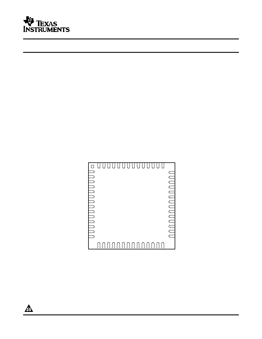
TBD PACKAGE
(TOP VIEW)
1
2
3
4
5
6
7
8
9
10
11
12
13
14
RFPD
PAPDA
PAPDB
ABSEL
V+RFLO
GND
LON
LOP
GND
V+CP
RSVD2
RFLOBP
RFLOTUN
RFLOCP
15
16
17
18
19
20
21
22
23
24
25
26
27
28
RSVD3
XT
ALO
V+D
CLKON
XT
ALBYP
CLKOP
V+CLK
CLK
DA
T
A
EN
CALEN
XT
ALI
GND
REFDIV
42
41
40
39
38
37
36
35
34
33
32
31
30
29
GND
RXQP
RXQN
RXIP
RXIN
GND
V+IFLO
STATUS
PE
TR
PAEN
RSVD1
IFLOBP
IFLOTUN
56
55
54
53
52
51
50
49
48
47
46
45
44
43
V+TR
IFP
IFN
RXAGC
TXGC(0)
TXGC(1)
TXGC(2)
TXGC(3)
TXGC(4)
RXCMADJ
TXIP
TXIN
TXQP
TXQN
TRF2432
SLWS177A APRIL 2005 REVISED DECEMBER 2005
Dual-Band IQ/IF TRANSCEIVER WITH DUAL VCO SYNTHESIZERS
·
Differential LO and IF Interface for Enhanced
Spurious Immunity
·
Highly Integrated 802.11 a/b/g Radio IQ/IF
Transceiver PLL ASIC
·
Lead Free Package
·
Fully Integrated IF and RF VCOs and
·
RF LO Frequency Range:
Synthesizers
2651 3150 MHz
·
Super Heterodyne Architecture for Superior
·
Phase Noise 0.5 Degrees RMS Typical over
Performance
Channel BW
·
Internal PLL Reference Oscillator with Clock
·
Reference Frequency: 40 or 44 MHz
Output for Base-Band ASICs
·
Single 3.3-V Power Supply
·
Internal AGC and Power Control Function
·
IF = 374 MHz (Both Bands)
·
IQ DC Offset Calibration Function and
Anti-Aliasing Filters Integrated
Please be aware that an important notice concerning availability, standard warranty, and use in critical applications of Texas
Instruments semiconductor products and disclaimers thereto appears at the end of this data sheet.
PRODUCTION DATA information is current as of publication date.
Copyright © 2005, Texas Instruments Incorporated
Products conform to specifications per the terms of the Texas
Instruments standard warranty. Production processing does not
necessarily include testing of all parameters.
www.ti.com
DESCRIPTION
90
o
LPF
LPF
90
o
T/R
RXQ
RXI
STATUS
CLKOUT
XTALI
PE
SERIAL
TXQ
TXI
ABSEL
PAPDB
PAPDA
LO
IF
RFPD
TR
T/R
CALEN
/2
REFDIV
RXAGC
TXGC
PAEN
XTALO
IF
Synth
RF
Synth
PWR
CTRL
A/B
Control
Serial
Dec.
TX
GC
2
2
2
2
5
3
2
2
2
RX
AGC
DC Offset
Calibration
DEVICE INFORMATION
TRF2432
SLWS177A APRIL 2005 REVISED DECEMBER 2005
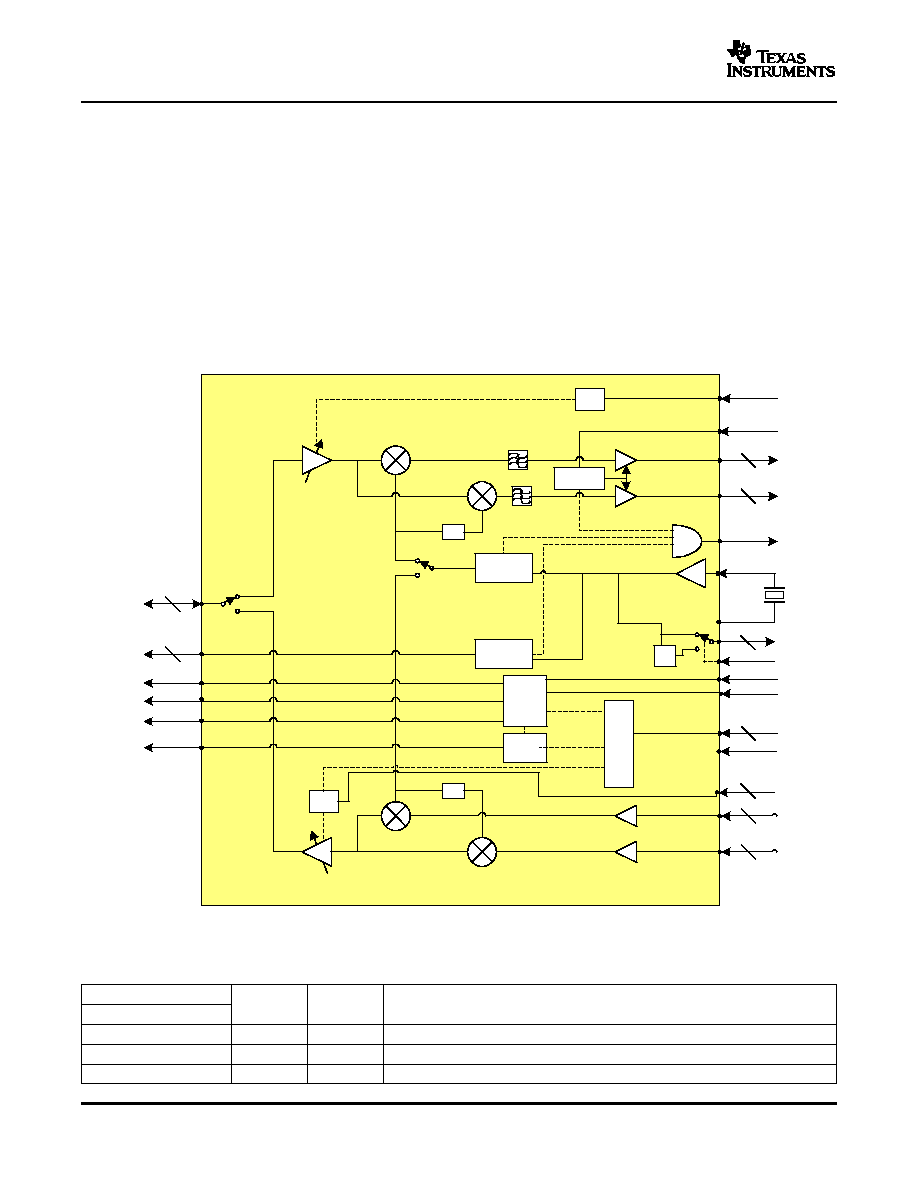
The TRF2432 is a fully integrated IQ transceiver specifically for use in 802.11 applications. The TRF2432 is
designed to perform the IQ conversion at 374MHz IF as well as provide an RFLO and control logic to a TI RFFE
(Radio Frequency Front End). The TRF2432 uses a common IF frequency for both bands, which eliminates the
need for an additional IF filter in dual band applications. The TRF2432 has an internal IQ DC offset calibration
function for the receive IQ interface. Combined with a TI integrated RFFE, the TRF2432 completes the TI WLAN
two-chip radio.
The TRF2432 incorporates all of the system blocks from the modem to the RFFE except for the IF filtering and
the reference crystal. The ASIC uniquely incorporates an internal PLL reference oscillator where only a crystal is
needed, and also provides a clock output for base-band/MAC ASICs. TRF2432 includes two synthesizers with
VCOs, IQ modulator, IQ demodulator, anti aliasing filters, IF amplifiers, receive AGC circuit, transmit power
control and serial interface.
Functional Block Diagram
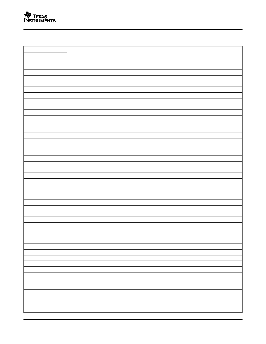
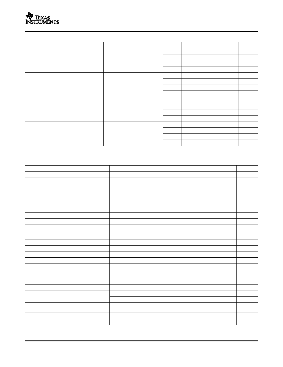
Table 1. TERMINAL FUNCTIONS
TERMINAL
I/O
TYPE
DESCRIPTION
NAME
NO.
RFPD
1
O
Analog
RFFE sleep output
PAPDA
2
O
Analog
PA band A select to RFFE
PAPDB
3
O
Analog
PA band B select to RFFE
2
www.ti.com
TRF2432
SLWS177A APRIL 2005 REVISED DECEMBER 2005
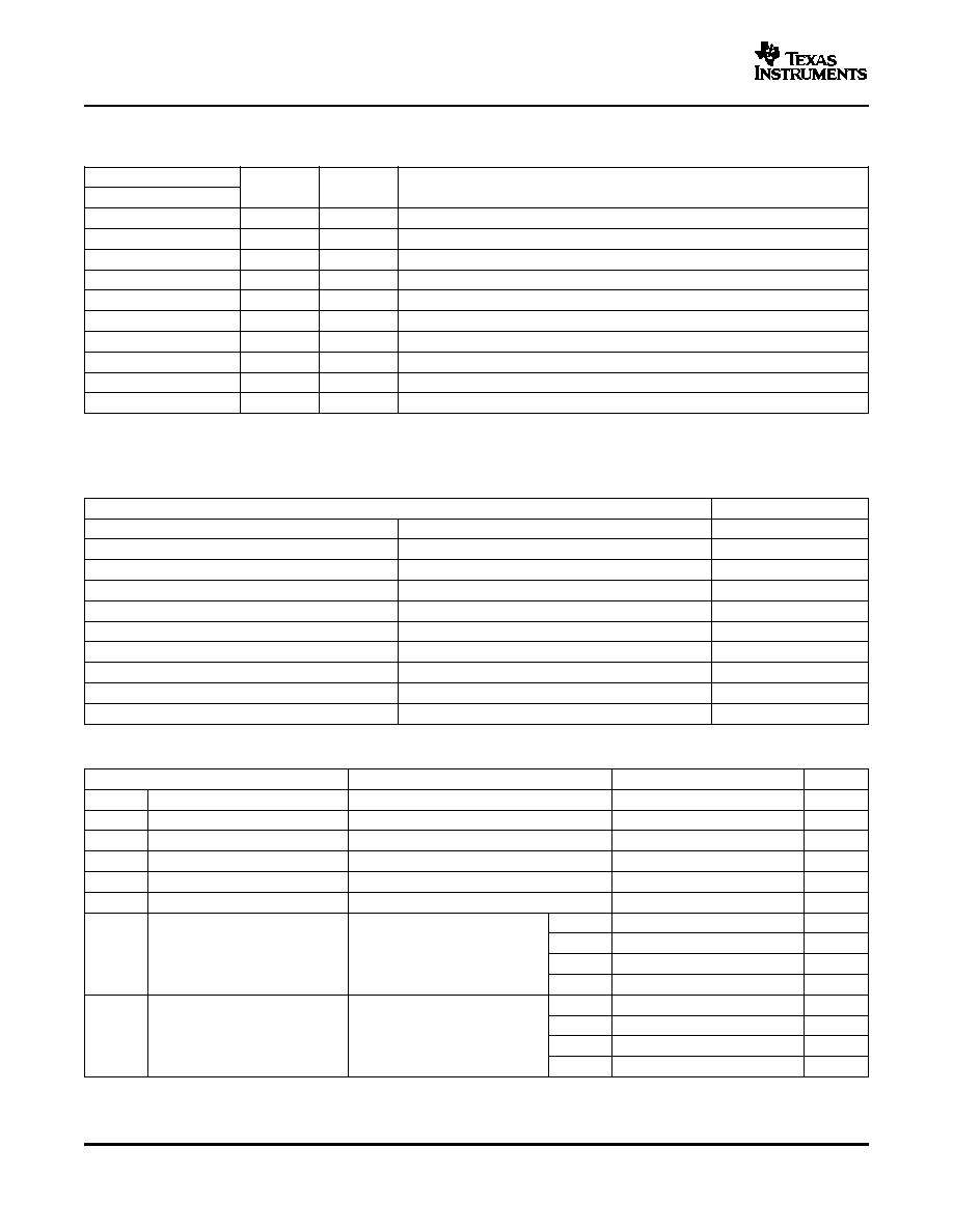
DEVICE INFORMATION (continued)
Table 1. TERMINAL FUNCTIONS (continued)
TERMINAL
I/O
TYPE
DESCRIPTION
NAME
NO.
ABSEL
4
O
Analog
A or B band select to RFFE
V+RFLO
5
I
Power
+3.3V Power Supply. RF VCO bias
GND
6
I
Analog
Connect to ground per suggested layout for normal operation
LON
7
O
RF Dif.
Positive going LO output
LOP
8
O
RF Dif.
Negative going LO output
GND
9
I
Analog
Connect to ground per suggested layout for normal operation
V+CP
10
I
Power
+3.3V Power Supply. Synthesizer Charge Pumps bias
RSVD2
11
-
-
Reserved. Leave open
RFLOBP
12
O
Analog
Bypass Capacitor for LO1 (RF)
RFLOTUN
13
I
Analog
VCO Synthesizer 1 (RF) Tuning port
RFLOCP
14
O
Analog
Synthesizer 1 (RF) Charge pump output
RSVD3
15
-
-
Reserved. Leave open
XTALO
16
I/O
Analog
Negative crystal connection
V+D
17
I
Power
+3.3V Power Supply. Digital Bias
CLKON
18
O
Digital
Negative going reference clock output (40,44,20 or 22MHz)
XTALBYP
19
O
Analog
Bypass Capacitor for crystal oscillator
CLKOP
20
O
Digital
Positive going reference clock output (40,44,20 or 22MHz)
V+CLK
21
I
Power
+3.3V Power Supply. Reference Clock Bias
CLK
22
I
Digital
Clock line of 3-wire serial bus
DATA
23
I
Digital
Data line of 3-wire serial bus
EN
24
I
Digital
Load enable line of 3-wire serial bus
A transition high in RX active mode initiates DC offset calibration. Low disables
CALEN
25
I
Digital
calibration circuit. Internal pull down
XTALI
26
I/O
Analog
Positive crystal connection. Also input for external XO reference
GND
27
I
Analog
Connect to ground per suggested layout for normal operation
REFDIV
28
I
Digital
Sets reference clock divider. Set HIGH to activate divide by 2. Internal pull down.
IFLOTUN
29
I
Analog
VCO Synthesizer 2 (IF) Tune port. CP2 Connected internally
IFLOBP
30
O
Analog
Bypass Capacitor for LO2 (IF)
RSVD1
31
-
-
Reserved. Leave open.
PA enable. HIGH enables RFFE PA. Enables PAPDA or PAPDB. Internal pull
PAEN
32
I
Digital
down.
TR
33
I
Digital
Transmit or Receive control line. TX=HIGH, RX=LOW. Internal pull down.
PE
34
I
Digital
Power enable. HIGH is enabled. Not defined internally.
STATUS
35
O
Digital
RF, IF and REF synthesizer lock detect and calibration status.
V+IFLO
36
I
Power
+3.3V Power Supply. IF VCO bias
GND
37
I
Analog
Connect to ground per suggested layout for normal operation
RXIN
38
O
Analog
Receiver in-phase negative going output.
RXIP
39
O
Analog
Receiver in-phase positive going output.
RXQN
40
O
Analog
Receiver quadrature negative going output.
RXQP
41
O
Analog
Receiver quadrature positive going output.
GND
42
I
Analog
Connect to ground per suggested layout for normal operation
TXQN
43
I
Analog
Transmitter quadrature negative going output.
TXQP
44
I
Analog
Transmitter quadrature positive going output.
TXIN
45
I
Analog
Transmitter in-phase negative going output.
TXIP
46
I
Analog
Transmitter in-phase positive going output.
3
www.ti.com
ABSOLUTE MAXIMUM RATINGS
DC CHARACTERISTICS
TRF2432
SLWS177A APRIL 2005 REVISED DECEMBER 2005
DEVICE INFORMATION (continued)
Table 1. TERMINAL FUNCTIONS (continued)
TERMINAL
I/O
TYPE
DESCRIPTION
NAME
NO.
RXCMADJ
47
I
Analog
Connect resistor to ground to adjust common mode output voltage
TXGC[4]
48
I
Digital
TX Gain Control bit 4 (MSB). Logic LOW induces 16dB Atten. Internal pull down.
TXGC[3]
49
I
Digital
TX Gain Control bit 3. Logic LOW induces 8dB Atten. Internal pull down.
TXGC[2]
50
I
Digital
TX Gain Control bit 2. Logic LOW induces 4dB Atten. Internal pull down.
TXGC[1]
51
I
Digital
TX Gain Control bit 1. Logic LOW induces 2dB Atten. Internal pull down.
TXGC[0]
52
I
Digital
TX Gain Control bit 0 (LSB). logic LOW induces 1dB Atten. Internal pull down.
RXAGC
53
I
Analog
Receiver automatic gain control pin.
IFN
54
I/O
RF Dif.
IF positive going input or output.
IFP
55
I/O
RF Dif.
IF negative going input or output.
V+TR
56
I
Power
+3.3V Power Supply. TX and RX IF amplifier bias.
over operating free-air temperature range (unless otherwise noted)
UNIT
DC supply voltage, V
CC
0 to 5.5 V
DC supply current, I
CC
600 mA
RF input power
Any port and any mode
+10 dBm
Digital input voltage, V
ID
-0.3 V to V
CC
+0.3 V
Analog input voltage, V
IA
0 to 3.6 V
Junction temperature, T
JC
125
°
C
Thermal resistance junction-to-case,
JC
25
°
C/W
Operating temperature, T
A
-20
°
C to +85
°
C
Storage temperature, T
stg
-40
°
C to +105
°
C
Lead temperature
40 sec maximum
+220
°
C
PARAMETER
TEST CONDITIONS
MIN
TYP
MAX
UNIT
V
CC
Supply votlage
Specification compliant
2.7
3.3
3.6
V
Transmit Mode Supply Current
TR = High, Active mode
100
125
mA
Receive Mode Supply Current
TR = Low, Active mode
90
110
mA
Idle Mode Supply Current
70
85
mA
Standby Mode Supply Current
10
15
mA
Sleep Mode Supply Current
10
µA
DC current, V+RFLO
V
CC
= 3.3 V, 0 < V+RFLO < V+TR Standby
0
+ 0.6V
Idle
0
Tx
11
Rx
11
DC current, V+CP
V+TR - 0.6V < V+CP < V+TR +
Standby
0
0.6V
Idle
0.6
Tx
0.6
Rx
0.6
4
www.ti.com
RECEIVER CHARACTERISTICS
TRF2432
SLWS177A APRIL 2005 REVISED DECEMBER 2005
DC CHARACTERISTICS (continued)
PARAMETER
TEST CONDITIONS
MIN
TYP
MAX
UNIT
DC current, V+D
V+TR - 0.6V < V+D < V+TR +
Standby
8.5
0.6V
Idle
50/30
Tx
50/30
Rx
50/30
DC current, V+CLK
V+TR - 0.6V < V+CLK < V+TR +
Standby
4
0.6V
Idle
4
Tx
4
Rx
4
DC current, V+IFLO
0 < V+IFLO < V+TR + 0.6V
Standby
0
Idle
0
Tx
8.5
Rx
8.5
DC current, V+TR
3.6 V max
Standby
0.35
Idle
0.35
Tx
33/21
Rx
20
T
A
= 25
°
C and V
CC
= 3.3 V (unless otherwise noted)
PARAMETER
TEST CONDITIONS
MIN
TYP
MAX
UNIT
f
IF
IF input frequency
374
MHz
Voltage gain
Gain control < 0.3 V
62
71
dB
Analog Gain Control Range
V
AGC
from .3 to 2.2V
55
dB
Gain Control Sensitivity
Monotonic.
-40
-50
dB/V
Gain Control Linearity
From linear
±
3
Gain settling time
Full range to within 0.5dB final gain
0.25
µs
setting
Output P
-1dB
-7
dBm
Output 3rd order intercept point
4.8
Vppd
Noise figure
From Full Gain to 40dB gain. Not to
7
dB
increase more than 1dB per 1dB of
gain change thereafter.
IQ differential impedance
I, Q outputs (0-11MHz)
100
Output load impedance
Single ended
2||10
k
||pF
Output swing
1000
mVpd
Input return loss
Measured into 200-
differential
9
dB
Output common mode voltage
Adjustable by one resistor to ground.
0.6
1.4
V
V
com
= 0.56 + 0.48
×
R
ADJ
, R
ADJ
is
k
I/Q gain mismatch
0 to 11 MHz band
0.1
0.5
dB
I/Q phase imbalance
0 to 11 MHz band
0.9
3
°
I/Q differential DC offset
After calibration. Min Gain
10
mV
Before calibration
50
mV
DC offset calibration time
With 40 MHz reference. See
32
µs
calibration instructions
LPF attenuation
25 MHz
20
25
dB
10.55 MHz
1
dB
5
Document Outline