Äîêóìåíòàöèÿ è îïèñàíèÿ www.docs.chipfind.ru
TPIC6B259
POWER LOGIC 8-BIT ADDRESSABLE LATCH
SLIS030 APRIL 1994 REVISED JULY 1995
1
POST OFFICE BOX 655303
·
DALLAS, TEXAS 75265
D
Low r
DS(on)
. . . 5
Typical
D
Avalanche Energy . . . 30 mJ
D
Eight Power DMOS-Transistor Outputs of
150-mA Continuous Current
D
500-mA Typical Current-Limiting Capability
D
Output Clamp Voltage . . . 50 V
D
Four Distinct Function Modes
D
Low Power Consumption
description
This power logic 8-bit addressable latch controls
open-drain DMOS-transistor outputs and is
designed for general-purpose storage
applications in digital systems. Specific uses
include working registers, serial-holding registers,
and decoders or demultiplexers. This is a multi-
functional device capable of storing single-line
data in eight addressable latches and 3-to-8
decoder or demultiplexer with active-low DMOS
outputs.
Four distinct modes of operation are selectable by
controlling the clear (CLR) and enable (G) inputs
as enumerated in the function table. In the
addressable-latch mode, data at the data-in (D)
terminal is written into the addressed latch. The
addressed DMOS-transistor output inverts the
data input with all unaddressed DMOS-transistor
outputs remaining in their previous states. In the
memory mode, all DMOS-transistor outputs
remain in their previous states and are unaffected
by the data or address inputs. To eliminate the
possibility of entering erroneous data in the latch,
enable G should be held high (inactive) while the
address lines are changing. In the 3-to-8 decoding
or demultiplexing mode, the addressed output is
inverted with respect to the D input and all other
outputs are off. In the clear mode, all outputs are off and unaffected by the address and data inputs. When data
is low for a given output, the DMOS-transistor output is off. When data is high, the DMOS-transistor output has
sink-current capability.
Outputs are low-side, open-drain DMOS transistors with output ratings of 50 V and 150-mA continuous
sink-current capability. Each output provides a 500-mA typical current limit at T
C
= 25
°
C. The current limit
decreases as the junction temperature increases for additional device protection.
The TPIC6B259 is characterized for operation over the operating case temperature range of 40
°
C to 125
°
C.
Copyright
©
1997, Texas Instruments Incorporated
PRODUCTION DATA information is current as of publication date.
Products conform to specifications per the terms of Texas Instruments
standard warranty. Production processing does not necessarily include
testing of all parameters.
1
2
3
4
5
6
7
8
9
10
20
19
18
17
16
15
14
13
12
11
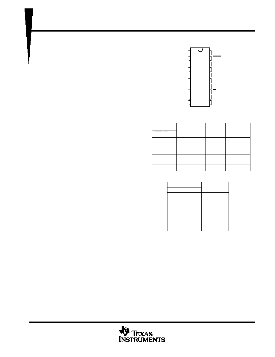
NC
V
CC
S0
DRAIN0
DRAIN1
DRAIN2
DRAIN3
S1
GND
GND
NC
CLR
D
DRAIN7
DRAIN6
DRAIN5
DRAIN4
G
S2
GND
DW OR N PACKAGE
(TOP VIEW)
OUTPUT OF
ADDRESSED
DRAIN
EACH
OTHER
DRAIN
INPUTS
FUNCTION
CLR G
FUNCTION TABLE
LATCH SELECTION TABLE
SELECT INPUTS
DRAIN
ADDRESSED
0
1
2
3
4
5
6
7
L
L
L
L
H
H
H
H
D
H
H
L
L
H
L
L
H
Qio
Qio
Qio
Qio
H
H
X
Memory
L
L
L
L
H
L
L
H
H
H
8-Line
Demultiplexer
L
H
X
H
H
Clear
Addressable
Latch
S2
S1
S0
L
L
H
H
L
L
H
H
L
H
L
H
L
H
L
H
NC No internal connection
H = high level, L = low level
PRODUCTION DATA information is current as of publication date.
Products conform to specifications per the terms of Texas Instruments
standard warranty. Production processing does not necessarily include
testing of all parameters.
TPIC6B259
POWER LOGIC 8-BIT ADDRESSABLE LATCH
SLIS030 APRIL 1994 REVISED JULY 1995
2
POST OFFICE BOX 655303
·
DALLAS, TEXAS 75265
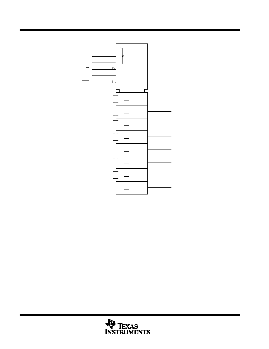
logic symbol
0
3
S0
8
S1
2
12
S2
G8
13
Z9
18
D
Z10
19
8M 0/7
9,0D
9,1D
9,2D
9,3D
9,4D
9,5D
9,6D
9,7D
10,0R
DRAIN0
4
DRAIN1
5
DRAIN2
6
DRAIN3
7
DRAIN4
14
DRAIN5
15
DRAIN6
16
DRAIN7
17
10,1R
10,2R
10,3R
10,4R
10,5R
10,6R
10,7R
G
CLR
This symbol is in accordance with ANSI/IEEE Std 91-1984 and IEC Publication 617-12.
TPIC6B259
POWER LOGIC 8-BIT ADDRESSABLE LATCH
SLIS030 APRIL 1994 REVISED JULY 1995
3
POST OFFICE BOX 655303
·
DALLAS, TEXAS 75265
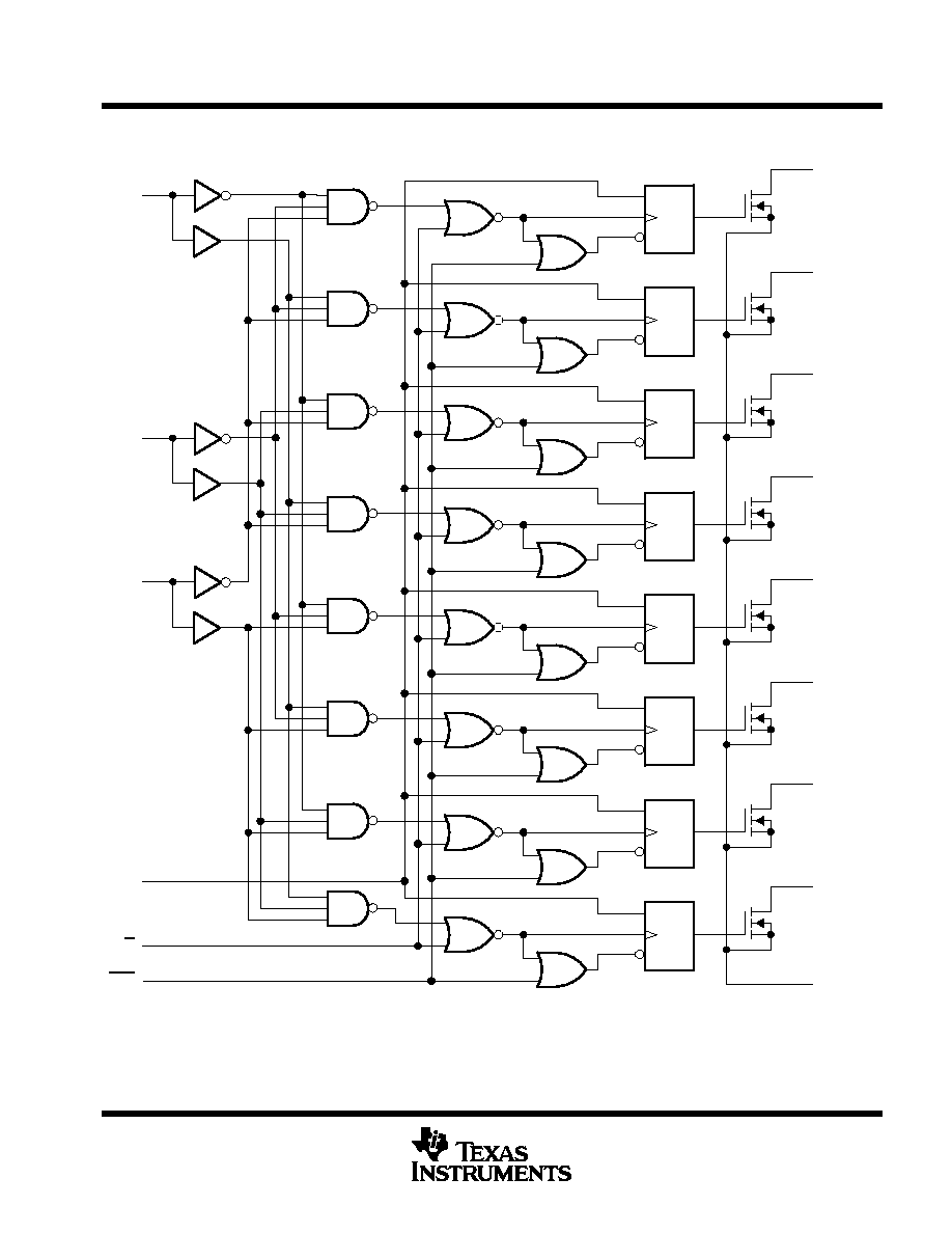
logic diagram (positive logic)
C1
S0
S2
S1
D
G
CLR
4
DRAIN0
5
DRAIN1
6
DRAIN2
7
DRAIN3
14
DRAIN4
15
DRAIN5
16
DRAIN6
17
DRAIN7
9,10,11
GND
3
12
8
18
13
19
D
CLR
C1
D
CLR
C1
D
CLR
C1
D
CLR
C1
D
CLR
C1
D
CLR
C1
D
CLR
C1
D
CLR
TPIC6B259
POWER LOGIC 8-BIT ADDRESSABLE LATCH
SLIS030 APRIL 1994 REVISED JULY 1995
4
POST OFFICE BOX 655303
·
DALLAS, TEXAS 75265
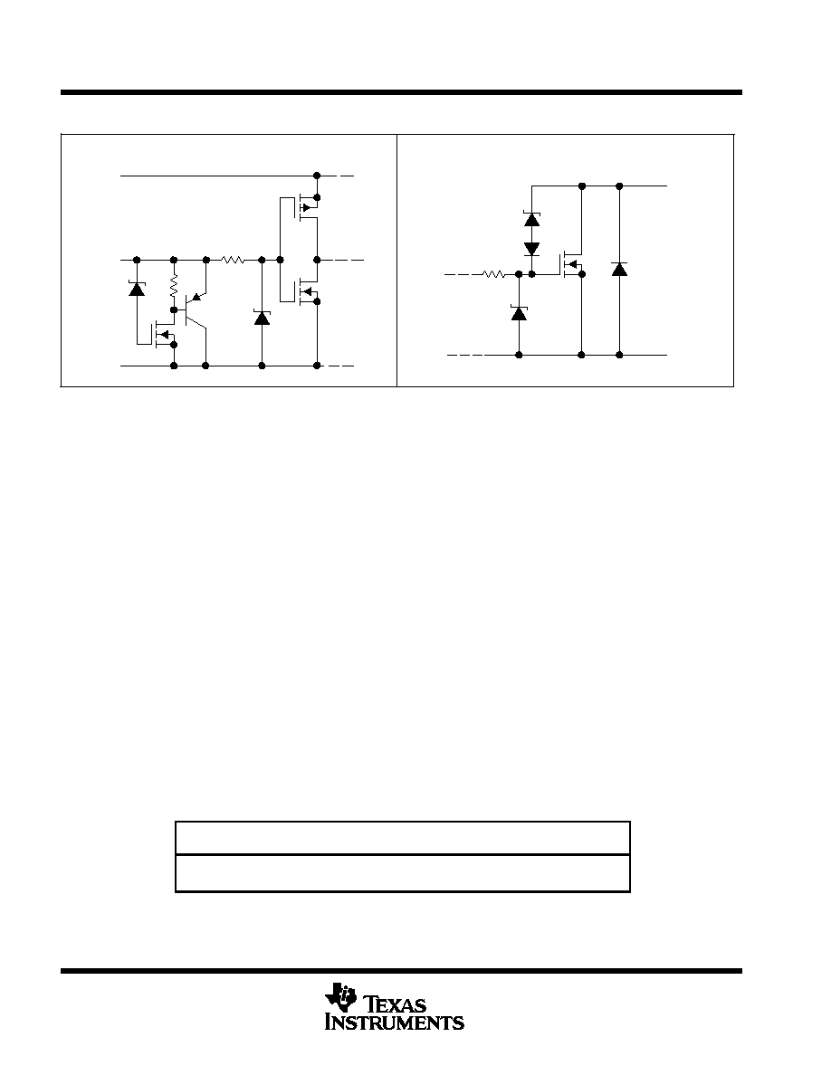
schematic of inputs and outputs
EQUIVALENT OF EACH INPUT
TYPICAL OF ALL DRAIN OUTPUTS
VCC
Input
GND
GND
DRAIN
50 V
20 V
25 V
12 V
absolute maximum ratings over the recommended operating case temperature range (unless
otherwise noted)
Logic supply voltage, V
CC
(see Note 1)
7 V
. . . . . . . . . . . . . . . . . . . . . . . . . . . . . . . . . . . . . . . . . . . . . . . . . . . . . . .
Logic input voltage range, V
I
0.3 V to 7 V
. . . . . . . . . . . . . . . . . . . . . . . . . . . . . . . . . . . . . . . . . . . . . . . . . . . . . . . .
Power DMOS drain-to-source voltage, V
DS
(see Note 2)
50 V
. . . . . . . . . . . . . . . . . . . . . . . . . . . . . . . . . . . . . . . .
Continuous source-to-drain diode anode current
500 mA
. . . . . . . . . . . . . . . . . . . . . . . . . . . . . . . . . . . . . . . . . . . .
Pulsed source-to-drain diode anode current (see Note 3)
1 A
. . . . . . . . . . . . . . . . . . . . . . . . . . . . . . . . . . . . . . . . .
Pulsed drain current, each output, all outputs on, I
D
, T
C
= 25
°
C (see Note 3)
500 mA
. . . . . . . . . . . . . . . . . . .
Continuous drain current, each output, all outputs on, I
D
,
T
C
= 25
°
C 150
mA
. . . . . . . . . . . . . . . . . . . . . . . . . . .
Peak drain current single output, I
DM
, T
C
= 25
°
C (see Note 3)
500 mA
. . . . . . . . . . . . . . . . . . . . . . . . . . . . . . . .
Single-pulse avalanche energy, E
AS
(see Figure 4)
30
mJ
. . . . . . . . . . . . . . . . . . . . . . . . . . . . . . . . . . . . . . . . . . .
Avalanche current, I
AS
(see Note 4)
500
mA
. . . . . . . . . . . . . . . . . . . . . . . . . . . . . . . . . . . . . . . . . . . . . . . . . . . . . .
Continuous total dissipation
See Dissipating Rating Table
. . . . . . . . . . . . . . . . . . . . . . . . . . . . . . . . . . . . . . . . . . .
Operating virtual junction temperature range, T
J
40
°
C to 150
°
C
. . . . . . . . . . . . . . . . . . . . . . . . . . . . . . . . . . . . .
Operating case temperature range, T
C
40
°
C to 125
°
C
. . . . . . . . . . . . . . . . . . . . . . . . . . . . . . . . . . . . . . . . . . . . .
Storage temperature range
65
°
C to 150
°
C
. . . . . . . . . . . . . . . . . . . . . . . . . . . . . . . . . . . . . . . . . . . . . . . . . . . . . . . .
Lead temperature 1,6 mm (1/16 inch) from case for 10 seconds
260
°
C
. . . . . . . . . . . . . . . . . . . . . . . . . . . . . . .
Stresses beyond those listed under "absolute maximum ratings" may cause permanent damage to the device. These are stress ratings only, and
functional operation of the device at these or any other conditions beyond those indicated under "recommended operating conditions" is not
implied. Exposure to absolute-maximum-rated conditions for extended periods may affect device reliability.
NOTES:
1. All voltage values are with respect to GND.
2. Each power DMOS source is internally connected to GND.
3. Pulse duration
100
µ
s and duty cycle
2%.
4. DRAIN supply voltage = 15 V, starting junction temperature (TJS) = 25
°
C, L = 200 mH, IAS = 0.5 A (see Figure 4).
DISSIPATION RATING TABLE
PACKAGE
TC
25
°
C
POWER RATING
DERATING FACTOR
ABOVE TC = 25
°
C
TC = 125
°
C
POWER RATING
DW
1389 mW
11.1 mW/
°
C
278 mW
N
1050 mW
10.5 mW/
°
C
263 mW
TPIC6B259
POWER LOGIC 8-BIT ADDRESSABLE LATCH
SLIS030 APRIL 1994 REVISED JULY 1995
5
POST OFFICE BOX 655303
·
DALLAS, TEXAS 75265
recommended operating conditions
MIN
MAX
UNIT
Logic supply voltage, VCC
4.5
5.5
V
High-level input voltage, VIH
0.85 VCC
V
Low-level input voltage, VIL
0.15 VCC
V
Pulsed drain output current, TC = 25
°
C, VCC = 5 V (see Notes 3 and 5)
500
500
mA
Setup time, D high before G
, tsu (see Figure 2)
20
ns
Hold time, D high after G
, th (see Figure 2)
20
ns
Pulse duration, tw (see Figure 2)
40
ns
Operating case temperature, TC
40
125
°
C
electrical characteristics, V
CC
= 5 V, T
C
= 25
°
C
(unless otherwise noted)
PARAMETER
TEST CONDITIONS
MIN
TYP
MAX
UNIT
V(BR)DSX
Drain-to-source breakdown
voltage
ID = 1 mA
50
V
VSD
Source-to-drain diode forward
voltage
IF = 100 mA
0.85
1
V
IIH
High-level input current
VCC = 5.5 V,
VI = VCC
1
µ
A
IIL
Low-level input current
VCC = 5.5 V,
VI = 0
1
µ
A
ICC
Logic supply current
VCC = 5 5 V
All outputs off
20
100
µ
A
ICC
Logic supply current
VCC = 5.5 V
All outputs on
150
300
µ
A
IN
Nominal current
VDS(on) = 0.5 V, IN = ID,
TC = 85
°
C,
See Notes 5, 6, and 7
90
mA
IDSX
Off state drain current
VDS = 40 V,
VCC = 5.5 V
0.1
5
µ
A
IDSX
Off-state drain current
VDS = 40 V,
VCC = 5.5 V,
TC = 125
°
C
0.15
8
µ
A
ID = 100 mA,
VCC = 4.5 V
4.2
5.7
rDS(on)
Static drain-to-source on-state
resistance
ID = 100 mA,
TC = 125
°
C
VCC = 4.5 V,
See Notes 5 and 6
and Figures 6 and 7
6.8
9.5
ID = 350 mA,
VCC = 4.5 V
5.5
8
switching characteristics, V
CC
= 5 V, T
C
= 25
°
C
PARAMETER
TEST CONDITIONS
MIN
TYP
MAX
UNIT
tPLH Propagation delay time, low-to-high-level output from D
150
ns
tPHL Propagation delay time, high-to-low-level output from D CL = 30 pF,
ID = 100 mA,
90
ns
tr
Rise time, drain output
L
,
D
,
See Figures 1, 2, and 8
200
ns
tf
Fall time, drain output
200
ns
ta
Reverse-recovery-current rise time
IF = 100 mA,
di/dt = 20 A/
µ
s,
100
ns
trr
Reverse-recovery time
F
µ
See Notes 5 and 6 and Figure 3
300
ns
NOTES:
3. Pulse duration
100
µ
s and duty cycle
2%.
5. Technique should limit TJ TC to 10
°
C maximum.
6. These parameters are measured with voltage-sensing contacts separate from the current-carrying contacts.
7. Nominal current is defined for a consistent comparison between devices from different sources. It is the current that produces a
voltage drop of 0.5 V at TC = 85
°
C.
TPIC6B259
POWER LOGIC 8-BIT ADDRESSABLE LATCH
SLIS030 APRIL 1994 REVISED JULY 1995
6
POST OFFICE BOX 655303
·
DALLAS, TEXAS 75265
thermal resistance
PARAMETER
TEST CONDITIONS
MIN
MAX
UNIT
R
JA
Thermal resistance junction to ambient
DW package
All 8 outputs with equal power
90
°
C/W
R
JA
Thermal resistance junction-to-ambient
N package
All 8 outputs with equal power
95
°
C/W
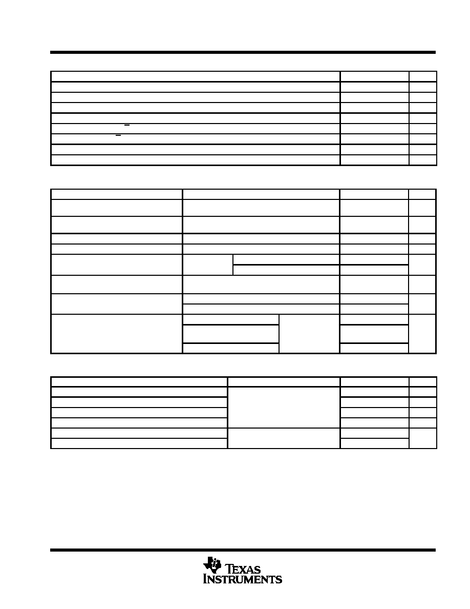
PARAMETER MEASUREMENT INFORMATION
TEST CIRCUIT
5 V
24 V
VCC
DRAIN
GND
CLR
RL = 235
Output
D
Word
Generator
(see Note A)
0 V
5 V
0.5 V
24 V
D
G
G
DRAIN5
CLR
VOLTAGE WAVEFORMS
S0
0 V
5 V
S1
0 V
5 V
S2
0 V
5 V
5 V
5 V
0 V
0 V
0.5 V
24 V
DRAIN3
S2
S1
S0
CL = 30 pF
(see Note B)
DUT
3
8
12
13
19
18
2
9, 10, 11
4 7,
14 17
ID
NOTES: A. The word generator has the following characteristics: tr
10 ns, tf
10 ns, tw = 300 ns, pulsed repetition rate (PRR) = 5 kHz,
ZO = 50
.
B. CL includes probe and jig capacitance.
Figure 1. Resistive-Load Test Circuit and Voltage Waveforms
TPIC6B259
POWER LOGIC 8-BIT ADDRESSABLE LATCH
SLIS030 APRIL 1994 REVISED JULY 1995
7
POST OFFICE BOX 655303
·
DALLAS, TEXAS 75265
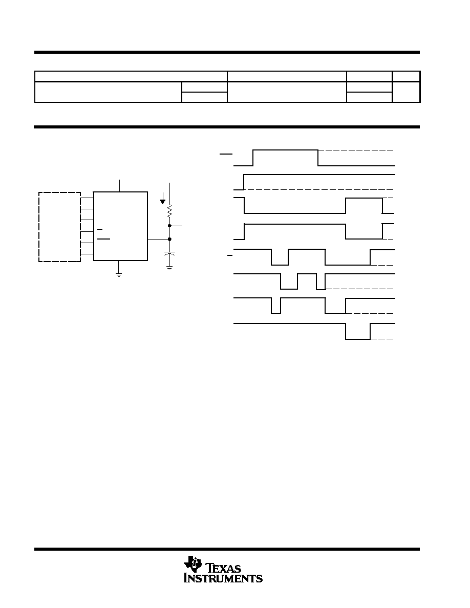
PARAMETER MEASUREMENT INFORMATION
SWITCHING TIMES
G
D
5 V
0 V
5 V
0 V
50%
Output
24 V
0.5 V
90%
10%
tPLH
tr
50%
90%
10%
tPHL
tf
5 V
0 V
50%
D
5 V
0 V
50%
50%
tsu
th
tw
INPUT SETUP AND HOLD WAVEFORMS
G
5 V
24 V
DUT
VCC
CLR
DRAIN
GND
D
235
ID
TEST CIRCUIT
Word
Generator
(see Note A)
G
CL = 30 pF
(see Note B)
Output
Word
Generator
(see Note A)
2
19
9, 10,11
13
18
4 7,
14 17
NOTES: A. The word generator has the following characteristics: tr
10 ns, tf
10 ns, tw = 300 ns, pulsed repetition rate (PRR) = 5 kHz,
ZO = 50
.
B. CL includes probe and jig capacitance.
Figure 2. Test Circuit, Switching Times, and Voltage Waveforms
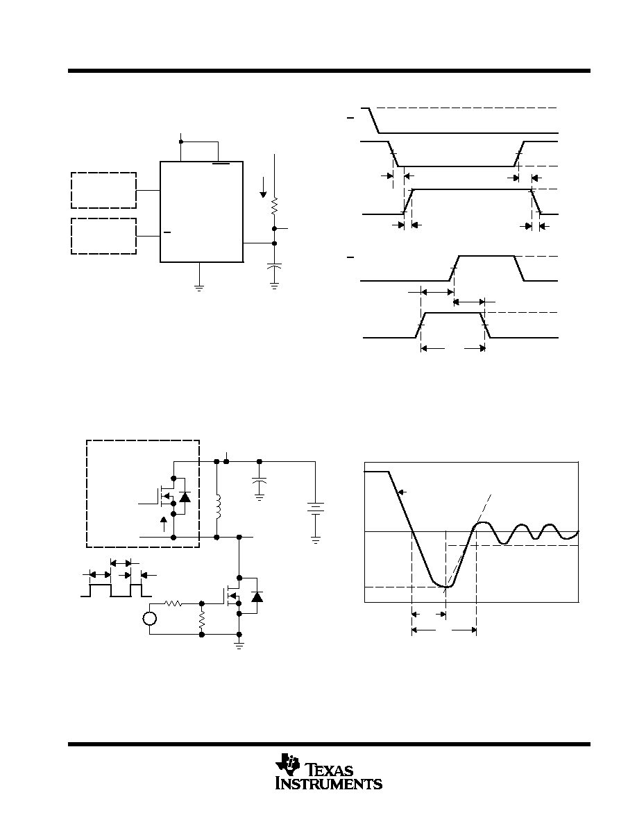
+
2500
µ
F
250 V
L = 1 mH
IF
(see Note A)
RG
VGG
(see Note B)
Driver
TP A
50
Circuit
Under
Test
DRAIN
25 V
t1
t3
t2
TP K
TEST CIRCUIT
0.1 A
IF
0
IRM
25% of IRM
ta
trr
di/dt = 20 A/
µ
s
CURRENT WAVEFORM
NOTES: A. The DRAIN terminal under test is connected to the TP K test point. All other terminals are connected together and connected to the
TP A test point.
B. The VGG amplitude and RG are adjusted for di/dt = 20 A/
µ
s. A VGG double-pulse train is used to set IF = 0.1 A, where t1 = 10
µ
s,
t2 = 7
µ
s, and t3 = 3
µ
s.
Figure 3. Reverse-Recovery-Current Test Circuit and Waveforms of Source-to-Drain Diode
TPIC6B259
POWER LOGIC 8-BIT ADDRESSABLE LATCH
SLIS030 APRIL 1994 REVISED JULY 1995
8
POST OFFICE BOX 655303
·
DALLAS, TEXAS 75265
PARAMETER MEASUREMENT INFORMATION
TEST CIRCUIT
5 V
15 V
VCC
DRAIN
GND
CLR
200 mH
VDS
D
Word
Generator
(see Note A)
G
DUT
10.5
9, 10, 11
tw
tav
IAS = 0.5 A
V(BR)DSX = 50 V
MIN
VOLTAGE AND CURRENT WAVEFORMS
Input
ID
VDS
See Note B
S0
S1
S2
3
8
12
19
18
13
ID
2
4 7,
14 17
5 V
0 V
NOTES: A. The word generator has the following characteristics: tr
10 ns, tf
10 ns, ZO = 50
.
B. Input pulse duration, tw, is increased until peak current IAS = 0.5 A.
Energy test level is defined as EAS = IAS
×
V(BR)DSX
×
tav/2 = 30 mJ.
Figure 4. Single-Pulse Avalanche Energy Test Circuit and Waveforms
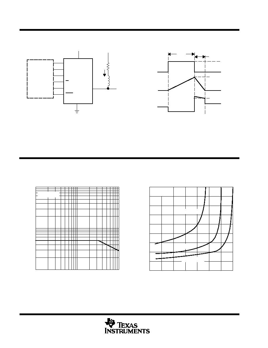
TYPICAL CHARACTERISTICS
2
1
10
4
0.1
0.2
1
0.4
2
10
4
0.2
0.1
0.4
I Peak
A
valanche
Current
A
AS
PEAK AVALANCHE CURRENT
vs
TIME DURATION OF AVALANCHE
tav Time Duration of Avalanche ms
TC = 25
°
C
10
8
4
2
0
6
0
100
200
300
400
14
12
16
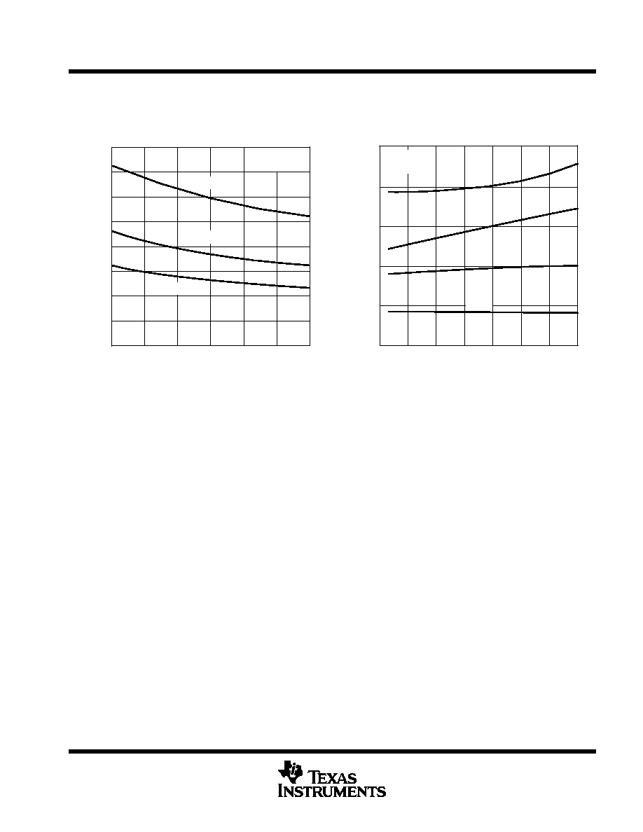
DRAIN-TO-SOURCE ON-STATE RESISTANCE
vs
DRAIN CURRENT
18
500
600
700
ID Drain Current mA
VCC = 5 V
See Note A
TC = 25
°
C
TC = 40
°
C
TC = 125
°
C
DS(on)
Drain-to-Source On-State Resistance
r
NOTE C: Technique should limit TJ TC to 10
°
C maximum.
Figure 5
Figure 6
TPIC6B259
POWER LOGIC 8-BIT ADDRESSABLE LATCH
SLIS030 APRIL 1994 REVISED JULY 1995
9
POST OFFICE BOX 655303
·
DALLAS, TEXAS 75265
TYPICAL CHARACTERISTICS
VCC Logic Supply Voltage V
STATIC DRAIN-TO-SOURCE ON-STATE RESISTANCE
vs
LOGIC SUPPLY VOLTAGE
DS(on)
Static Drain-to-Source On-State Resistance
r
4
3
1
0
4
4.5
5
5.5
5
7
8
6
6.5
7
6
2
TC = 125
°
C
TC = 25
°
C
TC = 40
°
C
ID = 100 mA
See Note A
Switching T
ime ns
SWITCHING TIME
vs
CASE TEMPERATURE
50
TC Case Temperature
°
C
ID = 100 mA
See Note A
200
150
100
50
250
300
tPHL
tPLH
tr
tf
25
0
25
50
75
100
125
Figure 7
Figure 8
NOTE D: Technique should limit TJ TC to 10
°
C maximum.
TPIC6B259
POWER LOGIC 8-BIT ADDRESSABLE LATCH
SLIS030 APRIL 1994 REVISED JULY 1995
10
POST OFFICE BOX 655303
·
DALLAS, TEXAS 75265
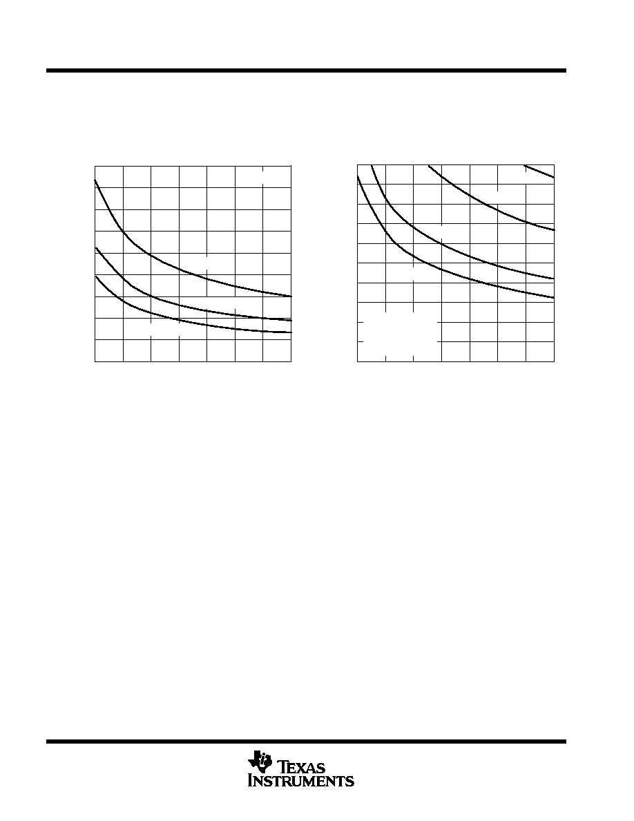
THERMAL INFORMATION
Maximum Continuous Drain Current
MAXIMUM CONTINUOUS
DRAIN CURRENT OF EACH OUTPUT
vs
NUMBER OF OUTPUTS CONDUCTING
SIMULTANEOUSLY
N Number of Outputs Conducting Simultaneously
of Each Output
A
DI
0
1
2
3
4
5
6
7
8
VCC = 5 V
TC = 25
°
C
TC = 125
°
C
0.45
0.4
0.35
0.3
0.25
0.2
0.15
0.1
0.05
Maximum Peak Drain Current of Each Output
A
MAXIMUM PEAK DRAIN CURRENT
OF EACH OUTPUT
vs
NUMBER OF OUTPUTS CONDUCTING
SIMULTANEOUSLY
D
N Number of Outputs Conducting Simultaneously
I
0.15
0.05
0.4
0
1
2
3
4
5
0.3
0.2
0.35
0.5
6
7
8
0.45
0.25
0.1
VCC = 5 V
TC = 25
°
C
d = tw/tperiod
= 1 ms/tperiod
d = 10%
d = 20%
d = 50%
d = 80%
TC = 100
°
C
Figure 9
Figure 10

IMPORTANT NOTICE
Texas Instruments and its subsidiaries (TI) reserve the right to make changes to their products or to discontinue
any product or service without notice, and advise customers to obtain the latest version of relevant information
to verify, before placing orders, that information being relied on is current and complete. All products are sold
subject to the terms and conditions of sale supplied at the time of order acknowledgement, including those
pertaining to warranty, patent infringement, and limitation of liability.
TI warrants performance of its semiconductor products to the specifications applicable at the time of sale in
accordance with TI's standard warranty. Testing and other quality control techniques are utilized to the extent
TI deems necessary to support this warranty. Specific testing of all parameters of each device is not necessarily
performed, except those mandated by government requirements.
CERTAIN APPLICATIONS USING SEMICONDUCTOR PRODUCTS MAY INVOLVE POTENTIAL RISKS OF
DEATH, PERSONAL INJURY, OR SEVERE PROPERTY OR ENVIRONMENTAL DAMAGE ("CRITICAL
APPLICATIONS"). TI SEMICONDUCTOR PRODUCTS ARE NOT DESIGNED, AUTHORIZED, OR
WARRANTED TO BE SUITABLE FOR USE IN LIFE-SUPPORT DEVICES OR SYSTEMS OR OTHER
CRITICAL APPLICATIONS. INCLUSION OF TI PRODUCTS IN SUCH APPLICATIONS IS UNDERSTOOD TO
BE FULLY AT THE CUSTOMER'S RISK.
In order to minimize risks associated with the customer's applications, adequate design and operating
safeguards must be provided by the customer to minimize inherent or procedural hazards.
TI assumes no liability for applications assistance or customer product design. TI does not warrant or represent
that any license, either express or implied, is granted under any patent right, copyright, mask work right, or other
intellectual property right of TI covering or relating to any combination, machine, or process in which such
semiconductor products or services might be or are used. TI's publication of information regarding any third
party's products or services does not constitute TI's approval, warranty or endorsement thereof.
Copyright
©
2000, Texas Instruments Incorporated