
SN75LP1185
LOW-POWER MULTIPLE RS-232 DRIVERS AND RECEIVERS
SLLS335 ş JANUARY 1999
1
POST OFFICE BOX 655303
Ě
DALLAS, TEXAS 75265
D
Single-Chip TIA/EIA-232-F Interface for
IBM
TM
PC/AT
TM
Serial Port
D
Designed to Transmit and Receive 4-
Á
s
Pulses (Equivalent to 256 kbit/s)
D
Less Than 21-mW Power Consumption
D
Wide Supply-Voltage Range, 4.75 V to 15 V
D
Driver Output Slew Rates Are Internally
Controlled to 30 V/
Á
s Max
D
Receiver Input Hysteresis, 1000 mV Typ
D
TIA/EIA-232-F Bus-Pin ESD Protection
Exceeds:
ş 15-kV, Human-Body Model
ş IEC1000-4-2 Level-4 Compliant
D
Three Drivers and Five Receivers Meet or
Exceed the Requirements of TIA/EIA-232-F
and ITU V.28
D
Complements the SN75LP196
D
Designed to Replace the Industry-Standard
SN75185 and SN75C185 With the Same
Flow-Through Pinout
D
Package Options Include Plastic
Small-Outline (DW), Shrink Small-Outline
(DB), Thin Shrink Small-Outline (PW), and
Dual-In-Line (N) Packages
description
The SN75LP1185 is a low-power bipolar device containing three drivers and five receivers with 15 kV of ESD
protection on the bus pins with respect to each other. Bus pins are defined as those pins that tie directly to the
serial-port connector, including GND. The pinout matches the flow-through design of the industry-standard
SN75185 and SN75C185. The flow-through pinout of the SN75LP1185 allows easy interconnection of the
UART and serial-port connector of the IBM PC/AT and compatibles. The SN75LP1185 provides a rugged,
low-cost solution for this function with the combination of the bipolar processing and 15 kV of ESD protection.
The SN75LP1185 has internal slew-rate control to provide a maximum rate of change in the output signal of
30 V/
Á
s. The driver output swing is nominally clamped at
▒
6 V to enable the higher data rates associated with
this device and to reduce EMI emissions. Even though the driver outputs are clamped, they can handle voltages
up to
▒
15 V without damage. All the logic inputs can accept 3.3-V or 5-V input signals.
The SN75LP1185 complies with the requirements of TIA/EIA-232-F and ITU V.28. These standards are for data
interchange between a host computer and peripheral at signaling rates up to 20 kbit/s. The switching speeds
of the SN75LP1185 support rates up to 256 kbit/s.
The SN75LP1185 is characterized for operation from 0
░
C to 70
░
C.
Copyright
ę
1999, Texas Instruments Incorporated
PRODUCTION DATA information is current as of publication date.
Products conform to specifications per the terms of Texas Instruments
standard warranty. Production processing does not necessarily include
testing of all parameters.
Please be aware that an important notice concerning availability, standard warranty, and use in critical applications of
Texas Instruments semiconductor products and disclaimers thereto appears at the end of this data sheet.
IBM and PC/AT are trademarks of International Business Machines Corporation.
V
DD
RA1
RA2
RA3
DY1
DY2
RA4
DY3
RA5
V
SS
V
CC
RY1
RY2
RY3
DA1
DA2
RY4
DA3
RY5
GND
1
2
3
4
5
6
7
8
9
10
20
19
18
17
16
15
14
13
12
11
DB, DW, N, OR PW PACKAGE
(TOP VIEW)

SN75LP1185
LOW-POWER MULTIPLE RS-232 DRIVERS AND RECEIVERS
SLLS335 ş JANUARY 1999
2
POST OFFICE BOX 655303
Ě
DALLAS, TEXAS 75265
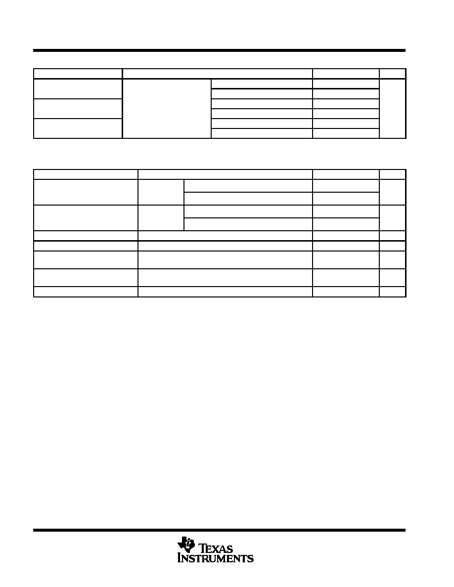
Function Tables
DRIVER
INPUT
DA
OUTPUT
DY
H
L
L
H
Open
L
RECEIVER
INPUT
RA
OUTPUT
RY
H
L
L
H
Open
H
logic diagram (positive logic)
2
3
4
5
6
7
8
9
19
18
17
16
15
14
13
12
RA1
RA2
RA3
DY1
DY2
RA4
DY3
RA5
RY1
RY2
RY3
DA1
DA2
RY4
DA3
RY5
SN75LP1185
LOW-POWER MULTIPLE RS-232 DRIVERS AND RECEIVERS
SLLS335 ş JANUARY 1999
3
POST OFFICE BOX 655303
Ě
DALLAS, TEXAS 75265
absolute maximum ratings over operating free-air temperature range (unless otherwise noted)
Positive supply-voltage range (see Note 1): V
CC
ş0.5 V to 7 V
. . . . . . . . . . . . . . . . . . . . . . . . . . . . . . . . . . . . . . .
V
DD
ş0.5 V to 15 V
. . . . . . . . . . . . . . . . . . . . . . . . . . . . . . . . . . . . . .
Negative supply-voltage range, V
SS
(see Note 1)
0.5 V to ş15 V
. . . . . . . . . . . . . . . . . . . . . . . . . . . . . . . . . . . . . .
Input-voltage range, V
I
: Receiver (RA)
ş30 V to 30 V
. . . . . . . . . . . . . . . . . . . . . . . . . . . . . . . . . . . . . . . . . . . . . . . .
Driver (DA)
ş0.5 V to V
CC
+ 0.4 V
. . . . . . . . . . . . . . . . . . . . . . . . . . . . . . . . . . . . . . . . . . . .
Output-voltage range, V
O
: Receiver (RY)
ş0.5 V to 6 V
. . . . . . . . . . . . . . . . . . . . . . . . . . . . . . . . . . . . . . . . . . . . . .
Driver (DY)
ş15 V to 15 V
. . . . . . . . . . . . . . . . . . . . . . . . . . . . . . . . . . . . . . . . . . . . . . . .
Electrostatic discharge: Bus pins (human-body model) (see Note 2)
Class 3: 15 kV
. . . . . . . . . . . . . . . . . . . . .
Bus pins (machine model)
500 V
. . . . . . . . . . . . . . . . . . . . . . . . . . . . . . . . . . . . . . . . . . . .
Bus pins (IEC1000-4-2, contact)
8 kV
. . . . . . . . . . . . . . . . . . . . . . . . . . . . . . . . . . . . . . . .
All pins (human-body model) (see Note 2)
Class 3: 5 kV
. . . . . . . . . . . . . . . . . . . . . . . .
All pins (machine model)
400 V
. . . . . . . . . . . . . . . . . . . . . . . . . . . . . . . . . . . . . . . . . . . . . .
Package thermal impedance,
JA
(see Note 3): DB package
115
░
C/W
. . . . . . . . . . . . . . . . . . . . . . . . . . . . . . . .
DW package
97
░
C/W
. . . . . . . . . . . . . . . . . . . . . . . . . . . . . . . . .
N package
67
░
C/W
. . . . . . . . . . . . . . . . . . . . . . . . . . . . . . . . . . .
PW package
128
░
C/W
. . . . . . . . . . . . . . . . . . . . . . . . . . . . . . . .
Storage temperature range, T
stg
65
░
C to 150
░
C
. . . . . . . . . . . . . . . . . . . . . . . . . . . . . . . . . . . . . . . . . . . . . . . . . . . . .
Lead temperature 1,6 mm (1/16 inch) from case for 10 seconds
260
░
C
. . . . . . . . . . . . . . . . . . . . . . . . . . . . . . . .
Stresses beyond those listed under "absolute maximum ratings" may cause permanent damage to the device. These are stress ratings only, and
functional operation of the device at these or any other conditions beyond those indicated under "recommended operating conditions" is not
implied. Exposure to absolute-maximum-rated conditions for extended periods may affect device reliability.
NOTES:
1. All voltage values are with respect to network ground terminal, unless otherwise noted.
2. Per MIL-STD-883, Method 3015.7
3. The package thermal impedance is calculated in accordance with JESD 51, except for through-hole packages, which use a trace
length of zero.
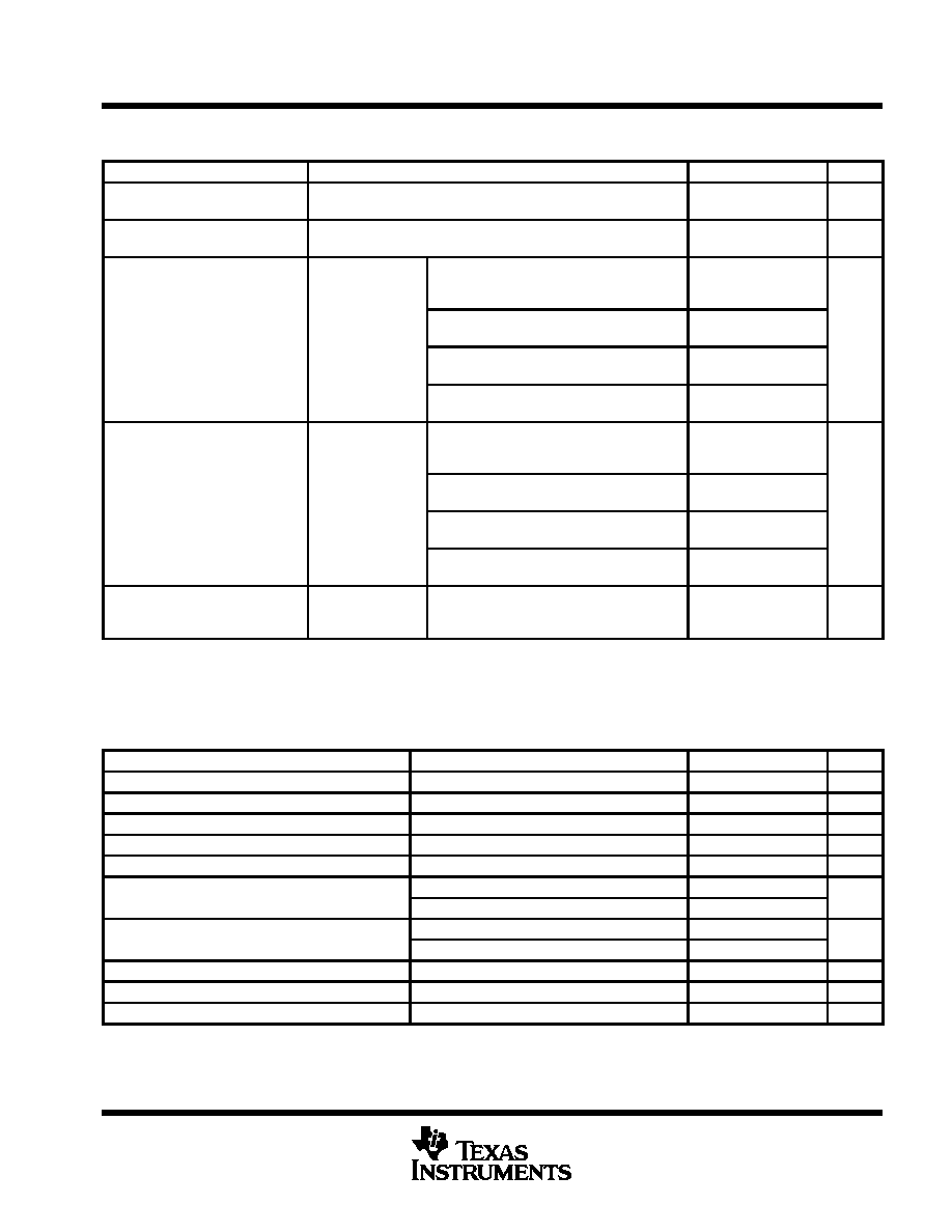
recommended operating conditions
MIN
NOM
MAX
UNIT
VCC
Supply voltage (see Note 4)
4.75
5
5.25
V
VDD
Supply voltage (see Note 5)
9
12
15
V
VSS
Supply voltage (see Note 5)
ş9
ş12
ş15
V
VIH
High-level input voltage
DA
2
V
VIL
Low-level input voltage
DA
0.8
V
VI
Receiver input voltage
RA
ş25
25
V
IOH
High-level output current
RY
ş1
mA
IOL
Low-level output current
RY
2
mA
TA
Operating free-air temperature
0
70
░
C
NOTES:
4. VCC cannot be greater than VDD.
5. The device operates down to VDD = VCC and |VSS| = VCC, but supply currents increase and other parameters may vary slightly from
the data sheet limits.
SN75LP1185
LOW-POWER MULTIPLE RS-232 DRIVERS AND RECEIVERS
SLLS335 ş JANUARY 1999
4
POST OFFICE BOX 655303
Ě
DALLAS, TEXAS 75265
supply currents over the recommended operating conditions (unless otherwise noted)
PARAMETER
TEST CONDITIONS
MIN
TYP
MAX
UNIT
Supply current for VCC ICC
VDD = 9 V,
VSS = ş9 V
1000
Supply current for VCC, ICC
VDD = 12 V,
VSS = ş12 V
1000
Supply current for VDD IDD
No load,
All inputs at minimum VOH or
VDD = 9 V,
VSS = ş9 V
800
Á
A
Supply current for VDD, IDD
All in uts at minimum VOH or
maximum VOL
VDD = 12 V,
VSS = ş12 V
800
Á
A
Supply current for VSS ISS
maximum VOL
VDD = 9 V,
VSS = ş9 V
ş625
Supply current for VSS, ISS
VDD = 12 V,
VSS = ş12 V
ş625
driver electrical characterisitics over the recommended operating conditions (unless otherwise
noted)
PARAMETER
TEST CONDITIONS
MIN
TYP
MAX
UNIT
VOH
High level output voltage
VIL = 0.8 V,
RL 3 k
VDD = 9 V,
VSS = ş9 V
5
5.8
6.6
V
VOH
High-level output voltage
RL = 3 k
,
See Figure 1
VDD = 12 V,
VSS = ş12 V,
See Note 6
5
5.8
6.6
V
VOL
Low level output voltage
VIH = 2 V,
RL 3 k
VDD = 9 V,
VSS = ş9 V
ş5
ş5.8
ş6.9
V
VOL
Low-level output voltage
RL = 3 k
,
See Figure 1
VDD = 12 V,
VSS = ş12 V,
See Note 6
ş5
ş5.9
ş6.9
V
IIH
High-level input current
VI at VCC
1
Á
A
IIL
Low-level input current
VI at GND
ş1
Á
A
IOS(H)
Short-circuit
high-level output current
VO = GND or VSS,
See Figure 2 and Note 7
ş30
ş55
mA
IOS(L)
Short-circuit
low-level output current
VO = GND or VDD,
See Figure 2 and Note 7
30
55
mA
ro
Output resistance
VDD = VSS = VCC = 0,
VO = 2 V
300
NOTES:
6. Maximum output swing is nominally clamped at
▒
6 V to enable the higher data rates associated with this device and to reduce EMI
emissions. The driver outputs may slightly exceed the maximum output voltage over the full VCC and temperature ranges.
7. Not more than one output should be shorted at one time.
SN75LP1185
LOW-POWER MULTIPLE RS-232 DRIVERS AND RECEIVERS
SLLS335 ş JANUARY 1999
5
POST OFFICE BOX 655303
Ě
DALLAS, TEXAS 75265
driver switching characteristics over recommended operating free-air temperature range (unless
otherwise noted)
PARAMETER
TEST CONDITIONS
MIN
TYP
MAX
UNIT
tPHL
Propagation delay time,
high- to low-level output
RL = 3 k
to 7 k
, CL = 15 pF, See Figure 1
300
800
1600
ns
tPLH
Propagation delay time,
low- to high-level output
RL = 3 k
to 7 k
, CL = 15 pF, See Figure 1
300
800
1600
ns
VCC = 5 V,
Using VTR = 10%-to-90% transition region,
Driver speed = 250 kbit/s, CL = 15 pF,
See Note 8
375
2240
tTLH
Transition time,
low to high level output
CC
VDD = 12 V,
VSS = ş12 V,
RL 3 k
to 7 k
Using VTR =
▒
3 V transition region,
Driver speed = 250 kbit/s, CL = 15 pF
200
1500
ns
TLH
low- to high-level output
RL = 3 k
to 7 k
,
See Figure 1 and
Note 9
Using VTR =
▒
2 V transition region,
Driver speed = 250 kbit/s, CL = 15 pF
133
1000
Note 9
Using VTR =
▒
3 V transition region,
Driver speed = 125 kbit/s, CL = 2500 pF
2750
VCC = 5 V,
Using VTR = 10%-to-90% transition region,
Driver speed = 250 kbit/s, CL = 15 pF,
See Note 8
375
2240
tTHL
Transition time,
high to low level output
CC
VDD = 12 V,
VSS = ş12 V,
RL 3 k
to 7 k
Using VTR =
▒
3 V transition region,
Driver speed = 250 kbit/s, CL = 15 pF
200
1500
ns
THL
high- to low-level output
RL = 3 k
to 7 k
,
See Figure 1 and
Note 9
Using VTR =
▒
2 V transition region,
Driver speed = 250 kbit/s, CL = 15 pF
133
1000
Note 9
Using VTR =
▒
3 V transition region,
Driver speed = 125 kbit/s, CL = 2500 pF
2750
SR
Output slew rate
VCC = 5 V,
VDD = 12 V,
VSS = ş12 V
Using VTR =
▒
3 V transition region,
Driver speed = 0 to 250 kbit/s, CL = 15 pF
4
20
30
V/
Á
s
NOTES:
8. Equivalent to the SN75C185. The SN75LP1185 output-voltage swing is clamped to about 70% of the typical SN75C185
output-voltage swing, and the specified limits reflect the reduced output swing.
9. Maximum output swing is limited to
▒
6 V to enable the higher data rates associated with this device and to reduce EMI emissions.
receiver electrical characteristics over recommended operating free-air temperature range
(unless otherwise noted)
PARAMETER
TEST CONDITIONS
MIN
TYP
MAX
UNIT
VIT+
Positive-going input threshold voltage
See Figure 3
1.6
2
2.55
V
VITş
Negative-going input threshold voltage
See Figure 3
0.6
1
1.45
V
VHYS
Input hysteresis, VIT+ VITş
See Figure 3
600
1000
mV
VOH
High-level output voltage
IOH = ş1 mA
2.5
3.9
V
VOL
Low-level output voltage
IOL = 2 mA
0.33
0.5
V
IIH
High level input current
VI = 3 V
0.43
0.6
1
mA
IIH
High-level input current
VI = 25 V
3.6
5.1
8.3
mA
IIL
Low level input current
VI = ş3 V
ş0.43
ş0.6
ş1
mA
IIL
Low-level input current
VI = ş25 V
ş3.6
ş5.1
ş8.3
mA
IOS(H)
Short-circuit high-level output current
VO = 0,
See Figure 5 and Note 7
ş20
mA
IOS(L)
Short-circuit low-level output current
VO = VCC,
See Figure 5 and Note 7
20
mA
RIN
Input resistance
VI =
▒
3 V to
▒
25 V
3
5
7
k
NOTE 7: Not more than one output should be shorted at one time.