Äîêóìåíòàöèÿ è îïèñàíèÿ www.docs.chipfind.ru
SN75146
DUAL DIFFERENTIAL LINE RECEIVER
SLLS015B FEBRUARY 1986 REVISED MAY 1995
1
POST OFFICE BOX 655303
·
DALLAS, TEXAS 75265
D
Meets or Exceeds the Requirements of
ANSI EIA / TIA-422-B and -423-B
D
Meets or Exceeds the Requirements of
ANSI EIA / TIA-232-E and ITU
Recommendation V.28 With External
Components
D
Meets Federal Standards 1020 and 1030
D
Built-in 5-MHz Low-Pass Filter
D
Operates From Single 5-V Power Supply
D
Wide Common-Mode Voltage Range
D
High Input Impedance
D
TTL-Compatible Outputs
D
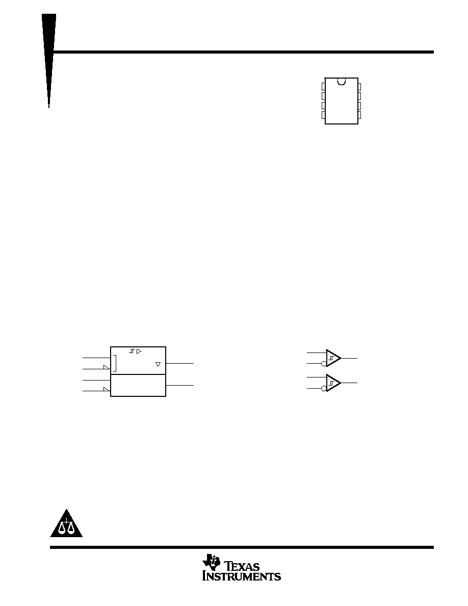
8-Pin Dual-in-Line Package
D
Pinout Compatible With the
µ
A9637 and
µ
A9639
description
The SN75146 is a dual differential line receiver designed to meet ANSI Standards EIA / TIA-422-B and -423-B.
The receiver is designed to have a constant impedance with input voltages of
±
3 V to
±
25 V allowing it to meet
the requirements of EIA / TIA-232-E and ITU recommendation V.28 with the addition of an external bias resistor.
This receiver is designed for low-speed operation below 355 kHz and has a built-in 5-MHz low-pass filter to
attenuate high-frequency noise. The inputs are compatible with either a single-ended or a differential line
system and the outputs are TTL compatible. This device operates from a single 5-V power supply and is
supplied in both the 8-pin dual-in-line and small-outline packages.
The SN75146 is characterized for operation from 0
°
C to 70
°
C.
logic symbol
5
6
7
8
2IN
2IN +
1IN
1IN +
2OUT
1OUT
3
2
This symbol is in accordance with ANSI/IEEE Std 91-1984 and
IEC Publication 617-12.
logic diagram
2OUT
1OUT
5
6
7
8
2IN
2IN +
1IN
1IN +
3
2
Copyright
©
1995, Texas Instruments Incorporated
PRODUCTION DATA information is current as of publication date.
Products conform to specifications per the terms of Texas Instruments
standard warranty. Production processing does not necessarily include
testing of all parameters.
Please be aware that an important notice concerning availability, standard warranty, and use in critical applications of
Texas Instruments semiconductor products and disclaimers thereto appears at the end of this data sheet.
1
2
3
4
8
7
6
5
V
CC
1OUT
2OUT
GND
1IN +
1IN
2IN +
2IN
D OR P PACKAGE
(TOP VIEW)
THE SN75146 IS NOT RECOMMENDED
FOR NEW DESIGNS.
SN75146
DUAL DIFFERENTIAL LINE RECEIVER
SLLS015B FEBRUARY 1986 REVISED MAY 1995
2
POST OFFICE BOX 655303
·
DALLAS, TEXAS 75265
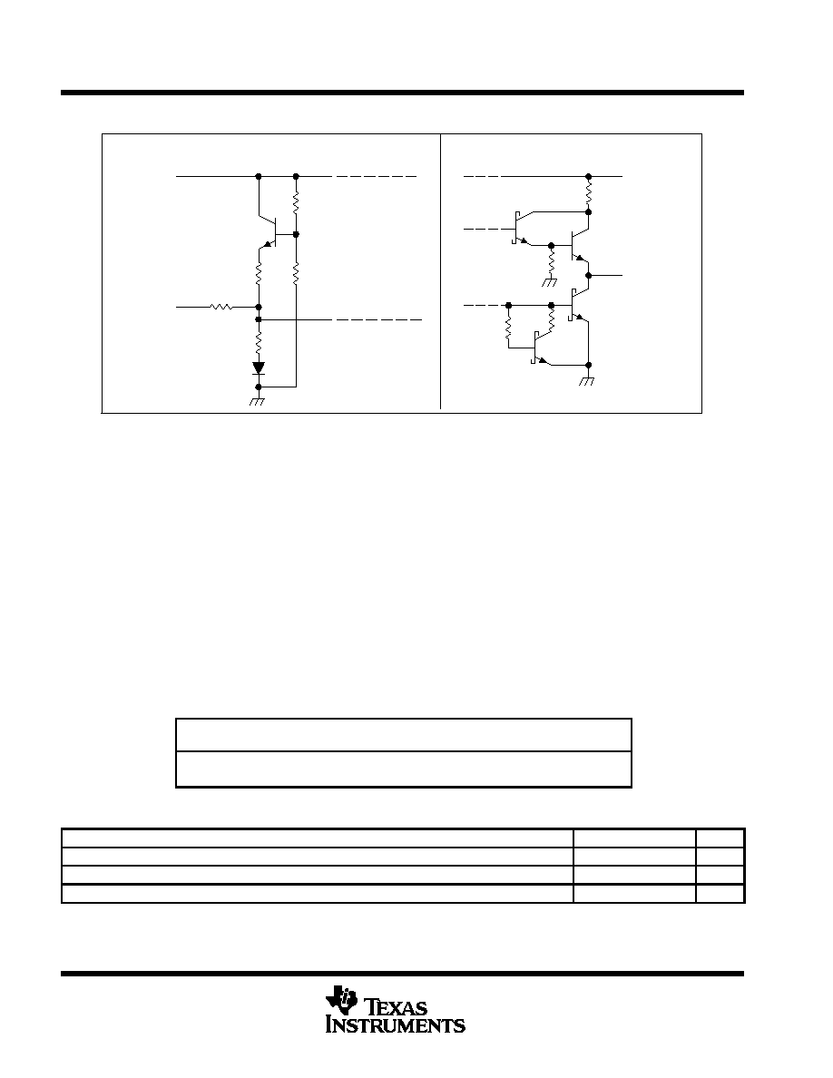
schematics of inputs and outputs
VCC
Input
740
NOM
7.4 k
NOM
7.41 R1
R1
740
NOM
EQUIVALENT OF EACH INPUT
TYPICAL OF ALL OUTPUTS
VCC
Output
50
NOM
absolute maximum ratings over operating free-air temperature range (unless otherwise noted)
Supply voltage range, V
CC
(see Note 1)
0.5 V to 7 V
. . . . . . . . . . . . . . . . . . . . . . . . . . . . . . . . . . . . . . . . . . . . . .
Input voltage, V
I
±
25 V
. . . . . . . . . . . . . . . . . . . . . . . . . . . . . . . . . . . . . . . . . . . . . . . . . . . . . . . . . . . . . . . . . . . . . . . . . .
Differential input voltage, V
ID
(see Note 2)
±
25 V
. . . . . . . . . . . . . . . . . . . . . . . . . . . . . . . . . . . . . . . . . . . . . . . . . . .
Output voltage range, V
O
(see Note 1)
0.5 V to 5.5 V
. . . . . . . . . . . . . . . . . . . . . . . . . . . . . . . . . . . . . . . . . . . . . .
Low-level output current, I
OL
50
mA
. . . . . . . . . . . . . . . . . . . . . . . . . . . . . . . . . . . . . . . . . . . . . . . . . . . . . . . . . . . . . .
Continuous total dissipation
See Dissipation Rating Table
. . . . . . . . . . . . . . . . . . . . . . . . . . . . . . . . . . . . . . . . . . . .
Operating free-air temperature range, T
A
0
°
C to 70
°
C
. . . . . . . . . . . . . . . . . . . . . . . . . . . . . . . . . . . . . . . . . . . . . .
Storage temperature range, T
stg
65
°
C to 150
°
C
. . . . . . . . . . . . . . . . . . . . . . . . . . . . . . . . . . . . . . . . . . . . . . . . . .
Lead temperature 1,6 mm (1/16 inch) from case for 10 seconds
260
°
C
. . . . . . . . . . . . . . . . . . . . . . . . . . . . . . .
Stresses beyond those listed under "absolute maximum ratings" may cause permanent damage to the device. These are stress ratings only, and
functional operation of the device at these or any other conditions beyond those indicated under "recommended operating conditions" is not
implied. Exposure to absolute-maximum-rated conditions for extended periods may affect device reliability.
NOTES:
1. All voltage values, except differential input voltage, are with respect to the network ground terminal.
2. Differential input voltage is measured at the noninverting input with respect to the corresponding inverting input.
DISSIPATION RATING TABLE
PACKAGE
TA
25
°
C
POWER RATING
OPERATING FACTOR
ABOVE TA = 25
°
C
TA = 70
°
C
POWER RATING
D
725 mW
5.8 mW/
°
C
464 mW
P
1000 mW
8.0 mW/
°
C
640 mW
recommended operating conditions
MIN
NOM
MAX
UNIT
Supply voltage, VCC
4.75
5
5.25
V
Common-mode input voltage, VIC
±
7
V
Operating free-air temperature, TA
0
25
70
°
C
SN75146
DUAL DIFFERENTIAL LINE RECEIVER
SLLS015B FEBRUARY 1986 REVISED MAY 1995
3
POST OFFICE BOX 655303
·
DALLAS, TEXAS 75265
electrical characteristics over recommended ranges of supply voltage, common-mode input
voltage, and operating free-air temperature (unless otherwise noted)
PARAMETER
TEST CONDITIONS
MIN
TYP
MAX
UNIT
VIT
Threshold input voltage (VIT and VIT )
0.2
0.2
V
VIT
Threshold input voltage (VIT + and VIT )
See Note 3
0.4
0.4
V
Vhys
Hysteresis (VIT + VIT )
70
mV
VIB
Input bias voltage
II = 0
2
2.4
V
VOH
High-level output voltage
VID = 0.2 V,
IO = 1 mA
2.5
3.5
V
VOL
Low-level output voltage
VID = 0.2 V,
IO = 20 mA
0.35
0.5
V
ri
Input resistance
VI = 3 V to 25 V or VI = 3 V to 25 V,
6
7 8
10 5
k
ri
Input resistance
I
I
,
See Note 4
6
7.8
10.5
k
II
Input current
VCC = 0 to 5.5 V,
VI = 10 V
1.1
3.25
mA
II
Input current
CC
,
See Note 5
VI = 10 V
1.6
3.25
mA
IOS
Short-circuit output current§
VO = 0,
VID = 0.2 V
40
75
100
mA
ICC
Supply current
VID = 0.5 V,
No load
35
50
mA
All typical values are at VCC = 5 V, TA = 25
°
C.
The algebraic convention, in which the less positive (more negative) limit is designated as minimum, is used in this data sheet for threshold levels
only.
§ Only one output should be shorted at a time, and duration of the short circuit should not exceed one second.
NOTES:
3. The expanded threshold parameter is tested with a 500-
resistor in series with each input.
4. ri is defined by
VI/
II.
5. The input not under test is grounded.
switching characteristics, V
CC
= 5 V, T
A
= 25
°
C
PARAMETER
TEST CONDITIONS
MIN
TYP
MAX
UNIT
tPLH
Propagation delay time, low-to-high-level output
CL = 30 pF
See Figure 1
100
150
300
ns
tPHL
Propagation delay time, high-to-low-level output
CL = 30 pF,
See Figure 1
100
150
300
ns
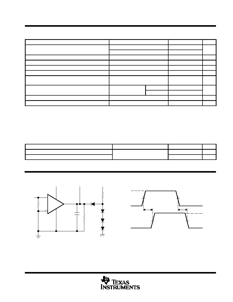
PARAMETER MEASUREMENT INFORMATION
VCC +
Output
VCC +
392
3.92 k
CL = 30 pF
(see Note A)
Input
51
TEST CIRCUIT
VOLTAGE WAVEFORMS
0.5 V
Input
50%
50%
(see Note B)
0.5 V
tPHL
tPLH
VOH
VOL
1.5 V
1.5 V
Output
NOTES: A. CL includes probe and jig capacitance.
B. The input pulse is supplied by a generator having the following characteristics: tr
5 ns, tf
5 ns, PRR
300 kHz,
duty cycle = 50%.
Figure 1. Test Circuit and Voltage Waveforms
SN75146
DUAL DIFFERENTIAL LINE RECEIVER
SLLS015B FEBRUARY 1986 REVISED MAY 1995
4
POST OFFICE BOX 655303
·
DALLAS, TEXAS 75265
TYPICAL CHARACTERISTICS
Figure 2
100
VO Output V
oltage V
VID Differential Input Voltage mV
4
100
0
50
0
50
1
2
3
VCC = 4.75 V
VIC = 0
VIC =
±
7 V
VIC = 0
VIC =
±
7 V
OUTPUT VOLTAGE
vs
DIFFERENTIAL INPUT VOLTAGE
ÁÁ
ÁÁ
V
O
ÏÏÏÏ
ÏÏÏÏ
TA = 25
°
C
100
VID Differential Input Voltage mV
4
100
0
50
0
50
1
2
3
VCC = 5.25 V
VIC = 0
VIC =
±
7 V
VIC = 0
VIC =
±
7 V
OUTPUT VOLTAGE
vs
DIFFERENTIAL INPUT VOLTAGE
VO Output V
oltage V
ÁÁ
ÁÁ
V
O
ÏÏÏÏÏ
ÏÏÏÏÏ
TA = 25
°
C
Figure 3
SN75146
DUAL DIFFERENTIAL LINE RECEIVER
SLLS015B FEBRUARY 1986 REVISED MAY 1995
5
POST OFFICE BOX 655303
·
DALLAS, TEXAS 75265
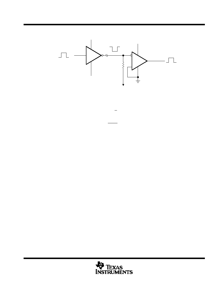
APPLICATION INFORMATION
12 V
1/2 uA9636
12 V
See Note A
V
R
1/2 SN75146
5 V
NOTE A: In order to meet the input-impedance and open-circuit-input voltage requirements of
ANSI Standard EIA/TIA-232-E and ITU recommendation V.28 and ensure
open-circuit-input fail-safe operation, R and V are selected to satisfy the following
equations:
V
+
1.13.3 R
r
i
volts
3 k
W v
R r
i
R
)
r
i
v
7 k
W
Figure 4. EIA/TIA-232-E System Applications