SN74TVC3306
DUAL VOLTAGE CLAMP
SCDS112C MARCH 2001 REVISED MARCH 2002
1
POST OFFICE BOX 655303
·
DALLAS, TEXAS 75265
D
Designed to Be Used in Voltage-Limiting
Applications
D
3.5-
On-State Connection Between Ports
A and B
D
Flow-Through Pinout for Ease of Printed
Circuit Board Trace Routing
D
Direct Interface With GTL+ Levels
D
Latch-Up Performance Exceeds 100 mA Per
JESD 78, Class II
D
ESD Protection Exceeds JESD 22
2000-V Human-Body Model (A114-A)
200-V Machine Model (A115-A)
1000-V Charged-Device Model (C101)
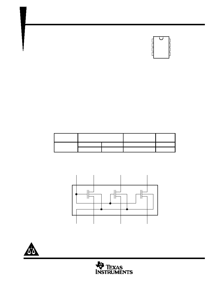
description
The SN74TVC3306 provides three parallel NMOS pass transistors with a common unbuffered gate. The low
on-state resistance of the switch allows connections to be made with minimal propagation delay.
The device can be used as a dual switch, with the gates cascaded together to a reference transistor. The
low-voltage side of each pass transistor is limited to a voltage set by the reference transistor. This is done to
protect components with inputs that are sensitive to high-state voltage-level overshoots.
ORDERING INFORMATION
TA
PACKAGE
ORDERABLE
PART NUMBER
TOP-SIDE
MARKING
40
°
C to 85
°
C
SSOP DCT
Tape and reel
SN74TVC3306DCTR
FA6
40
°
C to 85
°
C
VSSOP DCU
Tape and reel
SN74TVC3306DCUR
FA6
Package drawings, standard packing quantities, thermal data, symbolization, and PCB design
guidelines are available at www.ti.com/sc/package.
logic diagram (positive logic)
B2
B3
A2
A3
A1
GND
B1
GATE
NOTE A: The SN74TVC3306 has bidirectional capability across many voltage levels. The voltage levels documented in this data sheet are
examples.
8
7
6
5
1
2
3
4
Copyright
2002, Texas Instruments Incorporated
Please be aware that an important notice concerning availability, standard warranty, and use in critical applications of
Texas Instruments semiconductor products and disclaimers thereto appears at the end of this data sheet.
DCT OR DCU PACKAGE
(TOP VIEW)
1
2
3
4
8
7
6
5
GND
A1
A2
A3
GATE
B1
B2
B3
PRODUCTION DATA information is current as of publication date.
Products conform to specifications per the terms of Texas Instruments
standard warranty. Production processing does not necessarily include
testing of all parameters.

SN74TVC3306
DUAL VOLTAGE CLAMP
SCDS112C MARCH 2001 REVISED MARCH 2002
2
POST OFFICE BOX 655303
·
DALLAS, TEXAS 75265
absolute maximum ratings over operating free-air temperature range (unless otherwise noted)
Input voltage range, V
I
(see Note 1)
0.5 V to 7 V
. . . . . . . . . . . . . . . . . . . . . . . . . . . . . . . . . . . . . . . . . . . . . . . . . .
Input/output voltage range, V
I/O
(see Note 1)
0.5 V to 7 V
. . . . . . . . . . . . . . . . . . . . . . . . . . . . . . . . . . . . . . . . . .
Continuous channel current
128 mA
. . . . . . . . . . . . . . . . . . . . . . . . . . . . . . . . . . . . . . . . . . . . . . . . . . . . . . . . . . . . . .
Input clamp current, I
IK
(V
I
< 0)
50 mA
. . . . . . . . . . . . . . . . . . . . . . . . . . . . . . . . . . . . . . . . . . . . . . . . . . . . . . . . . . .
Package thermal impedance,
JA
(see Note 2): DCT package
220
°
C/W
. . . . . . . . . . . . . . . . . . . . . . . . . . . . . . .
DCU package
227
°
C/W
. . . . . . . . . . . . . . . . . . . . . . . . . . . . . . .
Storage temperature range, T
stg
65
°
C to 150
°
C
. . . . . . . . . . . . . . . . . . . . . . . . . . . . . . . . . . . . . . . . . . . . . . . . . . .
Stresses beyond those listed under "absolute maximum ratings" may cause permanent damage to the device. These are stress ratings only, and
functional operation of the device at these or any other conditions beyond those indicated under "recommended operating conditions" is not
implied. Exposure to absolute-maximum-rated conditions for extended periods may affect device reliability.
NOTES:
1. The input and input/output negative-voltage ratings may be exceeded if the input and input/output clamp-current ratings are
observed.
2. The package thermal impedance is calculated in accordance with JESD 51-7.
recommended operating conditions
MIN
MAX
UNIT
VI/O
Input/output voltage
0
5
V
VGATE
GATE voltage
0
5
V
IPASS
Pass transistor current
64
mA
TA
Operating free-air temperature
40
85
°
C
electrical characteristics over recommended operating free-air temperature range (unless
otherwise noted)
PARAMETER
TEST CONDITIONS
MIN
TYP
MAX
UNIT
VIK
II = 18 mA,
VGATE = 0
1.2
V
IIH
VI = 5 V,
VGATE = 0
5
µ
A
Ci(GATE)
VI = 3 V or 0
11
pF
Cio(off)
VO = 3 V or 0,
VGATE = 0
4
6
pF
Cio(on)
VO = 3 V or 0,
VGATE = 3 V
10.5
12.5
pF
§
VGATE = 4.5 V
3.5
5.5
§
VI = 0
IO = 64 mA
VGATE = 3 V
4.7
7
§
VI = 0
IO = 64 mA
VGATE = 2.3 V
6.3
9.5
ron§
VGATE = 1.5 V
25.5
32
VI = 2 4 V
VGATE = 4.5 V
4.8
7.5
VI = 2.4 V
IO = 15 mA
VGATE = 3 V
14.7
23
VI = 1.7 V
VGATE = 2.3 V
11.3
16.5
All typical values are at TA = 25
°
C.
§ Measured by the voltage drop between the A and B terminals at the indicated current through the switch. On-state resistance is determined by
the lowest voltage of the two (A or B) terminals.
SN74TVC3306
DUAL VOLTAGE CLAMP
SCDS112C MARCH 2001 REVISED MARCH 2002
3
POST OFFICE BOX 655303
·
DALLAS, TEXAS 75265
ac performance (translating down)
switching characteristics over recommended operating free-air temperature range, V
GATE
= 3.3 V,
V
IH
= 3.3 V, V
IL
= 0, and V
M
= 1.15 V (unless otherwise noted) (see Figure 1)
PARAMETER
FROM
TO
CL = 50 pF
CL = 30 pF
CL = 15 pF
UNIT
PARAMETER
(INPUT)
(OUTPUT)
MIN
MAX
MIN
MAX
MIN
MAX
UNIT
tPLH
A or B
B or A
0
0.8
0
0.6
0
0.3
ns
tPHL
A or B
B or A
0
1.2
0
1
0
0.5
ns
switching characteristics over recommended operating free-air temperature range, V
GATE
= 2.5 V,
V
IH
= 2.5 V, V
IL
= 0, and V
M
= 0.75 V (unless otherwise noted) (see Figure 1)
PARAMETER
FROM
TO
CL = 50 pF
CL = 30 pF
CL = 15 pF
UNIT
PARAMETER
(INPUT)
(OUTPUT)
MIN
MAX
MIN
MAX
MIN
MAX
UNIT
tPLH
A or B
B or A
0
1
0
0.7
0
0.4
ns
tPHL
A or B
B or A
0
1.3
0
1
0
0.6
ns
ac performance (translating up)
switching characteristics over recommended operating free-air temperature range, V
GATE
= 3.3 V,
V
IH
= 2.3 V, V
IL
= 0, V
T
= 3.3 V, V
M
= 1.15 V, and R
L
= 300
(unless otherwise noted) (see Figure 1)
PARAMETER
FROM
TO
CL = 50 pF
CL = 30 pF
CL = 15 pF
UNIT
PARAMETER
(INPUT)
(OUTPUT)
MIN
MAX
MIN
MAX
MIN
MAX
UNIT
tPLH
A or B
B or A
0
0.9
0
0.6
0
0.4
ns
tPHL
A or B
B or A
0
1.4
0
1.1
0
0.7
ns
switching characteristics over recommended operating free-air temperature range, V
GATE
= 2.5 V,
V
IH
= 1.5 V, V
IL
= 0, V
T
= 2.5 V, V
M
= 0.75 V, and R
L
= 300
(unless otherwise noted) (see Figure 1)
PARAMETER
FROM
TO
CL = 50 pF
CL = 30 pF
CL = 15 pF
UNIT
PARAMETER
(INPUT)
(OUTPUT)
MIN
MAX
MIN
MAX
MIN
MAX
UNIT
tPLH
A or B
B or A
0
1
0
0.6
0
0.4
ns
tPHL
A or B
B or A
0
1.3
0
1.3
0
0.8
ns

SN74TVC3306
DUAL VOLTAGE CLAMP
SCDS112C MARCH 2001 REVISED MARCH 2002
4
POST OFFICE BOX 655303
·
DALLAS, TEXAS 75265
PARAMETER MEASUREMENT INFORMATION
NOTES: A. CL includes probe and jig capacitance.
B. All input pulses are supplied by generators having the following characteristics: PRR
10 MHz, ZO = 50
, tr
2 ns, tf
2 ns.
C. The outputs are measured one at a time with one transition per measurement.
From Output
Under Test
CL
(see Note A)
LOAD CIRCUIT
RL
Translating up
Translating down
S1
S2
USAGE
SWITCH
VM
VM
VIH
VIL
Input
VM
VM
VOH
VOL
Output
VT
S1
S2
Open
Figure 1. Load Circuit for Outputs
SN74TVC3306
DUAL VOLTAGE CLAMP
SCDS112C MARCH 2001 REVISED MARCH 2002
5
POST OFFICE BOX 655303
·
DALLAS, TEXAS 75265
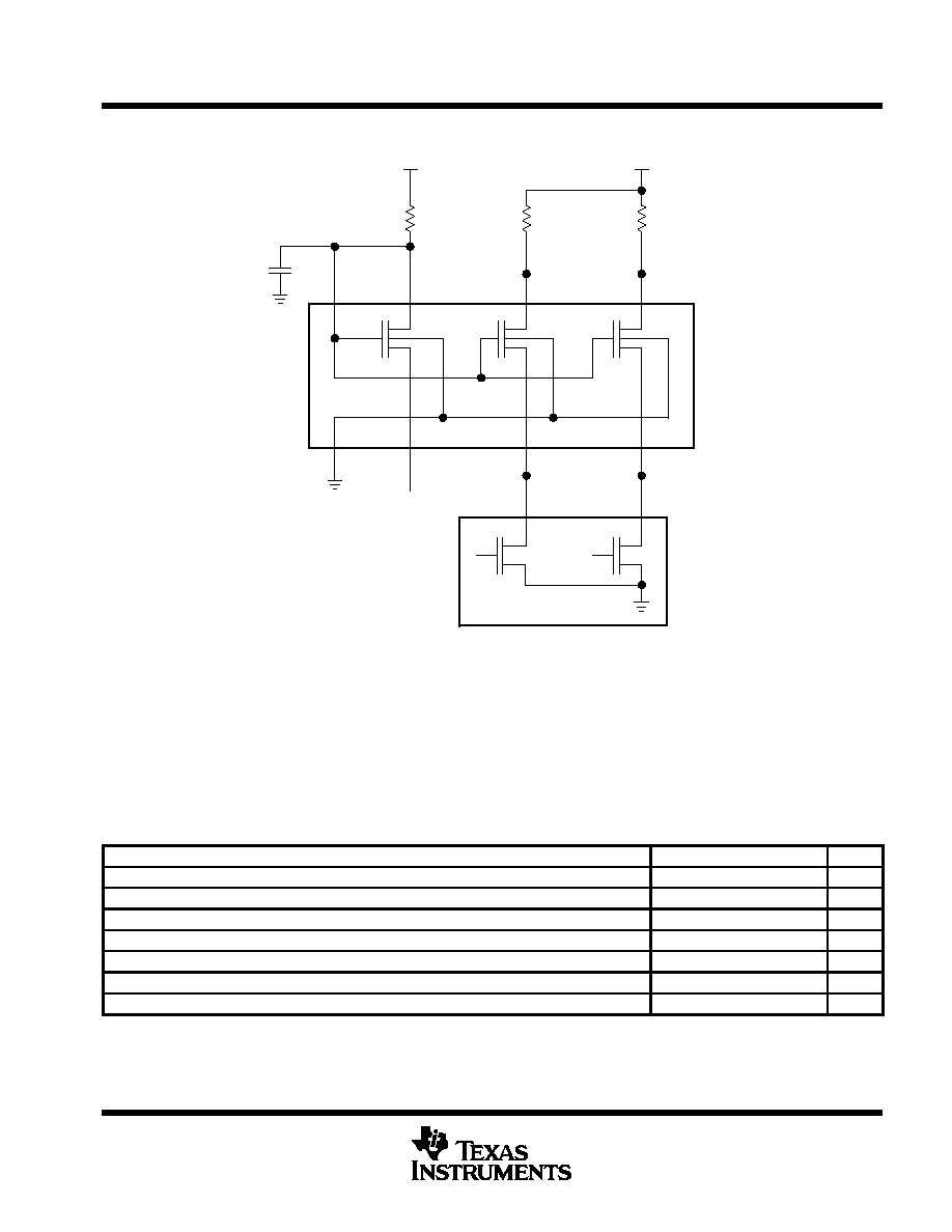
APPLICATION INFORMATION
150
Open-Drain
CPU Interface
Motherboard
Interface
VREF = 1.5 V
GATE
B1 (VBIAS)
TVC3306
VREF and VBIAS can be applied to any one of the pass transistors. GATE must be connected externally to VBIAS.
B3
8
7
6
5
1
2
3
4
150
200 k
B2
VDDREF = 3.3 V
VDPU = 2.5 V
A3
A2
A1
Figure 2. Typical Application Circuit
For the clamping configuration, the common GATE input must be connected to one side (An or Bn) of any one of the
pass transistors, making that the V
BIAS
connection of the reference transistor and the opposite side (Bn or An) the
V
REF
connection. When V
BIAS
is connected through a 200-k
resistor to a 3-V to 5.5-V V
CC
supply and V
REF
is set
to 0 V to V
CC
0.6 V, the output of each switch has a maximum clamp voltage equal to V
REF
. A filter capacitor on
V
BIAS
is recommended.
application operating conditions (see Figure 2)
MIN
TYP
MAX
UNIT
VBIAS
BIAS voltage
VREF + 0.6
2.1
5
V
VGATE
GATE voltage
VREF + 0.6
2.1
5
V
VREF
Reference voltage
0
1.5
4.4
V
VDPU
Drain pullup voltage
2.36
2.5
2.64
V
IPASS
Pass-transistor current
14
mA
IREF
Reference-transistor current
5
µ
A
TA
Operating free-air temperature
40
85
°
C
All typical values are at TA = 25
°
C.