SN54LVTH18502A, SN54LVTH182502A, SN74LVTH18502A, SN74LVTH182502A
3.3 V ABT SCAN TEST DEVICES
WITH 18 BIT UNIVERSAL BUS TRANSCEIVERS
SCBS668C - JULY 1996 - REVISED JUNE 2004
1
POST OFFICE BOX 655303
·
DALLAS, TEXAS 75265
D
Members of the Texas Instruments
SCOPE
Family of Testability Products
D
Members of the Texas Instruments
Widebus
Family
D
State-of-the-Art 3.3-V ABT Design Supports
Mixed-Mode Signal Operation (5-V Input
and Output Voltages With 3.3-V V
CC
)
D
Support Unregulated Battery Operation
Down to 2.7 V
D
UBT
(Universal Bus Transceiver)
Combines D-Type Latches and D-Type
Flip-Flops for Operation in Transparent,
Latched, or Clocked Mode
D
Bus Hold on Data Inputs Eliminates the
Need for External Pullup Resistors
D
B-Port Outputs of 'LVTH182502A Devices
Have Equivalent 25-
Series Resistors, So
No External Resistors Are Required
D
Compatible With the IEEE Standard
1149.1-1990 (JTAG) Test Access Port and
Boundary-Scan Architecture
D
SCOPE
Instruction Set
- IEEE Standard 1149.1-1990 Required
Instructions and Optional CLAMP and
HIGHZ
- Parallel-Signature Analysis at Inputs
- Pseudorandom Pattern Generation From
Outputs
- Sample Inputs/Toggle Outputs
- Binary Count From Outputs
- Device Identification
- Even-Parity Opcodes
D
Packaged in 64-Pin Plastic Thin Quad Flat
(PM) Packages Using 0.5-mm
Center-to-Center Spacings and 68-Pin
Ceramic Quad Flat (HV) Packages Using
25-mil Center-to-Center Spacings
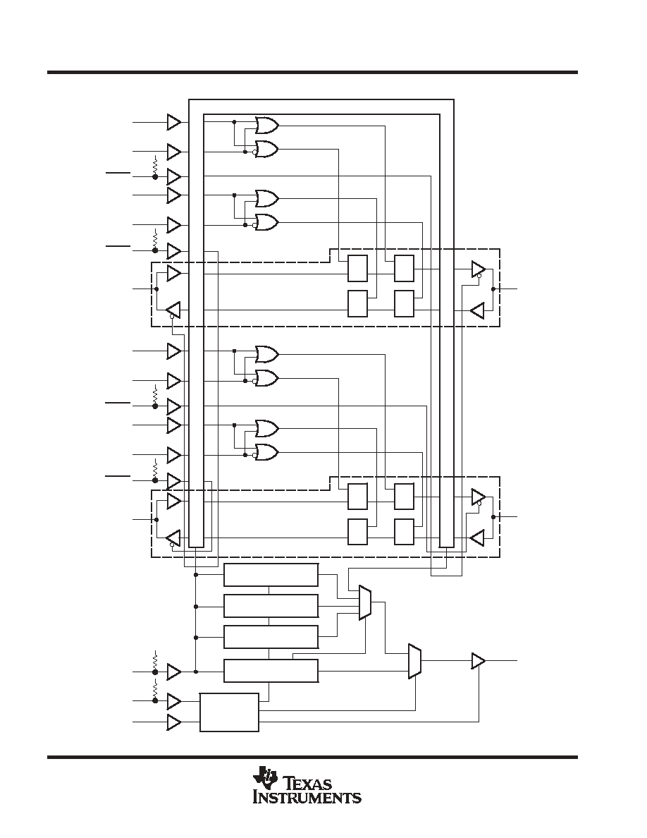
description
The 'LVTH18502A and 'LVTH182502A scan test devices with 18-bit universal bus transceivers are members
of the Texas Instruments SCOPE
testability integrated-circuit family. This family of devices supports IEEE
Standard 1149.1-1990 boundary scan to facilitate testing of complex circuit-board assemblies. Scan access to
the test circuitry is accomplished via the 4-wire test access port (TAP) interface.
Additionally, these devices are designed specifically for low-voltage (3.3-V) V
CC
operation, but with the
capability to provide a TTL interface to a 5-V system environment.
In the normal mode, these devices are 18-bit universal bus transceivers, that combine with D-type latches and
D-type flip-flops, they allow data to flow in the transparent, latched, or clocked modes. Another use is as two
9-bit transceivers or one 18-bit transceiver. The test circuitry can be activated by the TAP to take snapshot
samples of the data appearing at the device pins or to perform a self test on the boundary-test cells. Activating
the TAP in the normal mode does not affect the functional operation of the SCOPE universal bus transceivers.
Data flow in each direction is controlled by output-enable (OEAB and OEBA), latch-enable (LEAB and LEBA),
and clock (CLKAB and CLKBA) inputs. For A-to-B data flow, the device operates in the transparent mode when
LEAB is high. When LEAB is low, the A-bus data is latched while CLKAB is held at a static low or high logic level.
Otherwise, if LEAB is low, A-bus data is stored on a low-to-high transition of CLKAB. When OEAB is low, the
B outputs are active. When OEAB is high, the B outputs are in the high-impedance state. B-to-A data flow is
similar to A-to-B data flow, but uses the OEBA, LEBA, and CLKBA inputs.
In the test mode, the normal operation of the SCOPE universal bus transceivers is inhibited, and the test circuitry
is enabled to observe and control the I/O boundary of the device. When enabled, the test circuitry performs
boundary-scan test operations according to the protocol described in IEEE Standard 1149.1-1990.
Copyright
2004, Texas Instruments Incorporated
UNLESS OTHERWISE NOTED this document contains PRODUCTION
DATA information current as of publication date. Products conform to
specifications per the terms of Texas Instruments standard warranty.
Production processing does not necessarily include testing of all
parameters.
SCOPE, Widebus, and UBT are trademarks of Texas Instruments.
Please be aware that an important notice concerning availability, standard warranty, and use in critical applications of
Texas Instruments semiconductor products and disclaimers thereto appears at the end of this data sheet.
SN54LVTH18502A, SN54LVTH182502A, SN74LVTH18502A, SN74LVTH182502A
3.3 V ABT SCAN TEST DEVICES
WITH 18 BIT UNIVERSAL BUS TRANSCEIVERS
SCBS668C - JULY 1996 - REVISED JUNE 2004
2
POST OFFICE BOX 655303
·
DALLAS, TEXAS 75265
description (continued)
Four dedicated test pins are used to observe and control the operation of the test circuitry: test data input (TDI),
test data output (TDO), test mode select (TMS), and test clock (TCK). Additionally, the test circuitry performs
other testing functions such as parallel-signature analysis (PSA) on data inputs and pseudorandom pattern
generation (PRPG) from data outputs. All testing and scan operations are synchronized to the TAP interface.
Active bus-hold circuitry is provided to hold unused or floating data inputs at a valid logic level.
The B-port outputs of 'LVTH182502A, which are designed to source or sink up to 12 mA, include 25-
series
resistors to reduce overshoot and undershoot.
The SN54LVTH18502A and SN54LVTH182502A are characterized for operation over the full military
temperature range of -55
°
C to 125
°
C. The SN74LVTH18502A and SN74LVTH182502A are characterized for
operation from -40
°
C to 85
°
C.
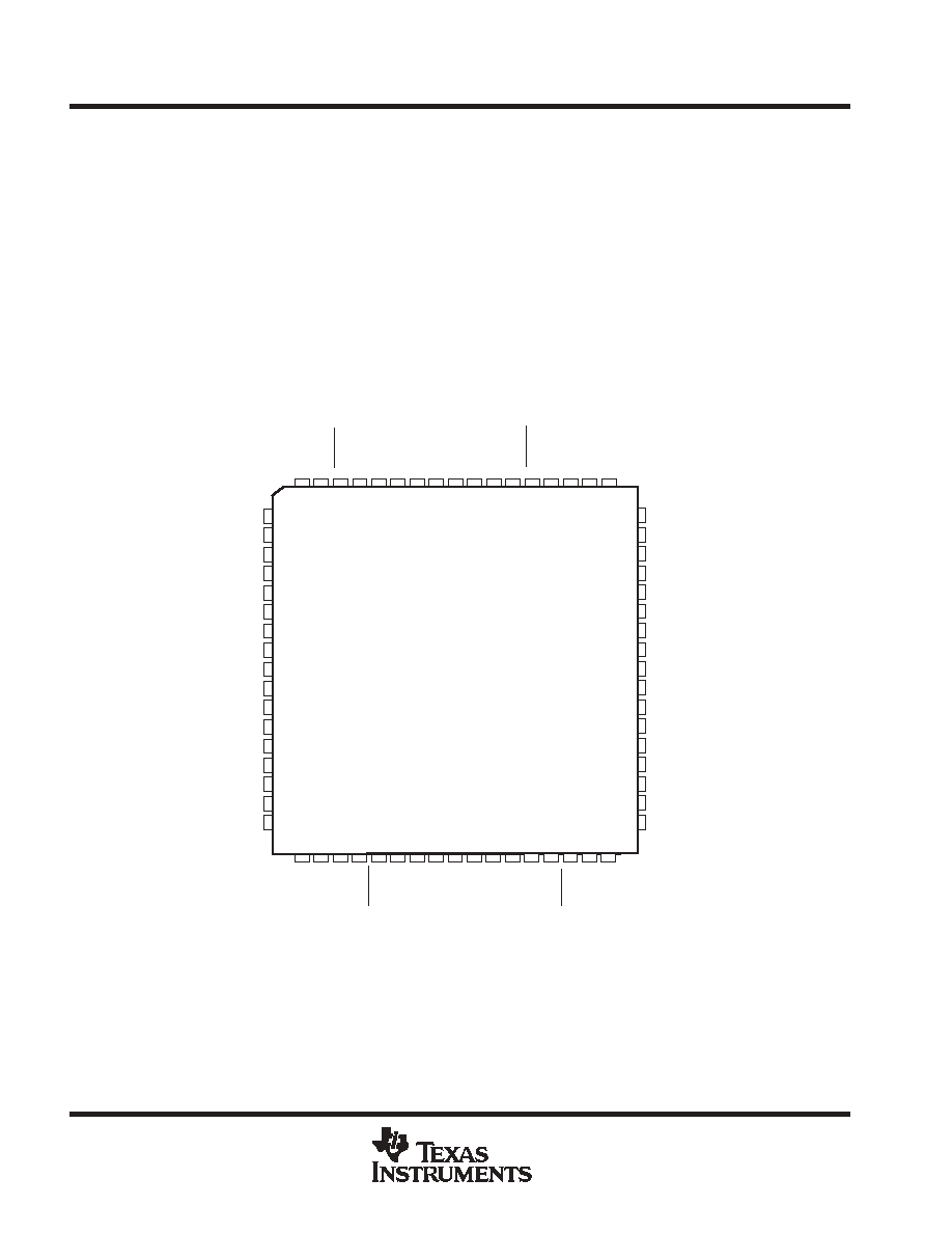
1B4
1B5
1B6
GND
1B7
1B8
1B9
V
CC
NC
2B1
2B2
2B3
2B4
GND
2B5
2B6
2B7
1A3
1A4
1A5
GND
1A6
1A7
1A8
1A9
NC
V
CC
2A1
2A2
2A3
GND
2A4
2A5
2A6
V
NC
TMS
1CLKBA
1A2
1A1
1OEAB
GND
1LEAB
1CLKAB
TDO
NC
TCK
2CLKBA
2LEBA
2A9
GND
2OEAB
2LEAB
2CLKAB
TDI
2A7
2A8
1LEBA
1O
1OEBA
GND
2OEBA
2B9
2B8
GND
1B1
1B2
1B3
SN54LVTH18502A, SN54LVTH182502A . . . HV PACKAGE
(TOP VIEW)
CC
V
CC
NC - No internal connection
60
59
58
57
56
55
54
53
52
51
50
49
48
47
46
45
44
10
11
12
13
14
15
16
17
18
19
20
21
22
23
24
25
26
28 29 30 31 32 33 34
8
7
6
5
4
9
3
1 68 67
2
35 36 37 38 39
66 65
27
64 63 62 61
40 41 42 43
SN54LVTH18502A, SN54LVTH182502A, SN74LVTH18502A, SN74LVTH182502A
3.3 V ABT SCAN TEST DEVICES
WITH 18 BIT UNIVERSAL BUS TRANSCEIVERS
SCBS668C - JULY 1996 - REVISED JUNE 2004
3
POST OFFICE BOX 655303
·
DALLAS, TEXAS 75265
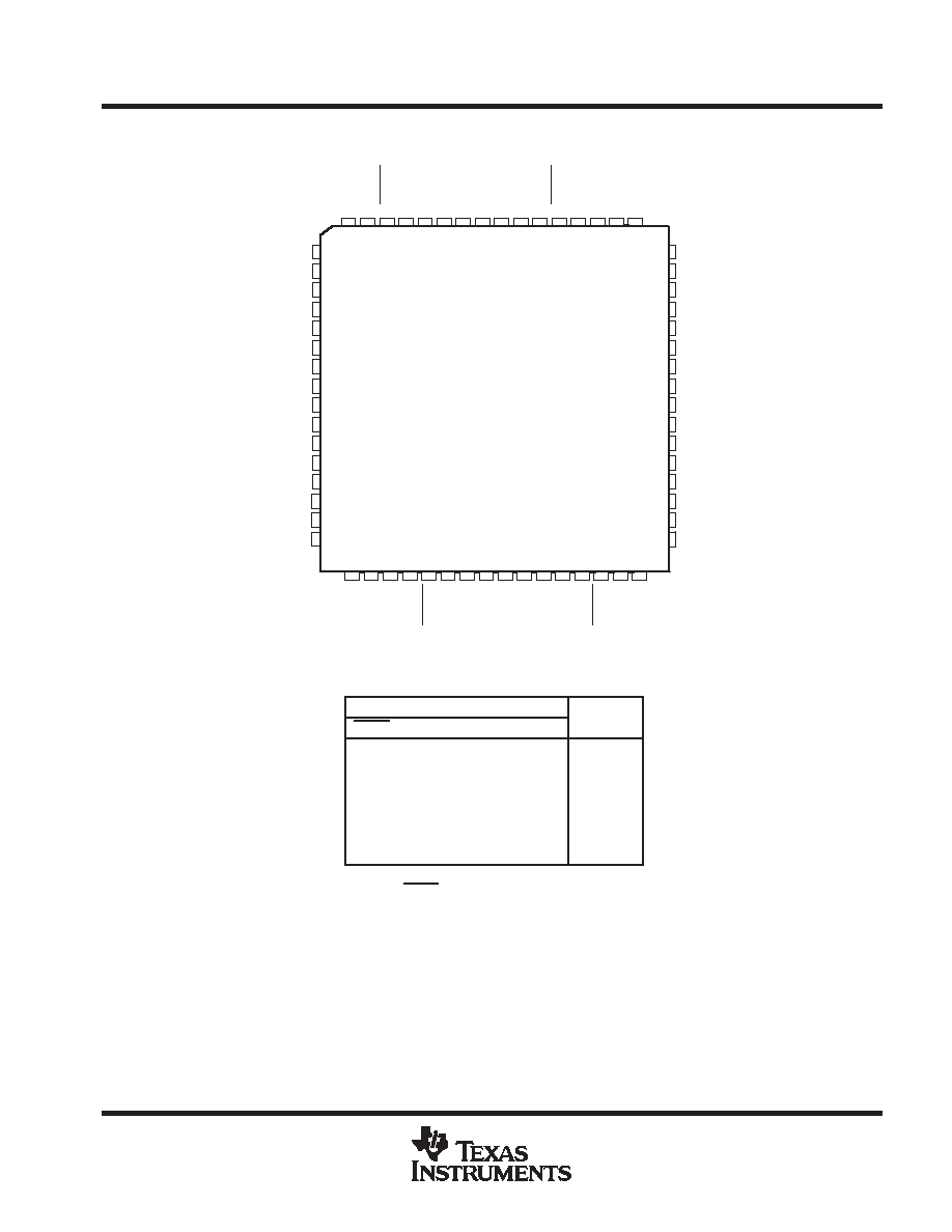
1B4
1B5
1B6
GND
1B7
1B8
1B9
V
CC
2B1
2B2
2B3
2B4
GND
2B5
2B6
2B7
18 19
48
47
46
45
44
43
42
41
40
39
38
37
36
35
34
33
20
1
2
3
4
5
6
7
8
9
10
11
12
13
14
15
16
21 22 23 24
63 62 61 60 59
64
58
56 55 54
57
25 26 27 28 29
53 52
17
51 50 49
30 31 32
1OEAB
GND
1CLKAB
TDO
1A2
1A1
1LEAB
V
1LEBA
1OEBA
1B1
1B2
TMS
1CLKBA
GND
1B3
2A9
GND
2LEAB
2CLKAB
2A7
2A8
2OEAB
TDI
2CLKBA
2LEBA
2OEBA
2B9
V
TCK
GND
2B8
1A3
1A4
1A5
GND
1A6
1A7
1A8
1A9
V
CC
2A1
2A2
2A3
GND
2A4
2A5
2A6
CC
CC
SN74LVTH18502A, SN74LVTH182502A . . . PM PACKAGE
(TOP VIEW)
FUNCTION TABLE
(normal mode, each register)
INPUTS
OUTPUT
OEAB
LEAB
CLKAB
A
OUTPUT
B
L
L
L
X
B0
L
L
L
L
L
L
H
H
L
H
X
L
L
L
H
X
H
H
H
X
X
X
Z
A-to-B data flow is shown. B-to-A data flow is similar,
but uses OEBA, LEBA, and CLKBA.
Output level before the indicated steady-state input
conditions are established
SN54LVTH18502A, SN54LVTH182502A, SN74LVTH18502A, SN74LVTH182502A
3.3 V ABT SCAN TEST DEVICES
WITH 18 BIT UNIVERSAL BUS TRANSCEIVERS
SCBS668C - JULY 1996 - REVISED JUNE 2004
5
POST OFFICE BOX 655303
·
DALLAS, TEXAS 75265
Terminal Functions
TERMINAL NAME
DESCRIPTION
1A1-1A9,
2A1-2A9
Normal-function A-bus I/O ports. See function table for normal-mode logic.
1B1-1B9,
2B1-2B9
Normal-function B-bus I/O ports. See function table for normal-mode logic.
1CLKAB, 1CLKBA,
2CLKAB, 2CLKBA
Normal-function clock inputs. See function table for normal-mode logic.
GND
Ground
1LEAB, 1LEBA,
2LEAB, 2LEBA
Normal-function latch enables. See function table for normal-mode logic.
1OEAB, 1OEBA,
2OEAB, 2OEBA
Normal-function output enables. See function table for normal-mode logic. An internal pullup at each terminal forces the
terminal to a high level if left unconnected.
TCK
Test clock. One of four terminals required by IEEE Standard 1149.1-1990. Test operations of the device are synchronous
to TCK. Data is captured on the rising edge of TCK and outputs change on the falling edge of TCK.
TDI
Test data input. One of four terminals required by IEEE Standard 1149.1-1990. TDI is the serial input for shifting data
through the instruction register or selected data register. An internal pullup forces TDI to a high level if left unconnected.
TDO
Test data output. One of four terminals required by IEEE Standard 1149.1-1990. TDO is the serial output for shifting data
through the instruction register or selected data register.
TMS
Test mode select. One of four terminals required by IEEE Standard 1149.1-1990. TMS directs the device through its TAP
controller states. An internal pullup forces TMS to a high level if left unconnected.
VCC
Supply voltage