
SN54HCT138, SN74HCT138
3-LINE TO 8-LINE DECODERS/DEMULTIPLEXERS
SCLS171C MARCH 1984 REVISED MAY 1997
1
POST OFFICE BOX 655303
·
DALLAS, TEXAS 75265
D
Inputs Are TTL-Voltage Compatible
D
Designed Specifically for High-Speed
Memory Decoders and Data Transmission
Systems
D
Incorporate Three Enable Inputs to Simplify
Cascading and/or Data Reception
D
Package Options Include Plastic
Small-Outline (D), Thin Shrink
Small-Outline (PW), and Ceramic Flat (W)
Packages, Ceramic Chip Carriers (FK), and
Standard Plastic (N) and Ceramic (J)
300-mil DIPs
description
The 'HCT138 are designed for high-performance
memory-decoding or data-routing applications
requiring very short propagation delay times. In
high-performance memory systems, these
decoders can minimize the effects of system
decoding. When employed with high-speed
memories utilizing a fast enable circuit, the delay
times of these decoders and the enable time of the
memory are usually less than the typical access
time of the memory. This means that the effective
system delay introduced by the decoders is
negligible.
The conditions at the binary-select inputs and the three enable inputs select one of eight output lines. Two
active-low (G) and one active-high (G) enable inputs reduce the need for external gates or inverters when
expanding. A 24-line decoder can be implemented without external inverters and a 32-line decoder requires
only one inverter. An enable input can be used as a data input for demultiplexing applications.
The SN54HCT138 is characterized for operation over the full military temperature range of 55
°
C to 125
°
C. The
SN74HCT138 is characterized for operation from 40
°
C to 85
°
C.
3
2 1 20 19
9 10 11 12 13
4
5
6
7
8
18
17
16
15
14
Y1
Y2
NC
Y3
Y4
C
G2A
NC
G2B
G1
B
A
NC
Y6
Y5
V
Y0
Y7
GND
NC
SN54HCT138 . . . FK PACKAGE
(TOP VIEW)
CC
NC No internal connection
1
2
3
4
5
6
7
8
16
15
14
13
12
11
10
9
A
B
C
G2A
G2B
G1
Y7
GND
V
CC
Y0
Y1
Y2
Y3
Y4
Y5
Y6
SN54HCT138 . . . J OR W PACKAGE
SN74HCT138 . . . D, N, OR PW PACKAGE
(TOP VIEW)
Copyright
©
1997, Texas Instruments Incorporated
Please be aware that an important notice concerning availability, standard warranty, and use in critical applications of
Texas Instruments semiconductor products and disclaimers thereto appears at the end of this data sheet.
PRODUCTION DATA information is current as of publication date.
Products conform to specifications per the terms of Texas Instruments
standard warranty. Production processing does not necessarily include
testing of all parameters.

SN54HCT138, SN74HCT138
3-LINE TO 8-LINE DECODERS/DEMULTIPLEXERS
SCLS171C MARCH 1984 REVISED MAY 1997
2
POST OFFICE BOX 655303
·
DALLAS, TEXAS 75265
FUNCTION TABLE
INPUTS
OUTPUTS
ENABLE
SELECT
OUTPUTS
G1
G2A
G2B
C
B
A
Y0
Y1
Y2
Y3
Y4
Y5
Y6
Y7
X
H
X
X
X
X
H
H
H
H
H
H
H
H
X
X
H
X
X
X
H
H
H
H
H
H
H
H
L
X
X
X
X
X
H
H
H
H
H
H
H
H
H
L
L
L
L
L
L
H
H
H
H
H
H
H
H
L
L
L
L
H
H
L
H
H
H
H
H
H
H
L
L
L
H
L
H
H
L
H
H
H
H
H
H
L
L
L
H
H
H
H
H
L
H
H
H
H
H
L
L
H
L
L
H
H
H
H
L
H
H
H
H
L
L
H
L
H
H
H
H
H
H
L
H
H
H
L
L
H
H
L
H
H
H
H
H
H
L
H
H
L
L
H
H
H
H
H
H
H
H
H
H
L
logic symbols (alternatives)
1
1
A
Y0
15
0
2
2
B
4
3
C
Y1
14
1
Y2
13
2
Y3
12
3
Y4
11
4
Y5
10
5
Y6
9
6
Y7
7
7
BIN/OCT
6
4
5
G1
G2A
G2B
&
EN
0
1
A
Y0
15
0
2
B
2
3
C
Y1
14
1
Y2
13
2
Y3
12
3
Y4
11
4
Y5
10
5
Y6
9
6
Y7
7
7
DMUX
6
4
5
G1
G2A
G2B
&
G
0
7
These symbols are in accordance with ANSI/IEEE Std 91-1984 and IEC Publication 617-12.
Pin numbers shown are for the D, J, N, PW, and W packages.

SN54HCT138, SN74HCT138
3-LINE TO 8-LINE DECODERS/DEMULTIPLEXERS
SCLS171C MARCH 1984 REVISED MAY 1997
3
POST OFFICE BOX 655303
·
DALLAS, TEXAS 75265
logic diagram (positive logic)
A
Y0
Y1
Y2
Y3
Y4
Y5
Y6
Y7
B
C
G1
G2A
G2B
Pin numbers shown are for the D, J, N, PW, and W packages.
1
2
3
6
4
5
15
14
13
12
11
10
9
7
absolute maximum ratings over operating free-air temperature range
Supply voltage range, V
CC
0.5 V to 7 V
. . . . . . . . . . . . . . . . . . . . . . . . . . . . . . . . . . . . . . . . . . . . . . . . . . . . . . . . . .
Input clamp current, I
IK
(V
I
< 0 or V
I
> V
CC
) (see Note 1)
±
20 mA
. . . . . . . . . . . . . . . . . . . . . . . . . . . . . . . . . . . .
Output clamp current, I
OK
(V
O
< 0 or V
O
> V
CC
) (see Note 1)
±
20 mA
. . . . . . . . . . . . . . . . . . . . . . . . . . . . . . . .
Continuous output current, I
O
(V
O
= 0 to V
CC
)
±
25 mA
. . . . . . . . . . . . . . . . . . . . . . . . . . . . . . . . . . . . . . . . . . . . . .
Continuous current through V
CC
or GND
±
50 mA
. . . . . . . . . . . . . . . . . . . . . . . . . . . . . . . . . . . . . . . . . . . . . . . . . . .
Package thermal impedance,
JA
(see Note 2): D package
113
°
C/W
. . . . . . . . . . . . . . . . . . . . . . . . . . . . . . . . . .
N package
78
°
C/W
. . . . . . . . . . . . . . . . . . . . . . . . . . . . . . . . . . .
Storage temperature range, T
stg
65
°
C to 150
°
C
. . . . . . . . . . . . . . . . . . . . . . . . . . . . . . . . . . . . . . . . . . . . . . . . . . .
Stresses beyond those listed under "absolute maximum ratings" may cause permanent damage to the device. These are stress ratings only, and
functional operation of the device at these or any other conditions beyond those indicated under "recommended operating conditions" is not
implied. Exposure to absolute-maximum-rated conditions for extended periods may affect device reliability.
NOTES:
1. The input and output voltage ratings may be exceeded if the input and output current ratings are observed.
2. The package thermal impedance is calculated in accordance with JESD 51, except for through-hole packages, which use a trace
length of zero.

SN54HCT138, SN74HCT138
3-LINE TO 8-LINE DECODERS/DEMULTIPLEXERS
SCLS171C MARCH 1984 REVISED MAY 1997
4
POST OFFICE BOX 655303
·
DALLAS, TEXAS 75265
recommended operating conditions
SN54HCT138
SN74HCT138
UNIT
MIN
NOM
MAX
MIN
NOM
MAX
UNIT
VCC
Supply voltage
4.5
5
5.5
4.5
5
5.5
V
VIH
High-level input voltage
VCC = 4.5 V to 5.5 V
2
2
V
VIL
Low-level input voltage
VCC = 4.5 V to 5.5 V
0
0.8
0
0.8
V
VI
Input voltage
0
VCC
0
VCC
V
VO
Output voltage
0
VCC
0
VCC
V
tt
Input transition (rise and fall) time
0
500
0
500
ns
TA
Operating free-air temperature
55
125
40
85
°
C
electrical characteristics over recommended operating free-air temperature range (unless
otherwise noted)
PARAMETER
TEST CONDITIONS
VCC
TA = 25
°
C
SN54HCT138
SN74HCT138
UNIT
PARAMETER
TEST CONDITIONS
VCC
MIN
TYP
MAX
MIN
MAX
MIN
MAX
UNIT
VOH
VI = VIH or VIL
IOH = 20
µ
A
4 5 V
4.4
4.499
4.4
4.4
V
VOH
VI = VIH or VIL
IOH = 4 mA
4.5 V
3.98
4.3
3.7
3.84
V
VOL
VI = VIH or VIL
IOL = 20
µ
A
4 5 V
0.001
0.1
0.1
0.1
V
VOL
VI = VIH or VIL
IOL = 4 mA
4.5 V
0.17
0.26
0.4
0.33
V
II
VI = VCC or 0
5.5 V
±
0.1
±
100
±
1000
±
1000
nA
ICC
VI = VCC or 0,
IO = 0
5.5 V
8
160
80
µ
A
ICC
One input at 0.5 V or 2.4 V,
Other inputs at 0 or VCC
5.5 V
1.4
2.4
3
2.9
mA
Ci
4.5 V
to 5.5 V
3
10
10
10
pF
This is the increase in supply current for each input that is at one of the specified TTL voltage levels rather than 0 V or VCC.
switching characteristics over recommended operating free-air temperature range, C
L
= 50 pF
(unless otherwise noted) (see Figure 1)
PARAMETER
FROM
TO
VCC
TA = 25
°
C
SN54HCT138
SN74HCT138
UNIT
PARAMETER
(INPUT)
(OUTPUT)
VCC
MIN
TYP
MAX
MIN
MAX
MIN
MAX
UNIT
A B or C
Any Y
4.5 V
23
36
54
45
t d
A, B, or C
Any Y
5.5 V
17
32
49
34
ns
tpd
Enable
Any Y
4.5 V
22
33
50
42
ns
Enable
Any Y
5.5 V
18
30
45
38
tt
Y
4.5 V
12
15
22
19
ns
tt
Y
5.5 V
11
14
20
17
ns
operating characteristics, T
A
= 25
°
C
PARAMETER
TEST CONDITIONS
TYP
UNIT
Cpd
Power dissipation capacitance
No load
85
pF
SN54HCT138, SN74HCT138
3-LINE TO 8-LINE DECODERS/DEMULTIPLEXERS
SCLS171C MARCH 1984 REVISED MAY 1997
5
POST OFFICE BOX 655303
·
DALLAS, TEXAS 75265
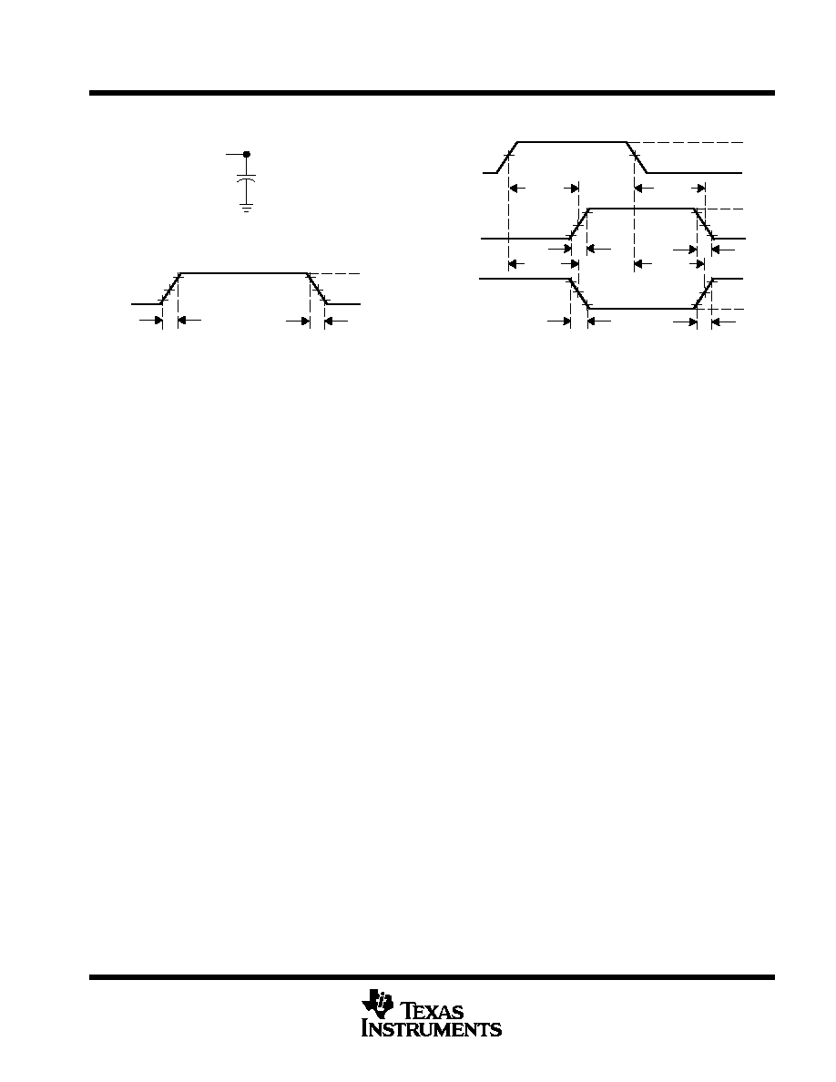
PARAMETER MEASUREMENT INFORMATION
VOLTAGE WAVEFORM
INPUT RISE AND FALL TIMES
1.3 V
1.3 V
0.3 V
0.3 V
2.7 V
2.7 V
3 V
0 V
tr
tf
Input
VOLTAGE WAVEFORMS
PROPAGATION DELAY AND OUTPUT RISE AND FALL TIMES
1.3 V
1.3 V
1.3 V
10%
10%
90%
90%
3 V
VOH
VOL
0 V
tr
tf
Input
In-Phase
Output
1.3 V
tPLH
tPHL
1.3 V
1.3 V
10%
10%
90%
90%
VOH
VOL
tr
tf
tPHL
tPLH
Out-of-Phase
Output
Test
Point
From Output
Under Test
LOAD CIRCUIT
NOTES: A. CL includes probe and test-fixture capacitance.
B. Phase relationships between waveforms were chosen arbitrarily. All input pulses are supplied by generators having the following
characteristics: PRR
1 MHz, ZO = 50
, tr = 6 ns, tf = 6 ns.
C. The outputs are measured one at a time with one input transition per measurement.
D. tPLH and tPHL are the same as tpd.
CL = 50 pF
(see Note A)
Figure 1. Load Circuit and Voltage Waveforms