Äîêóìåíòàöèÿ è îïèñàíèÿ www.docs.chipfind.ru
SN54AS194, SN74AS194
4-BIT BIDIRECTIONAL UNIVERSAL SHIFT REGISTERS
SDAS212A DECEMBER 1983 REVISED DECEMBER 1994
Copyright
©
1994, Texas Instruments Incorporated
1
POST OFFICE BOX 655303
·
DALLAS, TEXAS 75265
·
Parallel-to-Serial, Serial-to-Parallel
Conversions
·
Left or Right Shifts
·
Parallel Synchronous Loading
·
Direct Overriding Clear
·
Temporary Data-Latching Capability
·
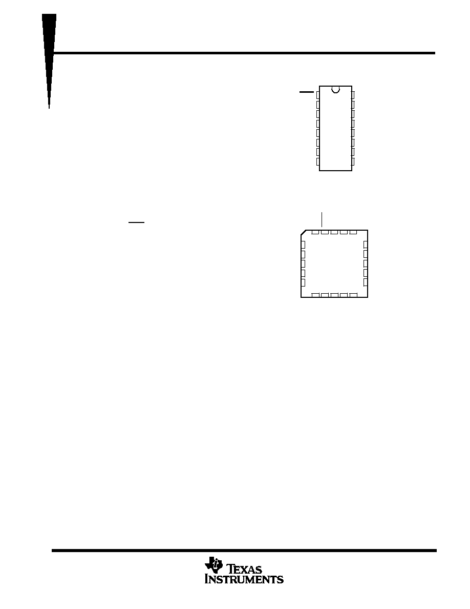
Package Options Include Plastic
Small-Outline Packages (D), Ceramic Chip
Carriers (FK), and Standard Plastic (N) and
Ceramic (J) 300-mil DIPs
description
These 4-bit bidirectional universal shift registers
feature parallel outputs, right-shift and left-shift
serial (SR SER, SL SER) inputs, operating-
mode-control (S0, S1) inputs, and a direct
overriding clear (CLR) line. The registers have
four distinct modes of operation:
·
Inhibit clock (temporary data latch/do nothing)
·
Shift right (in the direction Q
A
toward Q
D
)
·
Shift left (in the direction Q
D
toward Q
A
)
·
Parallel (broadside) load
Parallel synchronous loading is accomplished by
applying the four bits of data and taking both S0
and S1 high. The data is loaded into the
associated flip-flops and appears at the outputs
after the positive transition of the clock (CLK)
input. During loading, serial data flow is inhibited.
Shift right is accomplished synchronously with the rising edge of the clock pulse when S0 is high and S1 is low.
Serial data for this mode is entered at the shift-right data input. When S0 is low and S1 is high, data shifts left
synchronously and new data is entered at the shift-left serial inputs. Clocking of the flip-flop is inhibited when
both mode-control inputs are low.
The SN54AS194 is characterized for operation over the full military temperature range of 55
°
C to 125
°
C. The
SN74AS194 is characterized for operation from 0
°
C to 70
°
C.
1
2
3
4
5
6
7
8
16
15
14
13
12
11
10
9
CLR
SR SER
A
B
C
D
SL SER
GND
V
CC
Q
A
Q
B
Q
C
Q
D
CLK
S1
S0
SN54AS194 . . . J PACKAGE
SN74AS194 . . . D OR N PACKAGE
(TOP VIEW)
3
2
1 20 19
9 10 11 12 13
4
5
6
7
8
18
17
16
15
14
Q
B
Q
C
NC
Q
D
CLK
A
B
NC
C
D
SR SER
CLR
NC
S0
S1
SL
SER
GND
NC
NC No internal connection
V
CC
Q
A
SN54AS194 . . . FK PACKAGE
(TOP VIEW)
PRODUCTION DATA information is current as of publication date.
Products conform to specifications per the terms of Texas Instruments
standard warranty. Production processing does not necessarily include
testing of all parameters.
SN54AS194, SN74AS194
4-BIT BIDIRECTIONAL UNIVERSAL SHIFT REGISTERS
SDAS212A DECEMBER 1983 REVISED DECEMBER 1994
2
POST OFFICE BOX 655303
·
DALLAS, TEXAS 75265
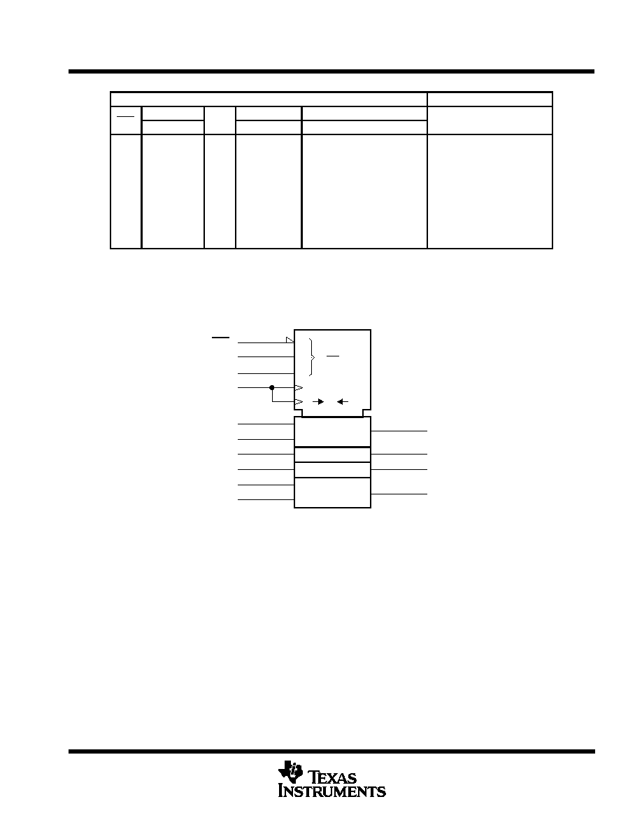
FUNCTION TABLE
INPUTS
OUTPUTS
CLR
MODE
CLK
SERIAL
PARALLEL
QA
QB
QC
QD
CLR
S1
S0
CLK
LEFT
RIGHT
A
B
C
D
QA
QB
QC
QD
L
X
X
X
X
X
X
X
X
X
L
L
L
L
H
X
X
L
X
X
X
X
X
X
QA0
QB0
QC0
QD0
H
H
H
X
X
a
b
c
d
a
b
c
d
H
L
H
X
H
X
X
X
X
H
QAn
QBn
QCn
H
L
H
X
L
X
X
X
X
L
QAn
QBn
QCn
H
H
L
H
X
X
X
X
X
QBn
QCn
QDn
H
H
H
L
L
X
X
X
X
X
QBn
QCn
QDn
L
H
L
L
X
X
X
X
X
X
X
QA0
QB0
QC0
QD0
H = high level (steady state); L = low level (steady state); X = irrelevant (any input, including transitions);
= transition from
low to high level; a, b, c, d = the level of steady-state input at inputs A, B, C, or D, respectively; QA0, QB0, QC0, QD0 = the
level of QA, QB, QC, or QD, respectively, before the indicated steady-state input conditions were established; QAn, QBn, QCn,
QDn = the level of QA, QB, QC, respectively, before the most recent
transition of the clock.
logic symbol
SRG4
3, 4D
4
B
3, 4D
5
C
3, 4D
6
D
2, 4D
7
SL SER
1, 4D
2
SR SER
3, 4D
3
A
R
1
11
CLK
C4
M
0
3
14
13
15
1
10
S1
0
9
S0
1 /2
12
CLR
QA
QB
QC
QD
This symbol is in accordance with ANSI/IEEE Std 91-1984 and IEC Publication 617-12.
SN54AS194, SN74AS194
4-BIT BIDIRECTIONAL UNIVERSAL SHIFT REGISTERS
SDAS212A DECEMBER 1983 REVISED DECEMBER 1994
3
POST OFFICE BOX 655303
·
DALLAS, TEXAS 75265
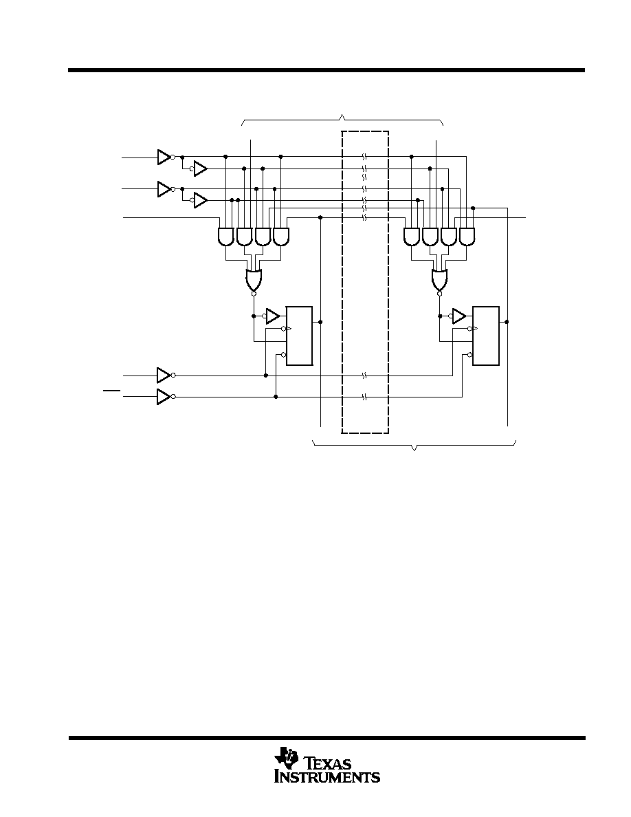
logic diagram (positive logic)
C1
1S
Two
Identical
Channels
Not
Shown
9
2
11
7
S0
S1
SR SER
SL SER
QA
QD
1
CLR
10
1R
CLK
R
C1
1S
1R
R
A
D
3
6
15
12
Parallel Inputs
Parallel Outputs
I/O ports not shown: QB (14) and QC (13)
Pin numbers shown are for the D, J, and N packages.
SN54AS194, SN74AS194
4-BIT BIDIRECTIONAL UNIVERSAL SHIFT REGISTERS
SDAS212A DECEMBER 1983 REVISED DECEMBER 1994
4
POST OFFICE BOX 655303
·
DALLAS, TEXAS 75265
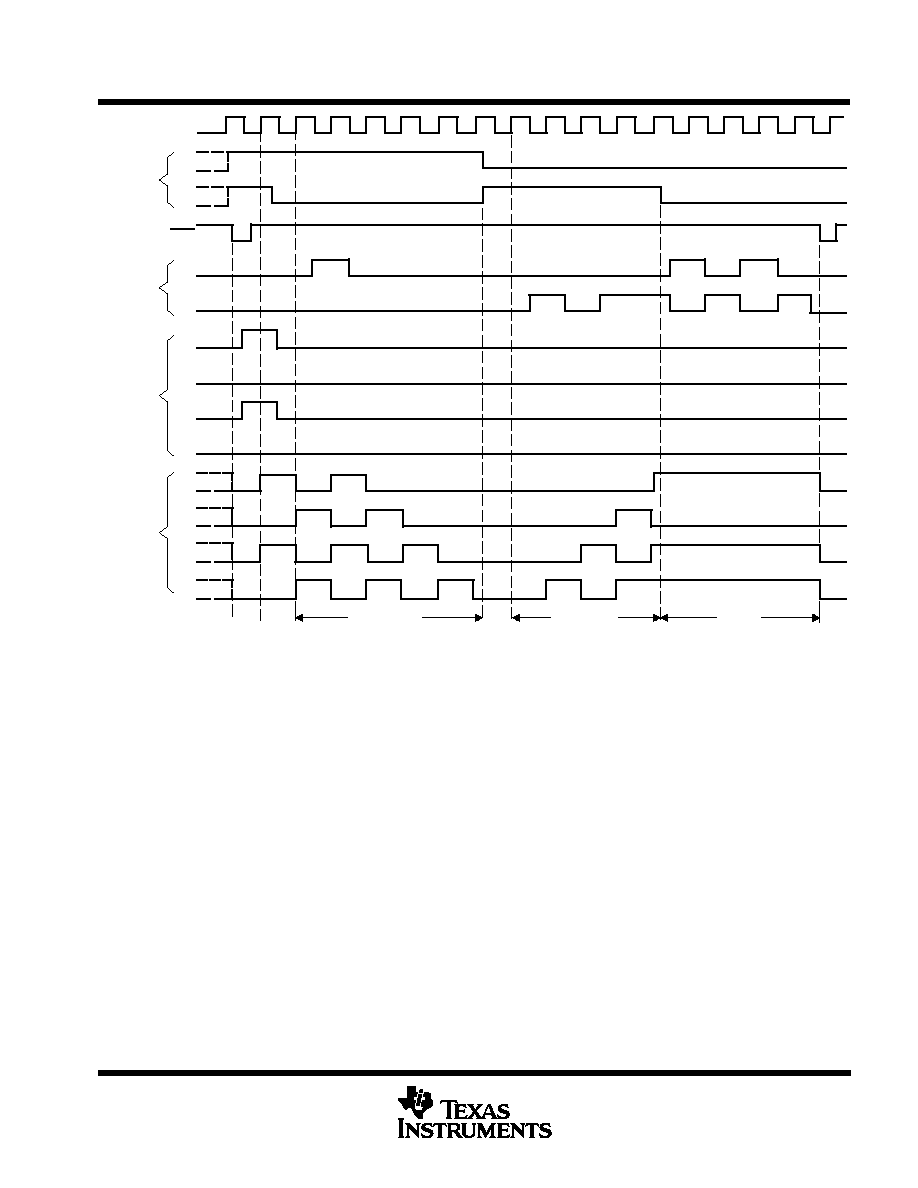
Shift Left
Clear
Inhibit
Shift Right
Clear Load
L
H
L
H
Mode-
Control
Inputs
Serial
Data
Inputs
Parallel
Data
Inputs
Outputs
CLK
S0
S1
CLR
R
L
A
B
C
D
QA
QB
QC
QD
Figure 1. Typical Clear, Load, Right-Shift, and Clear Sequences
absolute maximum ratings over operating free-air temperature range (unless otherwise noted)
Supply voltage, V
CC
7 V
. . . . . . . . . . . . . . . . . . . . . . . . . . . . . . . . . . . . . . . . . . . . . . . . . . . . . . . . . . . . . . . . . . . . . . . .
Input voltage, V
I
7 V
. . . . . . . . . . . . . . . . . . . . . . . . . . . . . . . . . . . . . . . . . . . . . . . . . . . . . . . . . . . . . . . . . . . . . . . . . . . .
Operating free-air temperature range, T
A
: SN54AS194
55
°
C to 125
°
C
. . . . . . . . . . . . . . . . . . . . . . . . . . . . . .
SN74AS194
0
°
C to 70
°
C
. . . . . . . . . . . . . . . . . . . . . . . . . . . . . . . . . .
Storage temperature range
65
°
C to 150
°
C
. . . . . . . . . . . . . . . . . . . . . . . . . . . . . . . . . . . . . . . . . . . . . . . . . . . . . . .
Stresses beyond those listed under "absolute maximum ratings" may cause permanent damage to the device. These are stress ratings only, and
functional operation of the device at these or any other conditions beyond those indicated under "recommended operating conditions" is not
implied. Exposure to absolute-maximum-rated conditions for extended periods may affect device reliability.
SN54AS194, SN74AS194
4-BIT BIDIRECTIONAL UNIVERSAL SHIFT REGISTERS
SDAS212A DECEMBER 1983 REVISED DECEMBER 1994
5
POST OFFICE BOX 655303
·
DALLAS, TEXAS 75265
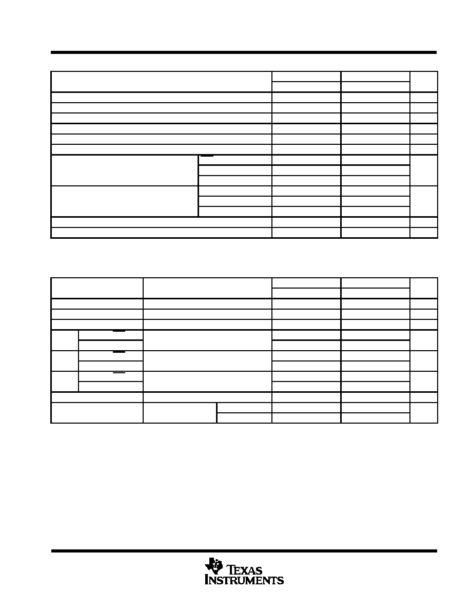
recommended operating conditions
SN54AS194
SN74AS194
UNIT
MIN
NOM
MAX
MIN
NOM
MAX
UNIT
VCC
Supply voltage
4.5
5
5.5
4.5
5
5.5
V
VIH
High-level input voltage
2
2
V
VIL
Low-level input voltage
0.8
0.8
V
IOH
High-level output current
2
2
mA
IOL
Low-level output current
20
20
mA
fclock*
Clock frequency
0
75
0
80
MHz
CLR
4
4.5
tw*
Pulse duration
CLK high
4
4
ns
CLK low
6
7
Select
9
9.5
tsu*
Setup time before CLK
Data
3.5
4
ns
Clear inactive state
6
6
th*
Hold time, data after CLK
0.5
0.5
ns
TA
Operating free-air temperature
55
125
0
70
°
C
* On products compliant to MIL-STD-883, Class B, these parameters are based on characterization data, but are not production tested.
electrical characteristics over recommended operating free-air temperature range (unless
otherwise noted)
PARAMETER
TEST CONDITIONS
SN54AS194
SN74AS194
UNIT
PARAMETER
TEST CONDITIONS
MIN
TYP
MAX
MIN
TYP
MAX
UNIT
VIK
VCC = 4.5 V,
II = 18 mA
1.2
1.2
V
VOH
VCC = 4.5 V to 5.5 V,
IOH = 2 mA
VCC 2
VCC 2
V
VOL
VCC = 4.5 V,
IOL = 20 mA
0.35
0.5
0.35
0.5
V
II
Data, CLK, CLR
VCC = 5 5 V
VI = 7 V
0.1
0.1
mA
II
Mode, SL, SR
VCC = 5.5 V,
VI = 7 V
0.2
0.2
mA
IIH
Data, CLK, CLR
VCC = 5 5 V
VI = 2 7 V
20
20
µ
A
IIH
Mode, SL, SR
VCC = 5.5 V,
VI = 2.7 V
40
40
µ
A
IIL
Data, CLK, CLR
VCC = 5 5 V
VI = 0 4 V
0.5
0.5
mA
IIL
Mode, SL, SR
VCC = 5.5 V,
VI = 0.4 V
1
1
mA
IO
VCC = 5.5 V,
VO = 2.25 V
30
112
30
112
mA
ICC
VCC = 5 5 V
Outputs high
30
49
30
43
mA
ICC
VCC = 5.5 V
Outputs low
38
60
38
53
mA
All typical values are at VCC = 5 V, TA = 25
°
C.
The output conditions have been chosen to produce a current that closely approximates one half of the true short-circuit output current, IOS.