Äîêóìåíòàöèÿ è îïèñàíèÿ www.docs.chipfind.ru
SN54ALS299, SN74ALS299
8-BIT UNIVERSAL SHIFT/STORAGE REGISTERS
WITH 3-STATE OUTPUTS
SDAS220B DECEMBER 1982 REVISED DECEMBER 1994
Copyright
©
1994, Texas Instruments Incorporated
1
POST OFFICE BOX 655303
·
DALLAS, TEXAS 75265
·
Multiplexed I/O Ports Provide Improved Bit
Density
·
Four Modes of Operation:
Hold (Store)
Shift Right
Shift Left
Load Data
·
Operate With Outputs Enabled or at High
Impedance
·
3-State Outputs Drive Bus Lines Directly
·
Can Be Cascaded for n-Bit Word Lengths
·
Direct Overriding Clear
·
Applications:
Stacked or Push-Down Registers
Buffer Storage
Accumulator Registers
·
Package Options Include Plastic
Small-Outline (DW) Packages, Ceramic
Chip Carriers (FK), and Standard Plastic (N)
and Ceramic (J) 300-mil DIPs
description
These 8-bit universal shift /storage registers
feature multiplexed I/O ports to achieve full 8-bit
data handling in a single 20-pin package. Two
function-select (S0, S1) inputs and two output-
enable (OE1, OE2) inputs can be used to choose
the modes of operation listed in the function table.
Synchronous parallel loading is accomplished by taking both S0 and S1 high. This places the 3-state outputs
in the high-impedance state and permits data applied on the I/O ports to be clocked into the register. Reading
out of the register can be accomplished while the outputs are enabled in any mode. Clearing occurs
asynchronously when the clear (CLR) input is low. Taking either OE1 or OE2 high disables the outputs, but has
no effect on clearing, shifting, or storing data.
The SN54ALS299 is characterized for operation over the full military temperature range of 55
°
C to 125
°
C. The
SN74ALS299 is characterized for operation from 0
°
C to 70
°
C.
1
2
3
4
5
6
7
8
9
10
20
19
18
17
16
15
14
13
12
11
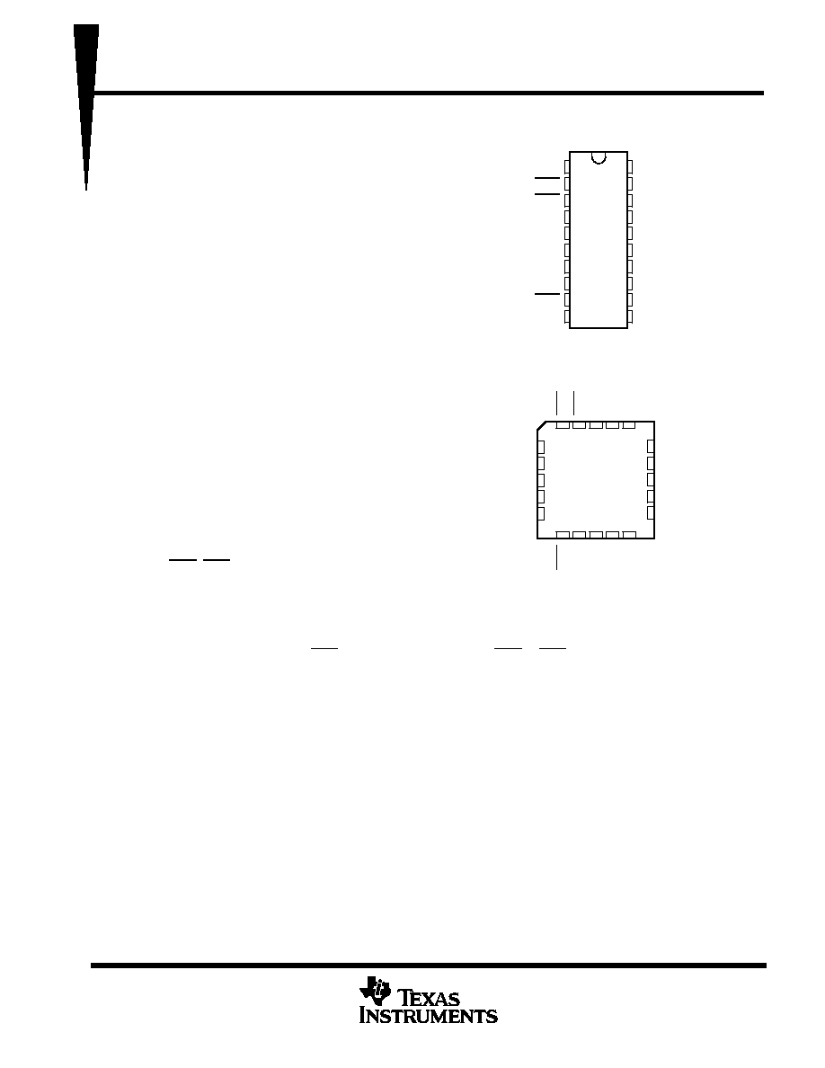
S0
OE1
OE2
G/Q
G
E/Q
E
C/Q
C
A/Q
A
Q
A
CLR
GND
V
CC
S1
SL
Q
H
H/Q
H
F/Q
F
D/Q
D
B/Q
B
CLK
SR
SN54ALS299 . . . J PACKAGE
SN74ALS299 . . . DW OR N PACKAGE
(TOP VIEW)
3
2 1 20 19
9 10 11 12 13
4
5
6
7
8
18
17
16
15
14
SL
Q
H
H/Q
H
F/Q
F
D/Q
D
G/Q
G
E/Q
E
C/Q
C
A/Q
A
Q
A
OE2
OE1
S0
CLK
B/Q
S1
CLR
GND
SR
V
CC
SN54ALS299 . . . FK PACKAGE
(TOP VIEW)
B
PRODUCTION DATA information is current as of publication date.
Products conform to specifications per the terms of Texas Instruments
standard warranty. Production processing does not necessarily include
testing of all parameters.
SN54ALS299, SN74ALS299
8-BIT UNIVERSAL SHIFT/STORAGE REGISTERS
WITH 3-STATE OUTPUTS
SDAS220B DECEMBER 1982 REVISED DECEMBER 1994
2
POST OFFICE BOX 655303
·
DALLAS, TEXAS 75265
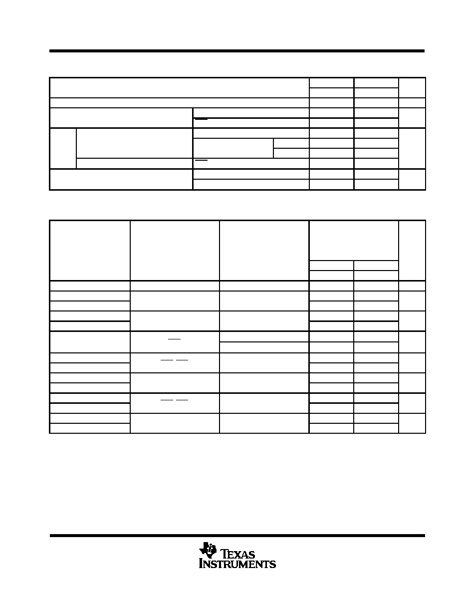
FUNCTION TABLE
MODE
INPUTS
I/O PORTS
OUTPUTS
MODE
CLR
S1
S0
OE1
OE2
CLK
SL
SR
A/QA B/QB C/QC D/QD E/QE
F/QF G/QG H/QH
QA
QH
Clear
L
L
L
X
L
H
L
X
H
L
L
X
L
L
X
X
X
X
X
X
X
X
X
X
L
L
X
L
L
X
L
L
X
L
L
X
L
L
X
L
L
X
L
L
X
L
L
X
L
L
L
L
L
L
Hold
H
H
L
X
L
X
L
L
L
L
X
L
X
X
X
X
QA0
QA0
QB0
QB0
QC0
QC0
QD0
QD0
QE0
QE0
QF0
QF0
QG0
QG0
QH0
QH0
QA0
QA0
QH0
QH0
Shift
Right
H
H
L
L
H
H
L
L
L
L
X
X
H
L
H
L
QAn
QAn
QBn
QBn
QCn
QCn
QDn
QDn
QEn
QEn
QFn
QFn
QGn
QGn
H
L
QGn
QGn
Shift
Left
H
H
H
H
L
L
L
L
L
L
H
L
X
X
QBn
QBn
QCn
QCn
QDn
QDn
QEn
QEn
QFn
QFn
QGn
QGn
QHn
QHn
H
L
QBn
QBn
H
L
Load
H
H
H
X
X
X
X
a
b
c
d
e
f
g
h
a
h
NOTE: a . . . h = the level of the steady-state input at inputs A through H, respectively. This data is loaded into the flip-flops while the flip-flop outputs
are isolated from the I/O terminals.
When one or both output-enable inputs are high, the eight I/O terminals are disabled to the high-impedance state; however, sequential operation
or clearing of the register is not affected.
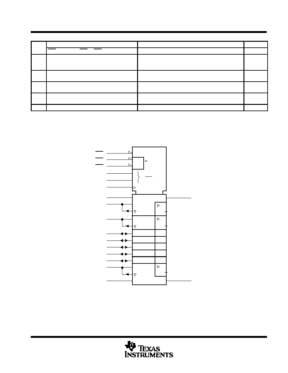
logic symbol
SRG8
M
0
3
R
9
6
14
5
15
4
8
2
3
0
1
S0
1
19
S1
12
CLK
5, 13
1,4D
11
SR
3,4D
7
6, 13
3,4D
13
17
12, 13
2,4D
18
SL
3,4D
16
&
3EN13
C4/1
/2
QA
QH
CLR
OE1
OE2
A /QA
H/QH
B/QB
C/QC
D/QD
E/QE
F/QF
G/QG
Z5
Z6
Z12
This symbol is in accordance with ANSI/IEEE Std 91-1984 and IEC Publication 617-12.
SN54ALS299, SN74ALS299
8-BIT UNIVERSAL SHIFT/STORAGE REGISTERS
WITH 3-STATE OUTPUTS
SDAS220B DECEMBER 1982 REVISED DECEMBER 1994
3
POST OFFICE BOX 655303
·
DALLAS, TEXAS 75265
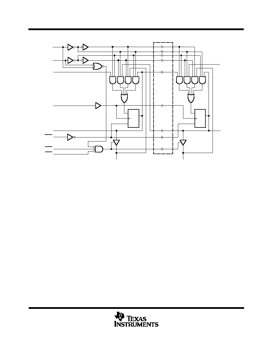
logic diagram (positive logic)
C1
1D
C1
1D
Six
Identical
Channels
Not
Shown
19
11
12
8
2
3
18
17
S0
S1
SR
(shift right
serial input)
CLK
QA
OE1
OE2
SL
(shift left
serial input)
QH
7
16
A /QA
H /QH
9
CLR
1
R
R
I/O ports not shown: B/QB (13), C/QC (6), D/QD (14), E/QE (5), F/QF (15), and G/QG (4).
absolute maximum ratings over operating free-air temperature range (unless otherwise noted)
Supply voltage, V
CC
7 V
. . . . . . . . . . . . . . . . . . . . . . . . . . . . . . . . . . . . . . . . . . . . . . . . . . . . . . . . . . . . . . . . . . . . . . . .
Input voltage, V
I
: All inputs
7 V
. . . . . . . . . . . . . . . . . . . . . . . . . . . . . . . . . . . . . . . . . . . . . . . . . . . . . . . . . . . . . . . . . . .
I/O ports
5.5 V
. . . . . . . . . . . . . . . . . . . . . . . . . . . . . . . . . . . . . . . . . . . . . . . . . . . . . . . . . . . . . . . . .
Operating free-air temperature range, T
A
: SN54ALS299
55
°
C to 125
°
C
. . . . . . . . . . . . . . . . . . . . . . . . . . . . .
SN74ALS299
0
°
C to 70
°
C
. . . . . . . . . . . . . . . . . . . . . . . . . . . . . . . . .
Storage temperature range
65
°
C to 150
°
C
. . . . . . . . . . . . . . . . . . . . . . . . . . . . . . . . . . . . . . . . . . . . . . . . . . . . . . .
Stresses beyond those listed under "absolute maximum ratings" may cause permanent damage to the device. These are stress ratings only, and
functional operation of the device at these or any other conditions beyond those indicated under "recommended operating conditions" is not
implied. Exposure to absolute-maximum-rated conditions for extended periods may affect device reliability.
SN54ALS299, SN74ALS299
8-BIT UNIVERSAL SHIFT/STORAGE REGISTERS
WITH 3-STATE OUTPUTS
SDAS220B DECEMBER 1982 REVISED DECEMBER 1994
4
POST OFFICE BOX 655303
·
DALLAS, TEXAS 75265
recommended operating conditions
SN54ALS299
SN74ALS299
UNIT
MIN
NOM
MAX
MIN
NOM
MAX
UNIT
VCC
Supply voltage
4.5
5
5.5
4.5
5
5.5
V
VIH
High-level input voltage
2
2
V
VIL
Low-level input voltage
0.7
0.8
V
IOH
High level output current
QA
or QH
0.4
0.4
mA
IOH
High-level output current
QA QH
1
2.6
mA
IOL
Low level output current
QA
or QH
4
8
mA
IOL
Low-level output current
QA QH
12
24
mA
TA
Operating free-air temperature
55
125
0
70
°
C
electrical characteristics over recommended operating free-air temperature range (unless
otherwise noted)
PARAMETER
TEST CONDITIONS
SN54ALS299
SN74ALS299
UNIT
PARAMETER
TEST CONDITIONS
MIN
TYP
MAX
MIN
TYP
MAX
UNIT
VIK
VCC = 4.5 V,
II = 18 mA
1.5
1.5
V
All outputs
VCC = 4.5 V to 5.5 V,
IOH = 0.4 mA
VCC 2
VCC 2
VOH
QA QH
VCC = 4 5 V
IOH = 1 mA
2.4
3.3
V
QA QH
VCC = 4.5 V
IOH = 2.6 mA
2.4
3.2
QA
or QH
VCC = 4 5 V
IOL = 4 mA
0.25
0.4
0.25
0.4
VOL
QA
or QH
VCC = 4.5 V
IOL = 8 mA
0.35
0.5
V
VOL
QA QH
VCC = 4 5 V
IOL = 12 mA
0.25
0.4
0.25
0.4
V
QA QH
VCC = 4.5 V
IOL = 24 mA
0.35
0.5
II
A H
VCC = 5 5 V
VI = 5.5 V
0.1
0.1
mA
II
Any others
VCC = 5.5 V
VI = 7 V
0.1
0.1
mA
IIH
VCC = 5.5 V,
VI = 2.7 V
20
20
µ
A
I
S0, S1, SR, SL
VCC = 5 5 V
VI = 0 4 V
0.2
0.2
mA
IIL
Any others
VCC = 5.5 V,
VI = 0.4 V
0.1
0.1
mA
I §
QA
or QH
VCC = 5 5 V
VO = 2 25 V
15
70
15
70
mA
IO§
QA QH
VCC = 5.5 V,
VO = 2.25 V
20
112
30
112
mA
Outputs high
15
28
15
28
ICC
VCC = 5.5 V
Outputs low
22
38
22
38
mA
Outputs disabled
23
40
23
40
All typical values are at VCC = 5 V, TA = 25
°
C.
For I/O ports (QAQH), the parameters IIH and IIL include the off-state output current.
§ The output conditions have been chosen to produce a current that closely approximates one half of the true short-circuit output current, IOS.
SN54ALS299, SN74ALS299
8-BIT UNIVERSAL SHIFT/STORAGE REGISTERS
WITH 3-STATE OUTPUTS
SDAS220B DECEMBER 1982 REVISED DECEMBER 1994
5
POST OFFICE BOX 655303
·
DALLAS, TEXAS 75265
timing requirements over recommended ranges of supply voltage and operating free-air
temperature (unless otherwise noted)
SN54ALS299
SN74ALS299
UNIT
MIN
MAX
MIN
MAX
UNIT
fclock
Clock frequency (at 50% duty cycle)
0
17
0
30
MHz
t
Pulse duration
CLK high or low
22
16.5
ns
tw
Pulse duration
CLR low
12
10
ns
S0 or S1
25
20
t
Setup time before CLK
Serial or parallel data
High
18
16
ns
tsu
Serial or parallel data
Low
15
6
ns
Inactive-state setup time before CLK
CLR
15
15
th
Hold time after CLK
S0 or S1
0
0
ns
th
Hold time after CLK
Serial or parallel data
0
0
ns
Inactive-state setup time is also referred to as recovery time.
switching characteristics (see Figure 1)
PARAMETER
FROM
(INPUT)
TO
(OUTPUT)
VCC = 4.5 V to 5.5 V,
CL = 50 pF,
R1 = 500
,
R2 = 500
,
TA = MIN to MAX
UNIT
SN54ALS299
SN74ALS299
MIN
MAX
MIN
MAX
fmax
17
30
MHz
tPLH
CLK
Q
Q
2
19
4
13
ns
tPHL
CLK
QA QH
4
25
7
19
ns
tPLH
CLK
Q
or Q
2
21
5
15
ns
tPHL
CLK
QA
or QH
4
25
8
18
ns
tPHL
CLR
QA QH
6
29
6
22
ns
tPHL
CLR
QA
or QH
6
29
6
22
ns
tPZH
OE1 OE2
Q
Q
5
22
6
16
ns
tPZL
OE1, OE2
QA QH
6
27
8
22
ns
tPZH
S0 S1
Q
Q
5
27
7
17
ns
tPZL
S0, S1
QA QH
6
26
8
22
ns
tPHZ
OE1 OE2
Q
Q
1
15
1
8
ns
tPLZ
OE1, OE2
QA QH
4
38
5
15
ns
tPHZ
S0 S1
QA QH
1
16
1
12
ns
tPLZ
S0, S1
QA QH
4
34
8
25
ns
For conditions shown as MIN or MAX, use the appropriate value specified under recommended operating conditions.