Äîêóìåíòàöèÿ è îïèñàíèÿ www.docs.chipfind.ru
SN54ALS165, SN74ALS165
PARALLEL-LOAD 8-BIT REGISTERS
SDAS157B JUNE 1982 REVISED DECEMBER 1994
Copyright
©
1994, Texas Instruments Incorporated
1
POST OFFICE BOX 655303
·
DALLAS, TEXAS 75265
·
Complementary Outputs
·
Direct Overriding Load (Data) Inputs
·
Gated Clock Inputs
·
Parallel-to-Serial Data Conversion
·
Package Options Include Plastic
Small-Outline (D) Packages, Ceramic Chip
Carriers (FK), and Standard Plastic (N) and
Ceramic (J) 300-mil DIPs
description
The
ALS165 are parallel-load 8-bit serial shift
registers that, when clocked, shift the data toward
serial (Q
H
and Q
H
) outputs. Parallel-in access to
each stage is provided by eight individual direct
data (A H) inputs that are enabled by a low level
at the shift/load (SH/LD) input. The
ALS165 have
a clock-inhibit function and complemented serial
outputs.
Clocking is accomplished by a low-to-high
transition of the clock (CLK) input while SH/LD is
held high and the clock inhibit (CLK INH) input is
held low. The functions of CLK and CLK INH are
interchangeable. Since a low CLK and a
low-to-high transition of CLK INH also
accomplishes clocking, CLK INH should be
changed to the high level only while CLK is high.
Parallel loading is inhibited when SH/LD is held
high. The parallel inputs to the register are
enabled while SH/LD is low independently of the
levels of the CLK, CLK INH, or serial (SER) inputs.
The SN54ALS165 is characterized for operation over the full military temperature range of 55
°
C to 125
°
C. The
SN74ALS165 is characterized for operation from 0
°
C to 70
°
C.
FUNCTION TABLE
INPUTS
FUNCTION
SH/LD
CLK
CLK INH
FUNCTION
L
X
X
Parallel load
H
H
X
No change
H
X
H
No change
H
L
Shift
H
L
Shift
Shift = content of each internal register shifts
toward serial outputs. Data at SER is shifted
into first register.
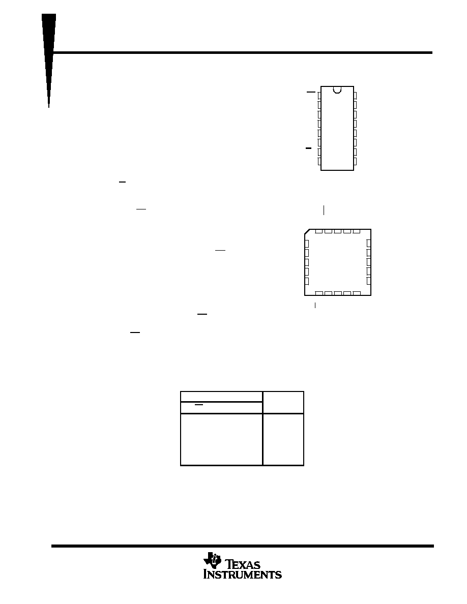
SN54ALS165 . . . J PACKAGE
SN74ALS165 . . . D OR N PACKAGE
(TOP VIEW)
3
2
1 20 19
9 10 11 12 13
4
5
6
7
8
18
17
16
15
14
D
C
NC
B
A
E
F
NC
G
H
SN54ALS165 . . . FK PACKAGE
(TOP VIEW)
CLK
SH/LD
NC
SER
CLK INH
H
GND
NC
NC No internal connection
V
CC
1
2
3
4
5
6
7
8
16
15
14
13
12
11
10
9
SH/LD
CLK
E
F
G
H
Q
H
GND
V
CC
CLK INH
D
C
B
A
SER
Q
H
Q
H
Q
PRODUCTION DATA information is current as of publication date.
Products conform to specifications per the terms of Texas Instruments
standard warranty. Production processing does not necessarily include
testing of all parameters.
SN54ALS165, SN74ALS165
PARALLEL-LOAD 8-BIT REGISTERS
SDAS157B JUNE 1982 REVISED DECEMBER 1994
2
POST OFFICE BOX 655303
·
DALLAS, TEXAS 75265
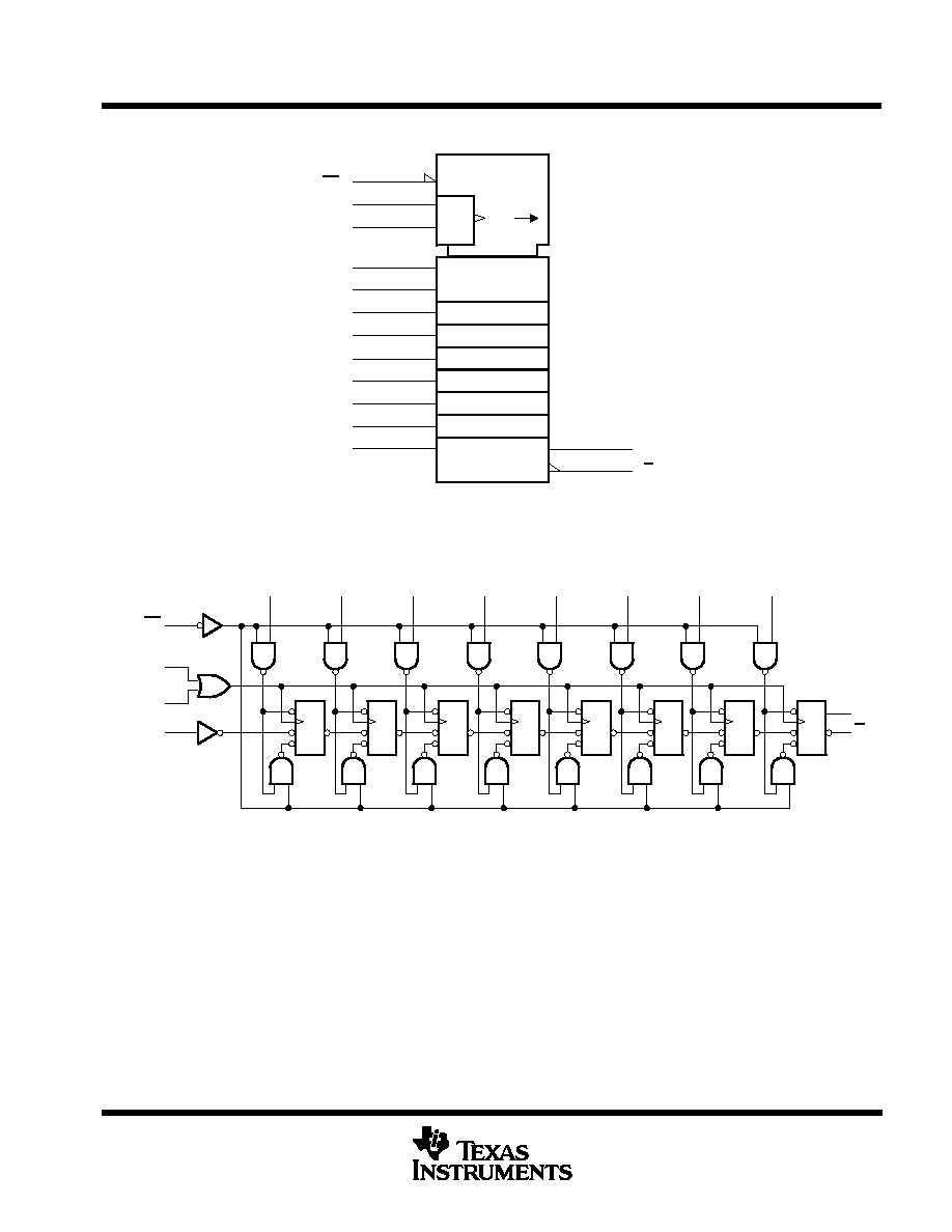
logic symbol
SRG8
C1 [LOAD]
1
15
CLK INH
2
CLK
14
D
2D
10
SER
1D
11
A
1D
12
B
13
C
3
E
4
F
5
G
1D
6
H
C2/
7
9
1
SH/LD
QH
QH
This symbol is in accordance with ANSI/IEEE Std 91-1984 and IEC Publication 617-12.
Pin numbers shown are for the D, J, and N packages.
logic diagram (positive logic)
S
1D
R
C1
S
1D
R
C1
S
1D
R
C1
S
1D
R
C1
S
1D
R
C1
S
1D
R
C1
S
1D
R
C1
S
1D
R
C1
1
15
2
10
SH/LD
CLK INH
CLK
SER
9
7
QH
QH
11
12
13
14
3
4
5
6
A
B
C
D
E
F
G
H
Pin numbers shown are for the D, J, and N packages.
SN54ALS165, SN74ALS165
PARALLEL-LOAD 8-BIT REGISTERS
SDAS157B JUNE 1982 REVISED DECEMBER 1994
3
POST OFFICE BOX 655303
·
DALLAS, TEXAS 75265
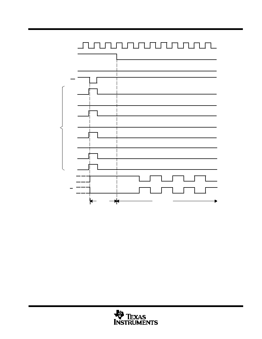
typical shift, load, and inhibit sequences
Load
E
QH
H
G
C
F
Data
Inputs
D
SH/LD
SER
CLK INH
CLK
B
A
QH
L
L
H
L
H
L
H
H
H
H
L
H
L
H
L
H
L
H
L
L
H
L
H
L
H
Inhibit
Serial Shift
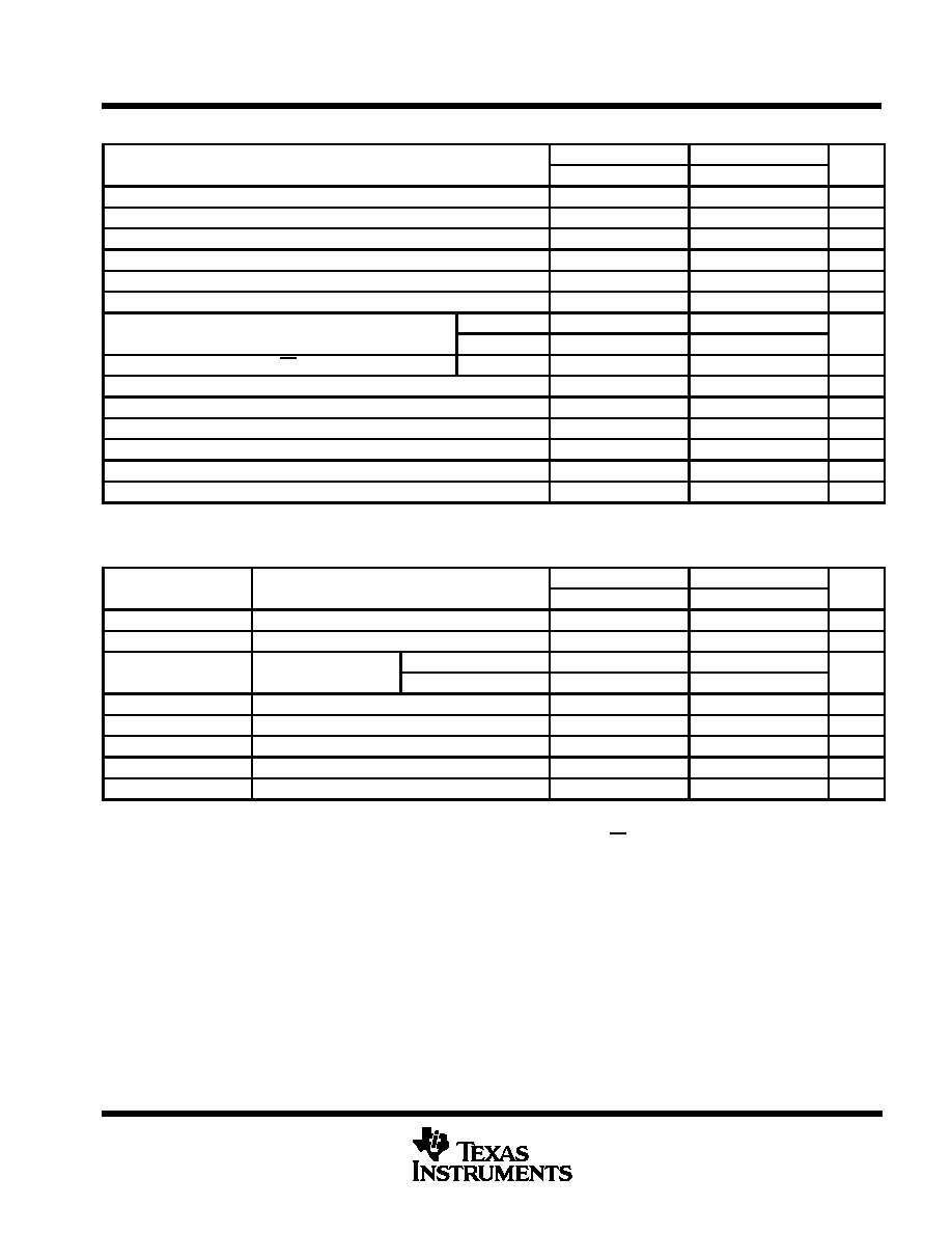
absolute maximum ratings over operating free-air temperature range (unless otherwise noted)
Supply voltage, V
CC
7 V
. . . . . . . . . . . . . . . . . . . . . . . . . . . . . . . . . . . . . . . . . . . . . . . . . . . . . . . . . . . . . . . . . . . . . . . .
Input voltage, V
I
7 V
. . . . . . . . . . . . . . . . . . . . . . . . . . . . . . . . . . . . . . . . . . . . . . . . . . . . . . . . . . . . . . . . . . . . . . . . . . . .
Operating free-air temperature range, T
A
: SN54ALS165
55
°
C to 125
°
C
. . . . . . . . . . . . . . . . . . . . . . . . . . . . .
SN74ALS165
0
°
C to 70
°
C
. . . . . . . . . . . . . . . . . . . . . . . . . . . . . . . . .
Storage temperature range
65
°
C to 150
°
C
. . . . . . . . . . . . . . . . . . . . . . . . . . . . . . . . . . . . . . . . . . . . . . . . . . . . . . .
Stresses beyond those listed under "absolute maximum ratings" may cause permanent damage to the device. These are stress ratings only, and
functional operation of the device at these or any other conditions beyond those indicated under "recommended operating conditions" is not
implied. Exposure to absolute-maximum-rated conditions for extended periods may affect device reliability.
SN54ALS165, SN74ALS165
PARALLEL-LOAD 8-BIT REGISTERS
SDAS157B JUNE 1982 REVISED DECEMBER 1994
4
POST OFFICE BOX 655303
·
DALLAS, TEXAS 75265
recommended operating conditions
SN54ALS165
SN74ALS165
UNIT
MIN
NOM
MAX
MIN
NOM
MAX
UNIT
VCC
Supply voltage
4.5
5
5.5
4.5
5
5.5
V
VIH
High-level input voltage
2
2
V
VIL
Low-level input voltage
0.7
0.8
V
IOH
High-level output current
0.4
0.4
mA
IOL
Low-level output current
4
8
mA
fclock
Clock frequency
0
35
0
45
MHz
t (CLK)
Pulse duration CLK (see Figure 1)
CLK high
14
11
ns
tw(CLK)
Pulse duration, CLK (see Figure 1)
CLK low
14
11
ns
tw(load)
Pulse duration, SH/LD low
CLK low
15
12
ns
tsu1
Setup time, clock enable (see Figure 1)
15
11
ns
tsu2
Setup time, parallel input (see Figure 1)
11
10
ns
tsu3
Setup time, serial input (see Figure 2)
11
10
ns
tsu4
Setup time, shift (see Figure 2)
15
10
ns
th
Hold time at any input
4
4
ns
TA
Operating free-air temperature
55
125
0
70
°
C
electrical characteristics over recommended operating free-air temperature range (unless
otherwise noted)
PARAMETER
TEST CONDITIONS
SN54ALS165
SN74ALS165
UNIT
PARAMETER
TEST CONDITIONS
MIN
TYP
MAX
MIN
TYP
MAX
UNIT
VIK
VCC = 4.5 V,
II = 18 mA
1.5
1.5
V
VOH
VCC = 4.5 V to 5.5 V,
IOH = 0.4 mA
VCC 2
VCC 2
V
VOL
VCC = 4 5 V
IOL = 4 mA
0.25
0.4
0.25
0.4
V
VOL
VCC = 4.5 V
IOL = 8 mA
0.35
0.5
V
II
VCC = 5.5 V,
VI = 7 V
0.1
0.1
mA
IIH
VCC = 5.5 V,
VI = 2.7 V
20
20
µ
A
IIL
VCC = 5.5 V,
VI = 0.4 V
0.1
0.1
mA
IO
VCC = 5.5 V,
VO = 2.25 V
20
112
30
112
mA
ICC
VCC = 5.5 V,
See Note 1
12
24
12
24
mA
All typical values are at VCC = 5 V, TA = 25
°
C.
The output conditions have been chosen to produce a current that closely approximates one half of the true short-circuit output current, IOS.
NOTE 1: With the outputs open, CLK INH and CLK at 4.5 V, and a clock pulse applied to SH/LD, ICC is measured first with the parallel inputs at
4.5 V, then with the parallel inputs grounded.
SN54ALS165, SN74ALS165
PARALLEL-LOAD 8-BIT REGISTERS
SDAS157B JUNE 1982 REVISED DECEMBER 1994
5
POST OFFICE BOX 655303
·
DALLAS, TEXAS 75265
switching characteristics (see Figures 1, 2, and 3)
PARAMETER
FROM
(INPUT)
TO
(OUTPUT)
VCC = 4.5 V to 5.5 V,
CL = 50 pF,
RL = 500
,
TA = MIN to MAX
UNIT
(INPUT)
(OUTPUT)
SN54ALS165
SN74ALS165
MIN
MAX
MIN
MAX
fmax
35
45
MHz
tPLH
SH/LD
Any
4
23
4
20
ns
tPHL
SH/LD
Any
4
23
4
22
ns
tPLH
CLK
Any
3
14
3
13
ns
tPHL
CLK
Any
3
15
3
14
ns
tPLH
H
QH
3
14
3
13
ns
tPHL
H
QH
3
18
3
16
ns
tPLH
H
QH
2
17
2
15
ns
tPHL
H
QH
3
17
3
16
ns
For conditions shown as MIN or MAX, use the appropriate value specified under recommended operating conditions.
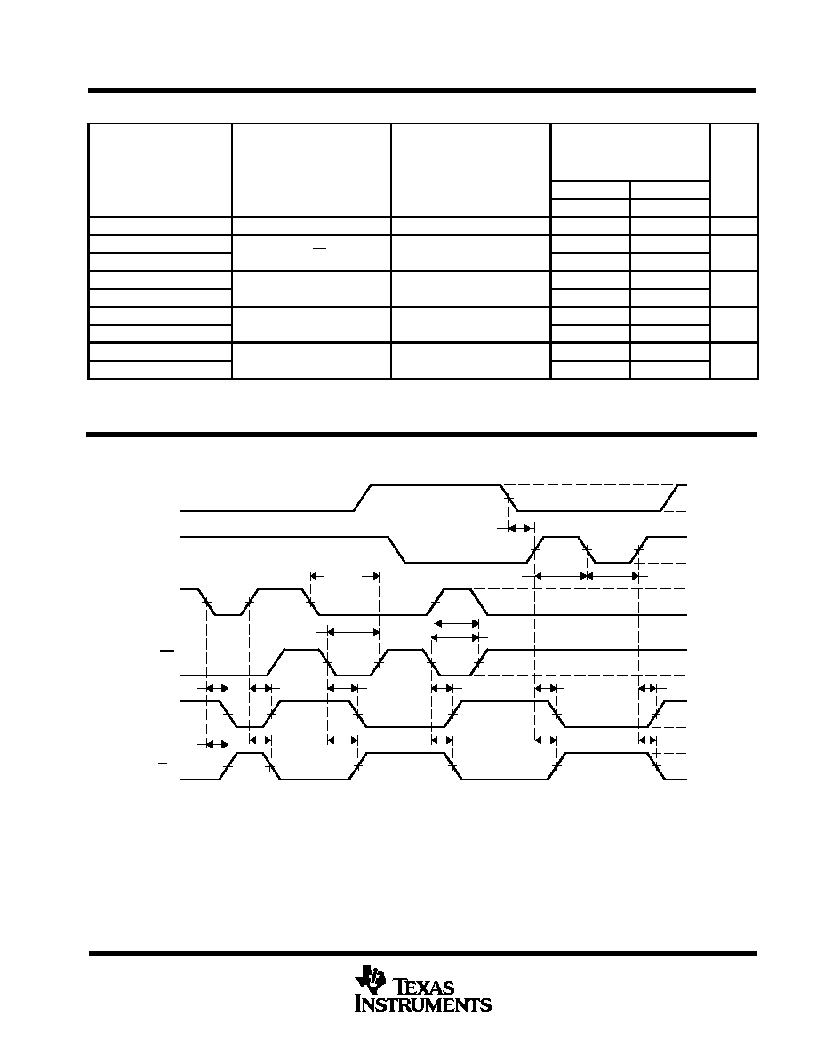
PARAMETER MEASUREMENT INFORMATION
tw(load)
tw(load)
(disable while
clock is high)
3.5 V
0.3 V
3.5 V
0.3 V
3.5 V
0.3 V
3.5 V
0.3 V
VOH
VOL
VOH
VOL
Vref
tsu1
tw(CLK)
tw(CLK)
tsu2
tsu2
Vref
tPHL
tPLH
tPHL
tPLH
tPHL
tPLH
Vref
Vref
tPLH
tPHL
tPLH
tPHL
tPLH
tPHL
Vref
CLK INH
CLK
F and H
Inputs
(see Notes
A and B)
SH/LD
Output
QH
Output
QH
Vref
Vref
Vref
Vref
Vref
Vref
Vref
Vref
Vref
Vref
Vref
Vref
Vref
Vref
Vref
Vref
Vref
Vref
NOTES: A. The remaining six data inputs and SER are low.
B. Prior to test, high-level data is loaded into the H input.
C. The input pulse generators have the following characteristics: PRR
1 MHz, duty cycle
50%, tr = tf = 2 ns.
D. Vref = 1.3 V
Figure 1. Voltage Waveforms