Äîêóìåíòàöèÿ è îïèñàíèÿ www.docs.chipfind.ru
For technical support and more information, see inside back cover or visit www.ti.com/powertrends
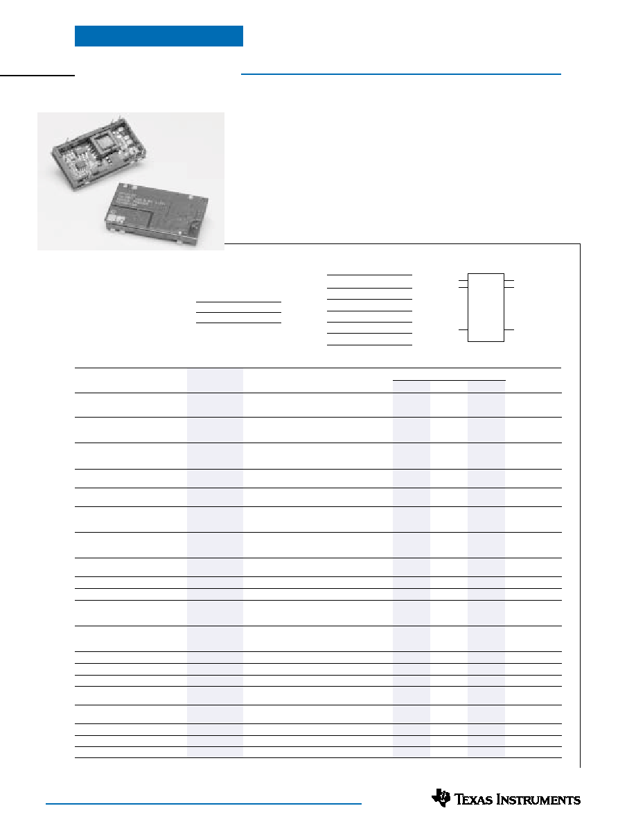
PT4210 Series --48V
Features
·
Wide Input Voltage Range:
38V to 75V
·
1,500 VDC Isolation
·
6 Pin DIP Package
·
Low-Profile (8mm)
·
Pin-compatible with PT4200 Series
·
No External Components Required
2
·
Safety Approvals --Pending
Description
The PT4210 series of low-power
isolated DC-DC converters are pin-
compatible with Power Trends' popular
PT4200 series. The PT4210 series has
improved load regulation over the
PT4200, and is a compatible alternative
for both new and existing designs.
Applications include Telecom and
Datacom systems where both board
space and height are a premium.
The PT4210 series is offered in both
through-hole or SMD-DIP package
types with single non-adjustable output
voltages of 3.3V, 5V, and 12V.
Ordering Information
PT4212
G = 3.3V/1.5A
PT4213
G = 5V/1.2A
PT4214
G = 12V/0.6A
Pin-Out Information
Pin
Function
1
+V
out
2
V
out
8
N/C
11
Remote On/Off
*
17
V
in
18
+V
in
5-7 Watt Low-Profile
Isolated DC-DC Converter
(For dimensions and PC board
layout, see Package Style 910)
Package Top View
SLTS137A
(Revised 4/19/2001)
PT4210
1 1
1 7
1 8
1
2
8
+Vin
Vin
R e m o t e
On/Off
*
+Vout
Vout
N/C
Package Suffix
(PT1234
X
)
Case/Pin
Configuration
Through-Hole
A
Surface Mount
C
Specifications
C
C
C
C
Characteristics
PT4210 SERIES
(T
a
= 25°C unless noted)
Symbols
Conditions
Min
Typ
Max
Units
Output Current
I
o
Over V
in
range
PT4212 (3.3V)
0
--
1.5
PT4213 (5.0V)
0
--
1.2
A
PT4214 ( 12V)
0
--
0.6
Output Voltage Tolerance
V
o
Over Vin range,
PT4212
3.17
--
3.5
10%I
o
max
I
o
I
o
max,
PT4213
4.85
--
5.25
V
40°C < T
a
<85°C
PT4214
11.5
--
12.5
Idling Voltage
V
o
I
o
= 0A
PT4212
--
3.7
3.9
PT4213
--
5.4
5.9
V
PT4214
--
12.7
17
Line Regulation
Reg
line
Over V
in
range @ max I
o
PT4212/4213
--
±20
--
mV
PT4214
--
±45
--
Load Regulation
Reg
load
V
in
=53V
PT4212/13
--
±100
--
mV
10%I
o
max
I
o
I
o
max
PT4214
--
±150
--
Current Limit
I
lim
Over V
in
range
PT4212
--
3.0
--
PT4213
--
3.0
A
PT4214
--
1.5
--
Short Circuit Current
I
sc
Over V
in
range
PT4212
--
2.4
--
PT4213
--
1.5
--
A
PT4214
--
1.0
--
Inrush Current
I
ir
V
in
= 53V @ max I
o
--
0.5
--
A
t
ir
On start-up
--
1.0
--
mSec
Input Voltage Range
V
in
Over I
o
range
38
--
75
V
V
o
Ripple/Noise
V
n
V
in
= 53V, I
o
=I
o
max
--
30
70
mV
pp
Transient Response
t
tr
V
in
=53V, 10%..100%I
o
max, 50% load step
--
200
--
µSec
V
o
over/undershoot:
PT4212/4213
--
+150/250
--
mV
PT4214
--
+250/500
--
Efficiency
V
in
=53V, I
o
=1.5A,
PT4212
--
80
--
V
in
=53V, I
o
=1.2A,
PT4213
--
82
--
%
V
in
=53V, I
o
=0.6A,
PT4214
--
84
--
Switching Frequency
o
Over V
in
and I
o
ranges
400
--
500
kHz
Operating Temperature
T
a
Over V
in
range
-40
--
+85
(1)
°C
Storage Temperature
T
s
--
-40
--
+125
°C
Mechanical Shock--
Per Mil-STD-202F, Method 213B,
--
TBD
--
G's
6mS half-sine, mounted to a PCB
Mechanical Vibration
--
Per Mil-STD-202F, Method 204D,
--
TBD
--
G's
10-500Hz, mounted to a PCB
Weight
--
--
--
10
--
grams
Isolation
--
--
1500
--
--
VDC
Flammability
--
Materials meet UL 94V-0
Notes: (1) See SOA curves or consult the factory for the appropriate derating.
(2) The maximum output capacitance must not exceed 150µF for the PT4212, 120µF for the PT4213, and 47µF for the PT4214.
For technical support and more information, see inside back cover or visit www.ti.com/powertrends
For technical support and more information, see inside back cover or visit www.ti.com/powertrends
For technical support and more information, see inside back cover or visit www.ti.com/powertrends
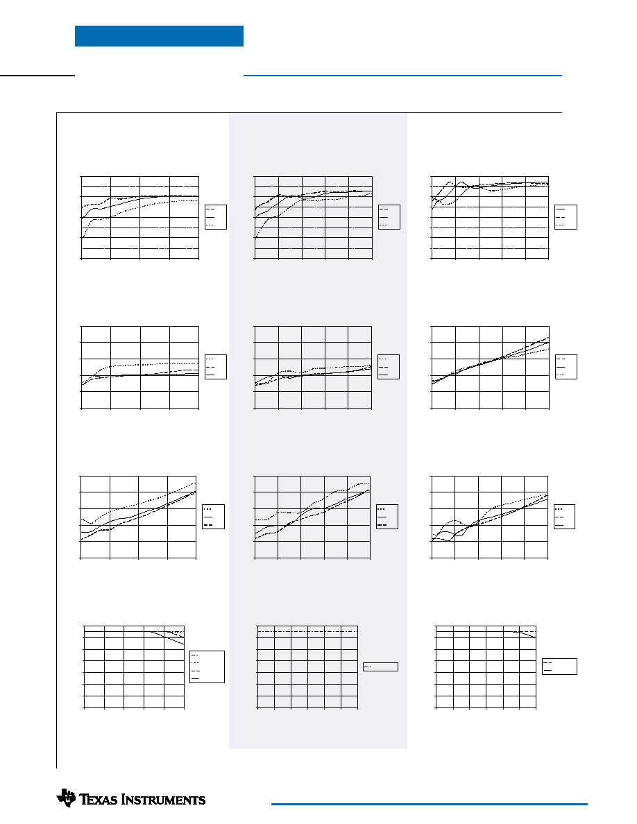
Typical Characteristics
PT4210 Series --48V
5-7 Watt Low-Profile
Isolated DC-DC Converter
PT4213 Performance
(See Note A)
Efficiency Vs Output Current
Power Dissipation Vs Output Current
Ripple Voltage Vs Output Current
Safe Operating Area, V
in
=3660V
PT4212 Performance
(See Note A)
PT4214 Performance
(See Note A)
Efficiency Vs Output Current
Efficiency Vs Output Current
Ripple Voltage Vs Output Current
Ripple Voltage Vs Output Current
Power Dissipation Vs Output Current
Power Dissipation Vs Output Current
Note A:
All Characteristic data in the above graphs has been developed from actual products tested at 25°C. This data is considered typical data for the converter.
Note B:
SOA curves represent operating conditions at which internal components are at or below manufacturer's maximum rated operating temperatures.
Safe Operating Area, V
in
=3660V
Safe Operating Area, V
in
=3660V
20.0
30.0
40.0
50.0
60.0
70.0
80.0
90.0
0.0
0.3
0.6
0.9
1.2
1.5
Iout (A)
Ambient Temperature (°C)
200LFM
120LFM
60LFM
Nat conv
Airflow
20.0
30.0
40.0
50.0
60.0
70.0
80.0
90.0
0.0
0.1
0.2
0.3
0.4
0.5
0.6
Iout (A)
Ambient Temperature (
°
C)
60LFM
Nat conv
Airflow
20.0
30.0
40.0
50.0
60.0
70.0
80.0
90.0
0.0
0.2
0.4
0.6
0.8
1.0
1.2
Iout (A)
Ambient Temperature (
°
C)
Nat conv
Airflow
50
60
70
80
90
0.1
0.2
0.3
0.4
0.5
0.6
Iout - (A)
Efficiency - %
53V
38V
75V
V
IN
0
10
20
30
40
50
0.1
0.2
0.3
0.4
0.5
0.6
Iout (A)
Ripple - mV
38V
53V
75V
V
IN
0
0.3
0.6
0.9
1.2
1.5
0.1
0.2
0.3
0.4
0.5
0.6
Iout (A)
Pd - Watts
75V
38V
53V
V
IN
50
60
70
80
90
0.2
0.4
0.6
0.8
1
1.2
Iout (A)
Efficiency - %
38V
53V
75V
V
IN
50
60
70
80
90
0.3
0.6
0.9
1.2
1.5
Iout (A)
Efficiency - %
38V
53V
75V
V
IN
0
10
20
30
40
50
0.3
0.6
0.9
1.2
1.5
Iout (A)
Ripple - mV
75V
38V
53V
V
IN
0
0.3
0.6
0.9
1.2
1.5
0.3
0.6
0.9
1.2
1.5
Iout (A)
Pd - Watts
75V
53V
38V
V
IN
0
10
20
30
40
50
0.2
0.4
0.6
0.8
1
1.2
Iout (A)
Ripple - mV
75V
38V
53V
V
IN
0
0.3
0.6
0.9
1.2
1.5
0.2
0.4
0.6
0.8
1
1.2
Iout (A)
Pd - Watts
75V
53V
38V
V
IN
Application Notes
For technical support and more information, see inside back cover or visit www.ti.com/powertrends
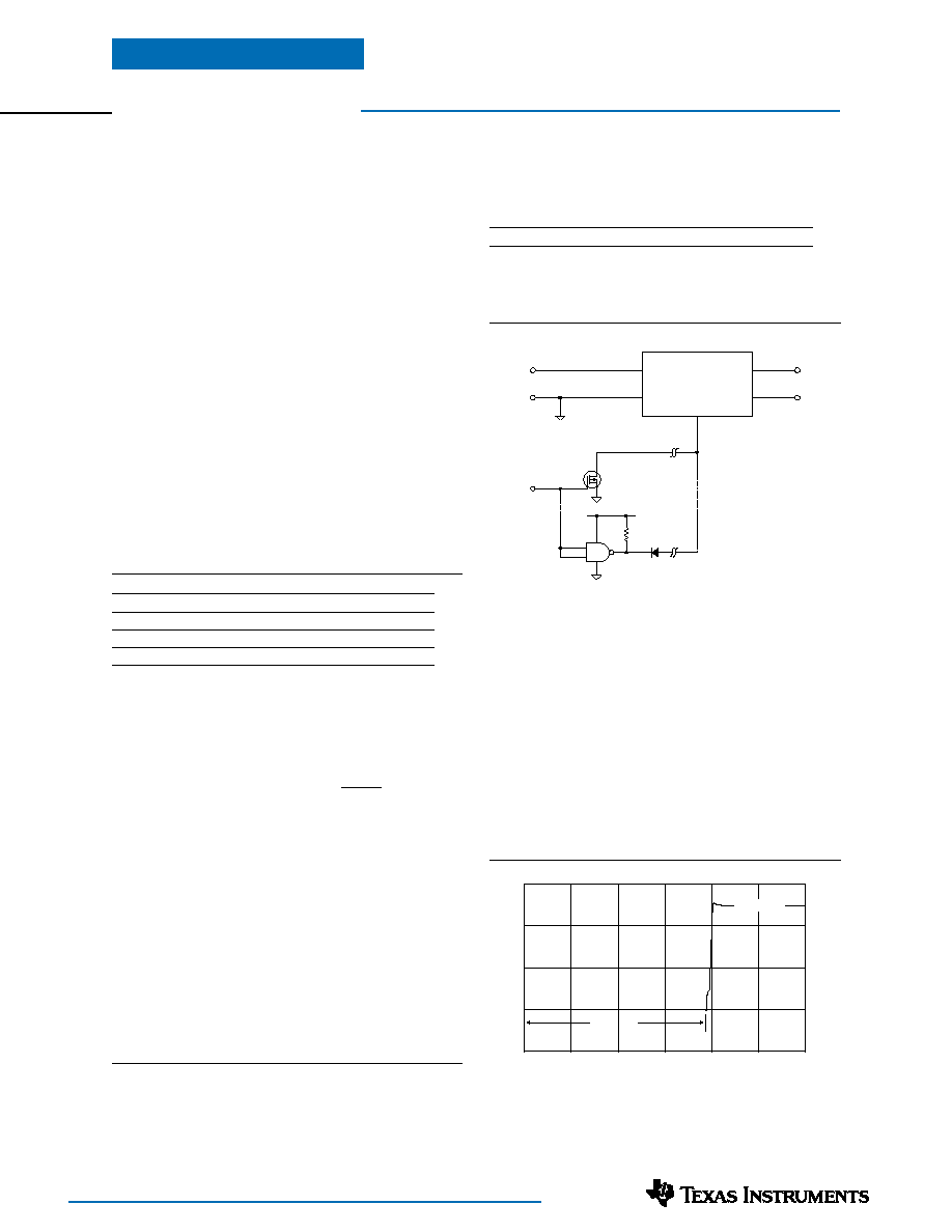
PT4210 Series
Using the Remote On/Off Function on the
PT4210 Isolated 7W DC/DC Converters
Applications requiring output voltage On/Off control, the
PT4210 DC/DC converter series incorporates a "Remote
On/Off" control (pin 11). This feature can be used when
there is a requirement for the module to be switched off
without removing the applied input source voltage.
The converter functions normally with Pin 11 open-circuit,
providing a regulated output voltage when a valid source
voltage is applied to +V
in
(pin 18), with respect to V
in
(pin 17). When a low-level
1
ground signal is applied to
pin 11, the converter output will be turned off.
Figure 1 shows an application schematic, which details
the typical use of the Remote On/Off function. Note the
discrete transistor (Q1). The control pin has its own
internal pull-up, and must be controlled with an open-
collector or open-drain device (See notes 2 & 3). Table 1
gives the input requirements.
When placed in the "Off" state, the standby current drawn
from the input source is typically reduced to less than 1mA.
Table 1; Remote On/Off Control Requirements
1
Parameter
Min
Typ
Max
Disable
-0.1V
--
1.0V
Enable
5.0V 3
--
Open-Circuit 2
Vo/c [Open-Circuit]
--
--
10V
Iin [pin 11 at Vin]
--
100µA
--
Notes:
1. The Remote On/Off control uses V
in
(pin 17) as its ground
reference. All voltages specified are with respect to V
in
.
2. Use an open-collector device (preferably a discrete
transistor) for the Remote On/Off input. Do not connect a
pull-up resistor directly to pin 11.
3. The Remote On/Off pin may be controlled with devices that have
a totem-pole output providing that a blocking diode is
used (See Figure 1). The blocking diode is required to
prevent current from being injected into On/Off control
pin. Note: For TTL devices a pull-up may be required on the
cathode side of the blocking diode. This is to guarantee a
minimum enable voltage at pin 11 (See Figure 1).
4. The PT4210 converters incorporate an "Under-Voltage
Lockout" (UVLO). The UVLO will keep the module off
when the input voltage to the converter is low, regardless of
the state of the Remote On/Off control. Table 2 gives the
UVLO input voltage thresholds.
Table 2; UVLO Thresholds
4
Figure 1
Turn-On Time:
In the circuit of Figure 1, turning Q
1
on applies a
low-voltage to pin 11 and disables the converter output.
Correspondingly, turning Q
1
off allows pin 11 to be pulled
high by an internal pull-up resistor. The converter produces a
regulated output voltage within 50ms. Although the rise-
time of the output is short (<1ms), the delay time will vary
depending upon the input voltage and the module's internal
timing. Figure 2 shows shows an example of the output
response for a PT4213 (5.0V), following the turn-off of
Q
1
at time t =0. The waveform was measured with a 48Vdc
input voltage, and 1.2Adc resistive load.
Figure 2
R1
10k
Q1
BSS138
+ V
o
-V
o
+ V
in
-V
in
Vdd
1 = O F F
Note 1
U1a
Note 1
Note 1
D1
1N4148
#
#
or similar low-leakage PIN diode
PT4210
+ V out
-Vout
+ Vin
-Vin
Remote
On/Off*
11
17
18
1
2
Series
V
in
Range
UVLO Threshold
PT4210
38 75V
36V ±2V
0
5
10
15
20
25
30
time (milli-secs)
V
O
(2V/Div)
delay time
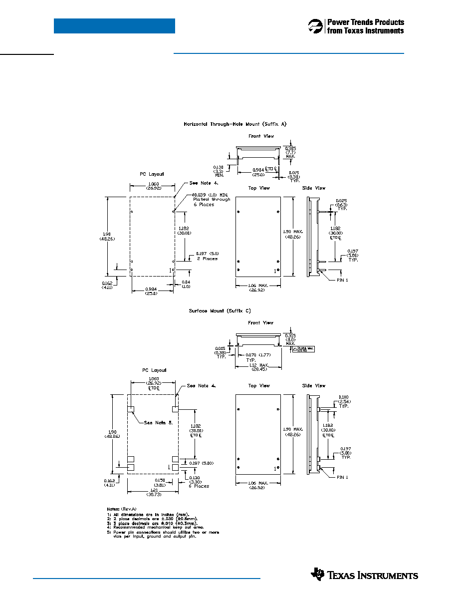
PACKAGE INFORMATION AND DIMENSIONS
For technical support and more information, see inside back cover or visit www.ti.com/powertrends
Package Style 910
Suffix A, C
(Revised 12/1/2000)

IMPORTANT NOTICE
Texas Instruments and its subsidiaries (TI) reserve the right to make changes to their products or to discontinue
any product or service without notice, and advise customers to obtain the latest version of relevant information
to verify, before placing orders, that information being relied on is current and complete. All products are sold
subject to the terms and conditions of sale supplied at the time of order acknowledgment, including those
pertaining to warranty, patent infringement, and limitation of liability.
TI warrants performance of its products to the specifications applicable at the time of sale in accordance with
TI's standard warranty. Testing and other quality control techniques are utilized to the extent TI deems necessary
to support this warranty. Specific testing of all parameters of each device is not necessarily performed, except
those mandated by government requirements.
Customers are responsible for their applications using TI components.
In order to minimize risks associated with the customer's applications, adequate design and operating
safeguards must be provided by the customer to minimize inherent or procedural hazards.
TI assumes no liability for applications assistance or customer product design. TI does not warrant or represent
that any license, either express or implied, is granted under any patent right, copyright, mask work right, or other
intellectual property right of TI covering or relating to any combination, machine, or process in which such
products or services might be or are used. TI's publication of information regarding any third party's products
or services does not constitute TI's approval, license, warranty or endorsement thereof.
Reproduction of information in TI data books or data sheets is permissible only if reproduction is without
alteration and is accompanied by all associated warranties, conditions, limitations and notices. Representation
or reproduction of this information with alteration voids all warranties provided for an associated TI product or
service, is an unfair and deceptive business practice, and TI is not responsible nor liable for any such use.
Resale of TI's products or services with
statements different from or beyond the parameters stated by TI for
that product or service voids all express and any implied warranties for the associated TI product or service,
is an unfair and deceptive business practice, and TI is not responsible nor liable for any such use.
Also see: Standard Terms and Conditions of Sale for Semiconductor Products. www.ti.com/sc/docs/stdterms.htm
Mailing Address:
Texas Instruments
Post Office Box 655303
Dallas, Texas 75265
Copyright
2001, Texas Instruments Incorporated