
www.ti.com
FEATURES
DESCRIPTION
APPLICATIONS
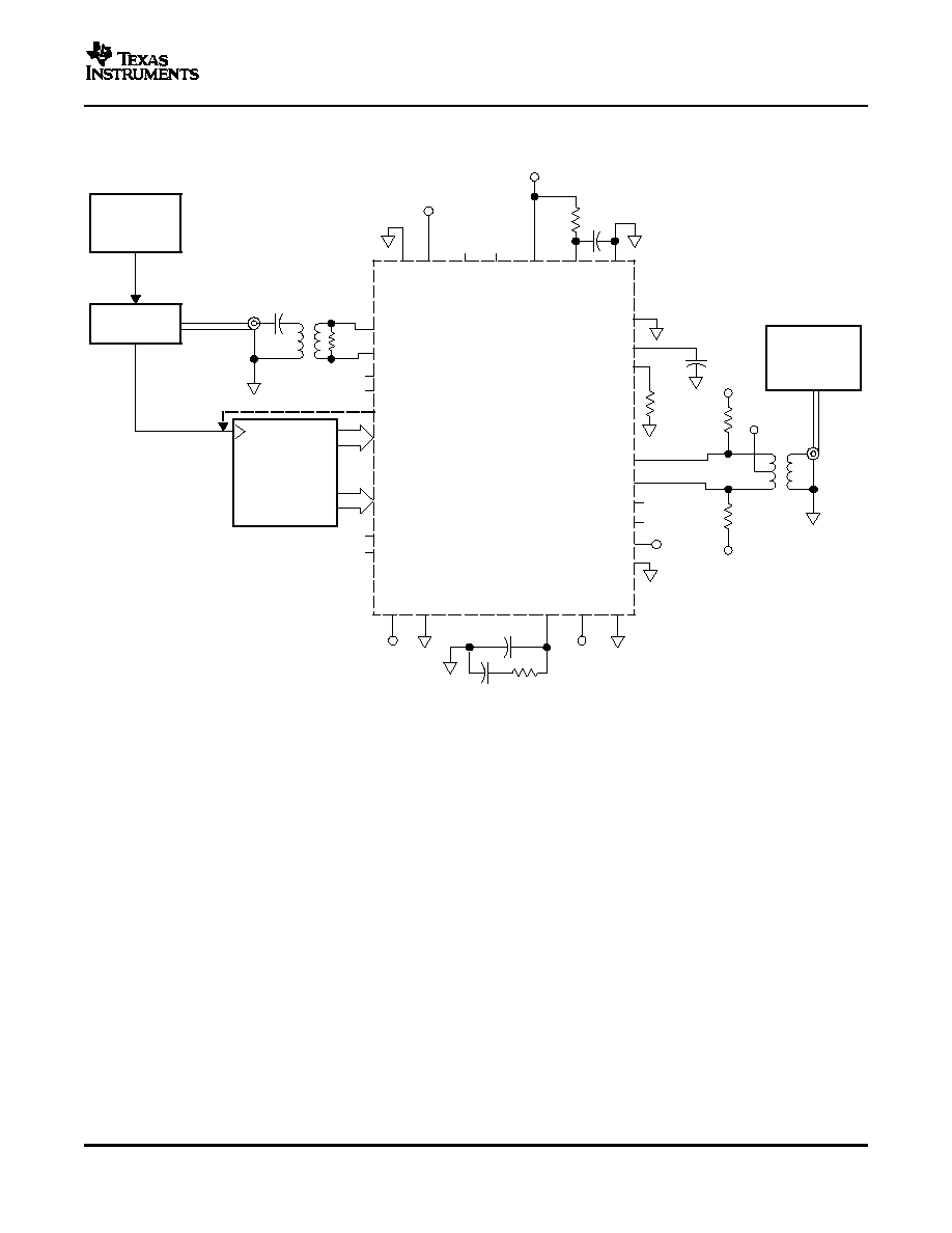
DAC5687
SLWS164B FEBRUARY 2005 REVISED JUNE 2005
16-BIT, 500 MSPS 2x-8x INTERPOLATING DUAL-CHANNEL
DIGITAL-TO-ANALOG CONVERTER (DAC)
·
500 MSPS
The DAC5687 is a dual-channel 16-bit high-speed
digital-to-analog converter (DAC) with integrated 2x,
·
Selectable 2x-8x Interpolation
4x, and 8x interpolation filters, a complex numerically
·
On-Chip PLL/VCO Clock Multiplier
controlled oscillator (NCO), on-board clock multiplier,
·
Full IQ Compensation Including Offset, Gain,
IQ compensation and on-chip voltage reference. The
and Phase
DAC5687 is pin compatible to the DAC5686, requir-
ing only changes in register settings for most appli-
·
Flexible Input Options:
cations, and offers additional features and superior
FIFO With Latch on External or Internal
linearity, noise, crosstalk, and PLL phase noise per-
Clock
formance.
Even/Odd Multiplexed Input
The DAC5687 has six signal processing blocks: two
Single Port Demultiplexed Input
interpolate by two digital filters, fine frequency mixer
·
Complex Mixer With 32-Bit NCO
with 32-bit NCO, a quadrature modulation compen-
sation block, another interpolate by two digital filter
·
Fixed Frequency Mixer With Fs/4 and Fs/2
and a coarse frequency mixer with Fs/2 or Fs/4. The
·
1.8-V or 3.3-V I/O Voltage
different modes of operation enable or bypass the
·
On-Chip 1.2-V Reference
signal processing blocks.
·
Differential Scalable Output: 2 mA to 20 mA
The coarse and fine mixers can be combined to span
·
Pin Compatible to DAC5686
a wider range of frequencies with fine resolution. The
DAC5687 allows both complex or real output. Com-
·
High Performance
bining the frequency upconversion and complex out-
81-dBc ACLR WCDMA TM1 at 30.72 MHz
put produces a Hilbert Transform pair that is output
72-dBc ACLR WCDMA TM1 at 153.6 MHz
from the two DACs. An external RF quadrature
modulator then performs the final single sideband
·
Package: 100-Pin HTQFP
up-conversion.
The IQ compensation feature allows optimization of
·
Cellular Base Transceiver Station Transmit
phase, gain and offset to maximize sideband rejection
Channel
and minimize LO feedthrough for an analog quadra-
ture modulator.
CDMA: W-CDMA, CDMA2000, TD-SCDMA
TDMA: GSM, IS-136, EDGE/UWC-136
The DAC5687 includes several input options: single
port interleaved data, even and odd multiplexing at
OFDM: 802.16
half rate, and an input FIFO with either external or
·
Cable Modem Termination System
internal clock to ease the input timing ambiguity when
the DAC5687 is clocked at the DAC output sample
rate.
ORDERING INFORMATION
T
A
Package Device
100 HTQFP
(1)
(P&P) PowerPADTM
Plastic Quad FlatPack
-40°C to 85°C
DAC5687IPZP
(1)
Thermal Pad Size: 6 mm
×
6 mm.
Please be aware that an important notice concerning availability, standard warranty, and use in critical applications of Texas
Instruments semiconductor products and disclaimers thereto appears at the end of this data sheet.
PRODUCTION DATA information is current as of publication date.
Copyright © 2005, Texas Instruments Incorporated
Products conform to specifications per the terms of the Texas
Instruments standard warranty. Production processing does not
necessarily include testing of all parameters.

www.ti.com
100-Pin HTQFP
CLKVDD
CLKGND
LPF
PLLGND PLLVDD
PHSTR
SLEEP
DVDD
DGND
EXTIO
EXTLO
BIASJ
IOUTA1
IOUTA2
IOUTB1
IOUTB2
IOGND
IOVDD
1.2-V
Reference
SDIO SDO SDENB SCLK
AVDD
AGND
CLK2
CLK2C
CLK1
CLK1C
PLLLOCK
DA[15:0]
DB[15:0]
TXENABLE
RESETB
Internal Clock Generation
and
2x-8x PLL Clock Multiplier
2x-8x
f
data
Input FIFO/
Reorder/
Mux/Demux
FIR1
FIR2
FIR3
FIR4
x2
x2
x2
x2
x2
x2
Fine Mixer
Coarse Mixer:
fs/2 or fs/4
x:
sin(x)
x:
sin(x)
A
Offset
A gain
16-bit DAC
SIF
NCO
B
Offset
B gain
cos
sin
16-bit DAC
Quardrature Mod
Correction (QMC)
QFLAG
DAC5687
SLWS164B FEBRUARY 2005 REVISED JUNE 2005
These devices have limited built-in ESD protection. The leads should be shorted together or the device
placed in conductive foam during storage or handling to prevent electrostatic damage to the MOS gates.
FUNCTIONAL BLOCK DIAGRAM
2

www.ti.com
PINOUT
1
2
3
4
5
6
7
8
9
10
11
12
13
14
15
16
17
18
19
20
75
74
73
72
71
70
69
68
67
66
65
64
63
62
61
60
59
58
57
56
1
0
0
9
9
9
8
9
7
9
6
9
5
9
4
9
3
9
2
9
1
9
0
8
9
8
8
8
7
8
6
8
5
8
4
8
3
8
2
2
6
2
7
2
8
2
9
3
0
3
1
3
2
3
3
3
4
3
5
3
6
3
7
3
8
3
9
4
0
21
22
23
24
25
4
1
4
2
4
3
4
4
4
5
4
6
4
7
4
8
4
9
5
0
55
54
53
52
51
8
1
8
0
7
9
7
8
7
7
7
6
DAC5687
Top View 100 HTQFP
D
V
D
D
D
G
N
D
QFLAG
T
E
S
T
M
O
D
E
S
L
E
E
P
R
E
S
E
T
B
P
H
S
T
R
D
G
N
D
D
B
1
5
(
M
S
B
)
D
B
1
4
D
B
1
3
D
V
D
D
D
G
N
D
D
B
1
2
D
B
1
1
D
B
1
0
D
B
9
D
B
8
D
V
D
D
D
G
N
D
I
O
V
D
D
I
O
G
N
D
D
B
7
D
B
6
D
B
5
DA4
DA3
DA2
DA1
DA0 (LSB)
DVDD
DGND
CLKGND
CLK1
CLK1C
CLKVDD
CLK2
CLK2C
CLKGND
PLLGND
LPF
PLLVDD
DVDD
DGND
PLLLOCK
DB0 (LSB)
DB1
DB2
DB3
DB4
D
V
D
D
D
G
N
D
S
D
E
N
B
S
C
L
K
S
D
I
O
S
D
O
D
V
D
D
T
X
E
N
A
B
L
E
D
A
1
5
(
M
S
B
)
D
A
1
4
D
A
1
3
D
V
D
D
D
G
N
D
D
A
1
2
D
A
1
1
D
A
1
0
D
A
9
D
A
8
D
V
D
D
D
G
N
D
I
O
V
D
D
I
O
G
N
D
D
A
7
D
A
6
D
A
5
AGND
AVDD
AVDD
AGND
IOUTA1
IOUTA2
AGND
AVDD
AGND
AVDD
EXTLO
AVDD
BIASJ
AGND
EXTIO
AVDD
AGND
AVDD
AGND
IOUTB2
IOUTB1
AGND
AVDD
AVDD
AGND
DAC5687
SLWS164B FEBRUARY 2005 REVISED JUNE 2005
TERMINAL FUNCTIONS
TERMINAL
I/O
DESCRIPTION
NAME
NO.
1, 4, 7, 9, 12,
AGND
I
Analog ground return
17, 19, 22, 25
2, 3, 8, 10, 14,
AVDD
I
Analog supply voltage
16, 18, 23, 24
BIASJ
13
O
Full-scale output current bias
3

www.ti.com
DAC5687
SLWS164B FEBRUARY 2005 REVISED JUNE 2005
TERMINAL FUNCTIONS (continued)
TERMINAL
I/O
DESCRIPTION
NAME
NO.
In PLL clock mode and dual clock modes, provides data input rate clock. In external clock mode,
CLK1
59
I
provides optional input data rate clock to FIFO latch. When the FIFO is disabled, CLK1 is not used
and can be left unconnected.
CLK1C
60
I
Complementary input of CLK1.
External and dual clock mode clock input. In PLL mode, CLK2 is unused and can be left
CLK2
62
I
unconnected.
CLK2C
63
I
Complementary of CLK2. In PLL mode, CLK2C is unused and can be left unconnected.
CLKGND
58, 64
I
Ground return for internal clock buffer
CLKVDD
61
I
Internal clock buffer supply voltage
34-36, 39-43,
A-Channel Data bits 0 through 15. DA15 is most significant data bit (MSB). DA0 is least significant
DA[15..0]
I
48-55
data bit (LSB). Order can be reversed by register change.
71-78, 83-87,
B-Channel Data bits 0 through 15. DB15 is most significant data bit (MSB). DB0 is least significant
DB[0..15]
I
90-92
data bit (LSB). Order can be reversed by register change.
27, 38, 45, 57,
DGND
69, 81, 88, 93,
I
Digital ground return
99
26, 32, 37, 44,
DVDD
56, 68, 82, 89,
I
Digital supply voltage
100
Used as external reference input when internal reference is disabled (i.e., EXTLO connected to
EXTIO
11
I/O
AVDD). Used as internal reference output when EXTLO = AGND, requires a 0.1-µF decoupling
capacitor to AGND when used as reference output
Internal/external reference select. Internal reference selected when tied to AGND, external
EXTLO
15
I/O
reference selected when tied to AVDD. Output only when ATEST is not zero (register 0x1B bits 7
to 3).
IOUTA1
21
O
A-Channel DAC current output. Full scale when all input bits are set 1
IOUTA2
20
O
A-Channel DAC complementary current output. Full scale when all input bits are 0
IOUTB1
5
O
B-Channel DAC current output. Full scale when all input bits are set 1
IOUTB2
6
O
B-Channel DAC complementary current output. Full scale when all input bits are 0
IOGND
47, 79
I
Digital I/O ground return
IOVDD
46, 80
I
Digital I/O supply voltage
LPF
66
I
PLL loop filter connection
Synchronization input signal that can be used to initialize the NCO, course mixer, internal clock
PHSTR
94
I
divider, and/or FIFO circuits.
PLLGND
65
I
Ground return for internal PLL
PLLVDD
67
I
PLL supply voltage. When PLLVDD is 0 V, the PLL is disabled.
In PLL mode, provides PLL lock status bit or internal clock signal. PLL is locked to input clock
PLLLOCK
70
O
when high. In external clock mode, provides input rate clock.
When qflag register is 1, the QFLAG pin is used by the user during interleaved data input mode to
QFLAG
98
I
identify the B sample. High QFLAG indicates B sample. Must be repeated every B sample.
RESETB
95
I
Resets the chip when low. Internal pull-up
SCLK
29
I
Serial interface clock
SDENB
28
I
Active low serial data enable, always an input to the DAC5687
Bidirectional serial data in 3-pin interface mode, input only in 4 pin interface mode. Three-pin mode
SDIO
30
I/O
is the default after chip reset.
Serial interface data, uni-directional data output, if SDIO is an input. SDO is 3-stated when the
SDO
31
O
3-pin interface mode is selected (register 0x08 bit 1).
SLEEP
96
I
Asynchronous hardware power down input. Active High. Internal pull down.
4

www.ti.com
ABSOLUTE MAXIMUM RATINGS
THERMAL CHARACTERISTICS
(1)
DAC5687
SLWS164B FEBRUARY 2005 REVISED JUNE 2005
TERMINAL FUNCTIONS (continued)
TERMINAL
I/O
DESCRIPTION
NAME
NO.
TXENABLE has two purposes. In all modes, TXENABLE must be high for the DATA to the DAC to
be enabled. When TXENABLE is low, the digital logic section is forced to all 0, and any input data
presented to DA[15:0] and DB[15:0] is ignored. In interleaved data mode, when the qflag register
TXENABLE
33
I
bit is cleared, TXENABLE is used to synchronizes the data to channels A and B. The first data
after the rising edge of TXENABLE is treated as A data, while the next data is treated as B data,
and so on.
TESTMODE
97
I
TESTMODE is DGND for the user
over operating free-air temperature range (unless otherwise noted)
(1)
UNIT
AVDD
(2)
0.5 V to 4 V
DVDD
(3)
0.5 V to 2.3 V
Supply voltage range
CLKVDD
(2)
0.5 V to 4 V
IOVDD
(2)
0.5 V to 4 V
PLLVDD
(2)
0.5 V to 4 V
Voltage between AGND, DGND, CLKGND, PLLGND, and IOGND
0.5 V to 0.5 V
AVDD to DVDD
0.5 V to 2.6 V
DA[15..0]
(4)
0.5 V to IOVDD + 0.5 V
DB[15..0]
(4)
0.5 V to IOVDD + 0.5 V
SLEEP
(4)
0.5 V to IOVDD + 0.5 V
CLK1/2, CLK1/2C
(3)
0.5 V to CLKVDD + 0.5 V
Supply voltage range
RESETB
(4)
0.5 V to IOVDD + 0.5 V
LPF
(4)
0.5 V to PLLVDD + 0.5 V
IOUT1, IOUT2
(2)
1.0 V to AVDD + 0.5 V
EXTIO, BIASJ
(2)
0.5 V to AVDD + 0.5 V
EXTLO
(2)
0.5 V to IAVDD + 0.5 V
Peak input current (any input)
20 mA
Peak total input current (all inputs)
30 mA
T
A
Operating free-air temperature range (DAC5687I)
40°C to 85°C
T
stg
Storage temperature range
65°C to 150°C
Lead temperature 1,6 mm (1/16 inch) from the case for 10 seconds
260°C
(1)
Stresses beyond those listed under absolute maximum ratings may cause permanent damage to the device. These are stress ratings
only, and functional operation of these or any other conditions beyond those indicated under recommended operating conditions is not
implied. Exposure to absolute-maximum-rated conditions for extended periods may affect device reliability.
(2)
Measured with respect to AGND.
(3)
Measured with respect to DGND.
(4)
Measured with respect to IOGND.
over operating free-air temperature range (unless otherwise noted)
Thermal Conductivity
100 HTQFP
UNIT
T
J
Junction temperature
(2)
105
°C
Theta junction-to-ambient (still air)
19.88
°C/W
JA
Theta junction-to-ambient (150 lfm)
14.37
°C/W
JC
Theta junction-to-case
0.12
°C/W
(1)
Air flow or heat sinking reduces
JA
and is highly recommended.
(2)
Air flow or heat sinking required for sustained operation at 85
°
C and maximum operating conditions to maintain junction temperature.
5

www.ti.com
ELECTRICAL CHARACTERISTICS
DAC5687
SLWS164B FEBRUARY 2005 REVISED JUNE 2005
over recommended operating free-air temperature range, AVDD = 3.3 V, CLKVDD = 3.3 V, PLLVDD = 3.3 V, IOVDD = 3.3 V,
DVDD = 1.8 V, IOUT
FS
= 19.2 mA (unless otherwise noted)
DC SPECIFICATIONS
PARAMETER
TEST CONDITIONS
MIN
TYP
MAX
UNIT
RESOLUTION
16
Bits
DC ACCURACY
(1)
1 LSB = IOUT
FS
/2
16
INL
Integral nonlinearity
±4
LSB
T
MIN
to T
MAX
DNL
Differential nonlinearity
±4
LSB
ANALOG OUTPUT
Coarse gain linearity
±0.04
LSB
Worst case error from ideal linearity
Fine gain linearity
±3
LSB
Offset error
Mid code offset
0.01
%FSR
Without internal reference
1
%FSR
Gain error
With internal reference
0.7
%FSR
With internal reference, dual DAC, and SSB
Gain mismatch
-2
2
%FSR
mode
Minimum full-scale output current
(2)
2
mA
Maximum full-scale output current
(2)
20
mA
AVDD
AVDD +
Output compliance range
(3)
IOUT
FS
= 20 mA
V
0.5 V
0.5 V
Output resistance
300
k
Output capacitance
5
pF
REFERENCE OUTPUT
Reference voltage
1.14
1.2
1.26
V
Reference output current
(4)
100
nA
REFERENCE INPUT
V
EXTIO
Input voltage range
0.1
1.25
V
Input resistance
1
M
Small signal bandwidth
1.4
MHz
Input capacitance
100
pF
TEMPERATURE COEFFICIENTS
ppm of
Offset drift
±1
FSR/°C
Without internal reference
±15
ppm of
Gain drift
FSR/°C
With internal reference
±30
ppm of
Reference voltage drift
±8
FSR/°C
POWER SUPPLY
AVDD
Analog supply voltage
3
3.3
3.6
V
DVDD
Digital supply voltage
1.71
1.8
2.15
V
CLKVDD
Clock supply voltage
3
3.3
3.6
V
IOVDD
I/O supply voltage
1.71
3.6
V
PLLVDD
PLL supply voltage
3
3.3
3.6
V
(1)
Measured differential across IOUTA1 and IOUTA2 or IOUTB1 and IOUTB2 with 25
each to AVDD.
(2)
Nominal full-scale current, IOUT
FS
, equals 32X the IBIAS current.
(3)
The lower limit of the output compliance is determined by the CMOS process. Exceeding this limit may result in transistor breakdown,
resulting in reduced reliability of the DAC5687 device. The upper limit of the output compliance is determined by the load resistors and
full-scale output current. Exceeding the upper limit adversely affects distortion performance and integral nonlinearity.
(4)
Use an external buffer amplifier with high impedance input to drive any external load.
6

www.ti.com
DAC5687
SLWS164B FEBRUARY 2005 REVISED JUNE 2005
ELECTRICAL CHARACTERISTICS (continued)
over recommended operating free-air temperature range, AVDD = 3.3 V, CLKVDD = 3.3 V, PLLVDD = 3.3 V, IOVDD = 3.3 V,
DVDD = 1.8 V, IOUT
FS
= 19.2 mA (unless otherwise noted)
DC SPECIFICATIONS
PARAMETER
TEST CONDITIONS
MIN
TYP
MAX
UNIT
Mode 5
(5)
41
mA
I
AVDD
Analog supply current
Mode 6
(5)
80
mA
I
DVDD
Digital supply current
(5)
Mode 6
(5)
587
mA
I
CLKVDD
Clock supply current
(5)
Mode 6
(5)
5
mA
I
PLLVDD
PLL supply current
(5)
Mode 6
(5)
20
mA
I
IOVDD
IO supply current
(5)
Mode 6
(5)
2
mA
I
AVDD
Sleep mode AVDD supply current
Sleep mode (Sleep pin high) CLK2 = 500 MHz
1
mA
I
DVDD
Sleep mode DVDD supply current
Sleep mode (Sleep pin high) CLK2 = 500 MHz
2
mA
I
CLKVDD
Sleep mode CLKVDD supply current Sleep mode (Sleep pin high) CLK2 = 500 MHz
0.25
mA
I
PLLVDD
Sleep mode PLLVDD supply current
Sleep mode (Sleep pin high) CLK2 = 500 MHz
0.6
mA
I
IOVDD
Sleep mode IOVDD supply current
Sleep mode (Sleep pin high) CLK2 = 500 MHz
0.6
mA
Mode 1
(5)
AVDD = 3.3 V, DVDD = 1.8 V
750
Mode 2
(5)
AVDD = 3.3 V, DVDD = 1.8 V
910
Mode 3
(5)
AVDD = 3.3 V, DVDD = 1.8 V
760
Mode 4
(5)
AVDD = 3.3 V, DVDD = 1.8 V
1250
P
D
Power dissipation
mW
Mode 5
(5)
AVDD = 3.3 V, DVDD = 1.8 V
1250
Mode 6
(5)
AVDD = 3.3 V, DVDD = 1.8 V
1410
Mode 7
(5)
AVDD = 3.3 V, DVDD = 1.8 V
1400
1750
Sleep mode (Sleep pin high) CLK2 = 500 MHz
11
20
APSRR
-0.2
0.2
%FSR/V
Power supply rejection ratio
DPSRR
-0.2
0.2
%FSR/V
(5)
MODE 1 MODE 7:
a. Mode 1: X2, PLL off, CLK2 = 320 MHz, DACA and DACB on, IF = 5 MHz
b. Mode 2: X4 QMC, PLL on, CLK1 = 125 MHz, DACA and DACB on, IF = 5 MHz
c. Mode 3: X4 CMIX, PLL off, CLK2 = 500 MHz, DACA off and DACB on, IF = 150 MHz
d. Mode 4: X4L FMIX CMIX, PLL off, CLK2 = 500 MHz, DACA off and DACB on, IF = 150 MHz
e. Mode 5: X4L FMIX CMIX, PLL on, CLK1 = 125 MHz, DACA off and DACB on, IF = 150 MHz
f. Mode 6: X4L FMIX CMIX, PLL on, CLK1 = 125 MHz, DACA on and DACB on, IF = 150 MHz
g. Mode 7: X8 FMIX CMIX, PLL on, CLK1 = 62.5 MHz, DACA and DACB on, IF = 150 MHz
7

www.ti.com
ELECTRICAL CHARACTERISTICS
(1)
DAC5687
SLWS164B FEBRUARY 2005 REVISED JUNE 2005
over recommended operating free-air temperature range, AVDD = 3.3 V, CLKVDD = 3.3 V, PLLVDD = 0 V (= 3.3 V for PLL
Clock Mode), IOVDD = 3.3 V, DVDD = 1.8 V, IOUT
FS
= 19.2 mA, External Clock Mode, 4:1 transformer output termination,
50-
doubly terminated load (unless otherwise noted)
AC SPECIFICATIONS
PARAMETER
TEST CONDITIONS
MIN
TYP
MAX
UNIT
ANALOG OUTPUT
f
CLK
Maximum output update rate
500
MSPS
t
s(DAC)
Output settling time to 0.1%
Transition: Code 0x0000 to 0xFFFF
10.4
ns
t
pd
Output propagation delay
3
ns
t
r(IOUT)
Output rise time 10% to 90%
2
ns
t
f(IOUT)
Output fall time 90% to 10%
2
ns
AC PERFORMANCE
X2, PLL off, CLK2 = 250 MHz, DAC A and DAC B on,
78
IF = 5.1 MHz, First Nyquist Zone < f
DATA
/2
X4, PLL off, CLK2 = 500 MHz, DAC A and DAC B on,
77
SFDR
Spurious free dynamic range
(2)
IF = 5.1 MHz, First Nyquist Zone < f
DATA
/2
dBc
X4, CLK2 = 500 MHz, DAC A and DAC B on,
IF = 20.1 MHz, PLL on for Min, PLL off for TYP,
68
(3)
76
First Nyquist Zone < f
DATA
/2
X4, PLL off, CLK2 = 500 MSPS, DAC A and DAC B on,
73
Single tone, 0 dBFS, IF = 20.1 MHz
X4 CMIX, PLL off, CLK2 = 500 MSPS, DAC A and DAC B
65
on, IF = 70.1 MHz
X4 CMIX, PLL off, CLK2 = 500 MSPS, DAC A and DAC B
57
SNR
Signal-to-noise ratio
on, Single tone, 0 dBFS, IF = 150.1 MHz
dBc
X4 FMIX CMIX, PLL off, CLK2 = 500 MSPS, DAC A and
54
DAC B on, Single tone, 0 dBFS, IF = 180.1 MHz
X4, PLL off, CLK2 = 500 MSPS, DAC A and DAC B
on,Four tone, each -12 dBFS, IF = 24.7, 24.9, 25.1, 25.3
73
MHz
X4, PLL off, CLK2 = 500 MSPS, DAC A and DAC B on,
79
IF = 20.1 and 21.1 MHz
X4 CMIX, PLL off, CLK2 = 500 MSPS, DAC A and DAC B
73
Third-order two-tone
on, IF = 70.1 and 71.1 MHz
IMD3
intermodulation (each tone at
dBc
X4 CMIX, PLL off, CLK2 = 500 MSPS, DAC A and DAC B
6 dBFS)
68
on, IF= 150.1 and 151.1 MHz
X4 FMIX CMIX, PLL off, CLK2 = 500 MSPS, DAC A and
67
DAC B on, IF = 180.1 and 181.1 MHz
Four-tone Intermodulation to
X4 CMIX, CLK2 = 500 MHz f
OUT
= 149.2, 149.6, 150.4,
IMD
Nyquist (each tone at 12
66
dBc
and 150.8 MHz
dBFS)
(1)
Measured single ended into 50-
load.
(2)
See the Non-Harmonic Clock Related Spurious Signals section for information on spurious products out of band (< f
DATA
/2).
(3)
1:1 transformer output termination.
8

www.ti.com
ELECTRICAL CHARACTERISTICS (DIGITAL SPECIFICATIONS)
DAC5687
SLWS164B FEBRUARY 2005 REVISED JUNE 2005
ELECTRICAL CHARACTERISTICS (continued)
over recommended operating free-air temperature range, AVDD = 3.3 V, CLKVDD = 3.3 V, PLLVDD = 0 V (= 3.3 V for PLL
Clock Mode), IOVDD = 3.3 V, DVDD = 1.8 V, IOUT
FS
= 19.2 mA, External Clock Mode, 4:1 transformer output termination,
50-
doubly terminated load (unless otherwise noted)
AC SPECIFICATIONS
PARAMETER
TEST CONDITIONS
MIN
TYP
MAX
UNIT
Single carrier, baseband, X4, PLL Clock Mode,
78.4
CLK1 = 122.88 MHz
Single carrier, baseband, X4, PLL Clock Mode,
78.5
CLK2 = 491.52 MHz
Single carrier, IF = 153.6 MHz, X4 CMIX, External Clock
70.9
Mode, CLK2 = 491.52 MHz
Two carrier, IF = 153.6 MHz, X4 CMIX, External Clock
67.8
Mode, CLK2 = 491.52 MHz
Four carrier, baseband, X4, External Clock Mode,
76.1
CLK2 = 491.52 MHz
ACLR
(4)
Adjacent channel leakage ratio
dBc
Four carrier, IF = 92.16 MHz, X4L, External Clock Mode,
66.8
CLK2 = 491.52 MHz
Single carrier, IF = 153.6 MHz, X4 CMIX, External Clock
72.2
Mode, CLK2 = 491.52 MHz, DVDD = 2.1 V
Two carrier, IF = 153.6 MHz, X4 CMIX, External Clock
69.3
Mode, CLK2 = 491.52 MHz, DVDD = 2.1 V
Four carrier, baseband, X4, External Clock Mode,
68.5
CLK2 = 491.52 MHz, DVDD = 2.1 V
Four carrier, IF = 92.16 MHz, X4L, External Clock Mode,
66.3
CLK2 = 491.52 MHz, DVDD = 2.1 V
50-MHz offset, 1-MHz BW, Single carrier, baseband,
92
X4, External Clock Mode, CLK1 = 122.88 MHz
50-MHz offset, 1-MHz BW, Four carrier, baseband,
81
X4, External Clock Mode, CLK1 = 122.88 MHz
Noise Floor
dBc
50-MHz offset, 1-MHz BW, Single carrier, baseband,
88
X4, PLL Clock Mode, CLK2 = 491.52 MHz
50-MHz offset, 1-MHz BW, Four carrier, baseband,
81
X4, PLL Clock Mode, CLK2 = 491.52 MHz
(4)
W-CDMA with 3.84 MHz BW, 5-MHz spacing, centered at IF. TESTMODEL 1, 10 ms
over recommended operating free-air temperature range, AVDD = 3.3 V, CLKVDD = 3.3 V, PLLVDD = 3.3 V, IOVDD = 3.3 V,
DVDD = 1.8 V, IOUT
FS
= 19.2 mA (unless otherwise noted)
DIGITAL SPECIFICATIONS
PARAMETER
TEST CONDITIONS
MIN
TYP
MAX
UNIT
CMOS INTERFACE
V
IH
High-level input voltage
2
3
V
V
IL
Low-level input voltage
0
0
0.8
V
I
IH
High-level input current
40
40
µA
I
IL
Low-level input current
40
40
µA
Input capacitance
5
pF
IOVDD
I
load
= 100 µA
V
0.2
V
OH
PLLLOCK, SDO, SDIO
0.8 x
I
load
= 8 mA
V
IOVDD
I
load
= 100 µA
0.2
V
V
OL
PLLLOCK, SDO, SDIO
0.22 x
I
load
= 8 mA
V
IOVDD
External or dual-clock modes
16
250
Input data rate
MSPS
PLL clock mode
16
160
9

www.ti.com
1
2F
CLK2
*
0.5 ns
DAC5687
SLWS164B FEBRUARY 2005 REVISED JUNE 2005
ELECTRICAL CHARACTERISTICS (DIGITAL SPECIFICATIONS) (continued)
over recommended operating free-air temperature range, AVDD = 3.3 V, CLKVDD = 3.3 V, PLLVDD = 3.3 V, IOVDD = 3.3 V,
DVDD = 1.8 V, IOUT
FS
= 19.2 mA (unless otherwise noted)
DIGITAL SPECIFICATIONS
PARAMETER
TEST CONDITIONS
MIN
TYP
MAX
UNIT
PLL
At 600-kHz offset, measured at DAC output,
25 MHz 0-dBFS tone, F
DATA
= 125 MSPS,
133
dBc/Hz
4x interpolation, pll_freq = 1, pll_kv = 0
Phase noise
At 6-MHz offset, measured at DAC output,
25 MHz 0-dBFS tone, 125 MSPS,
148.5
dBc/Hz
4x interpolation, pll_freq = 1, pll_kv = 0
pll_freq = 0, pll_kv = 0
370
pll_freq = 0, pll_kv = 1
480
VCO maximum frequency
MHz
pll_freq = 1, pll_kv = 0
495
pll_freq = 1, pll_kv = 1
520
pll_freq = 0, pll_kv = 0
225
pll_freq = 0, pll_kv = 1
200
VCO minimum frequency
MHz
pll_freq = 1, pll_kv = 0
480
pll_freq = 1, pll_kv = 1
480
NCO and QMC BLOCKS
QMC clock rate
320
MHz
NCO clock rate
320
MHz
SERIAL PORT TIMING
t
s(SDENB)
Setup time, SDENB to rising edge of SCLK
20
ns
Setup time, SDIO valid to rising edge of
t
s(SDIO)
10
ns
SCLK
Hold time, SDIO valid to rising edge of
t
h(SDIO)
5
ns
SCLK
t
SCLK
Period of SCLK
100
ns
t
SCLKH
High time of SCLK
40
ns
t
SCLK
Low time of SCLK
40
ns
t
d(Data)
Data output delay after falling edge of SCLK
10
ns
CLOCK INPUT (CLK1/CLK1C, CLK2/CLK2C)
Duty cycle
40%
60%
Differential voltage
0.4
1
V
TIMING PARALLEL DATA INPUT: CLK1 LATCHING MODES
(PLL Mode
Figure 45
, Dual Clock Mode FIFO Disabled See
Figure 47
, Dual Clock Mode With FIFO Enabled See
Figure 48
)
Setup time, DATA valid to rising edge of
t
s(DATA)
0.5
ns
CLK1
Hold time, DATA valid after rising edge of
t
h(DATA)
1.5
ns
CLK1
Maximum offset between CLK1 and CLK2
t_align
rising edges Dual Clock Mode with FIFO
ns
disabled
Timing Parallel Data Input (External Clock Mode, Latch on PLLLock Rising Edge, CLK2 Clock Input, See
Figure 43
)
Setup time, DATA valid to rising edge of
t
s(DATA)
72-
load on PLLLOCK
0.5
ns
PLLLOCK
Hold time, DATA valid after rising edge of
t
h(DATA)
72-
load on PLLLOCK
1.5
ns
PLLLOCK
Delay from CLK2 rising edge to PLLLOCK
72-
load on PLLLOCK. Note that PLLLOCK
t
delay(Plllock)
4.5
ns
rising edge
delay increases with a lower impedance load.
Timing Parallel Data Input (External Clock Mode, Latch on PLLLock Falling Edge, CLK2 Clock Input, See
Figure 44
)
Setup time, DATA valid to falling edge of
t
s(DATA)
High impedance load on PLLLOCK
0.5
ns
PLLLOCK
Hold time, DATA valid after falling edge of
t
h(DATA)
High impedance load on PLLLOCK
1.5
ns
PLLLOCK
10

www.ti.com
Typical Characteristics
1
Code
-8
-6
-4
-2
0
2
4
6
8
0
10000 20000 30000 40000 50000 60000 70000
Error - LSB
G001
Code
-6
-4
-2
0
2
4
6
0
10000 20000 30000 40000 50000 60000 70000
Error - LSB
G002
f - Frequency - MHz
-90
-80
-70
-60
-50
-40
-30
-20
-10
0
10
0
50
100
150
200
250
P - Power - dBm
G003
f
data
= 125 MSPS
f
in
= 20 MHz Real
IF = 20 MHz
y
4 Interpolation
PLL Off
f - Frequency - MHz
-90
-80
-70
-60
-50
-40
-30
-20
-10
0
10
0
50
100
150
200
250
P - Power - dBm
G004
f
data
= 125 MSPS
f
in
= -30 MHz Complex
IF = 95 MHz
y
4L Interpolation
CMIX
PLL Off
DAC5687
SLWS164B FEBRUARY 2005 REVISED JUNE 2005
ELECTRICAL CHARACTERISTICS (DIGITAL SPECIFICATIONS) (continued)
over recommended operating free-air temperature range, AVDD = 3.3 V, CLKVDD = 3.3 V, PLLVDD = 3.3 V, IOVDD = 3.3 V,
DVDD = 1.8 V, IOUT
FS
= 19.2 mA (unless otherwise noted)
DIGITAL SPECIFICATIONS
PARAMETER
TEST CONDITIONS
MIN
TYP
MAX
UNIT
High impedance load on PLLLOCK. Note that
Delay from CLK2 rising edge to PLLLOCK
t
delay(Plllock)
PLLLOCK delay increases with a lower im-
4.5
ns
rising edge
pedance load.
Figure 1. Integral Nonlinearity
Figure 2. Differential Nonlinearity
Figure 3. Single Tone Spectral Plot
Figure 4. Single Tone Spectral Plot
11

www.ti.com
f - Frequency - MHz
-90
-80
-70
-60
-50
-40
-30
-20
-10
0
10
0
50
100
150
200
250
f
data
= 125 MSPS
f
in
= 30 MHz Real
IF = 155 MHz
y
4L Interpolation
HP/HP
PLL Off
P - Power - dBm
G005
IF - Intermediate Frequency - MHz
60
65
70
75
80
85
90
95
100
5
10
15
20
25
30
35
f
data
= 125 MSPS
y
4 Interpolation
PLL Off
SFDR - Spurious-Free Dynamic Range - dBc
G006
0 dBFS
-6 dBFS
-12 dBFS
IF - Intermediate Frequency - MHz
40
45
50
55
60
65
70
75
80
85
90
0
50
100
150
200
250
f
data
= 125 MSPS
y
4 Interpolation
PLL Off
SFDR - Spurious-Free Dynamic Range - dBc
G007
0 dBFS
IF - Intermediate Frequency - MHz
50
55
60
65
70
75
80
85
90
95
100
0
50
100
150
200
250
f
data
= 125 MSPS
y
4L Interpolation
PLL Off
f
out
= IF
+
0.5 MHz
IMD3 - dBc
G008
0 dBFS
DAC5687
SLWS164B FEBRUARY 2005 REVISED JUNE 2005
Typical Characteristics (continued)
Figure 5. Single Tone Spectral Plot
Figure 6. In-Band SFDR vs Intermediate Frequency
Figure 7. Out-of-Band SFDR vs Intermediate Frequency
Figure 8. Two Tone IMD vs Intermediate Frequency
12

www.ti.com
Amplitude - dBFS
40
45
50
55
60
65
70
75
80
85
90
-35
-30
-25
-20
-15
-10
-5
0
IMD3 - dBC
G009
f
data
= 125 MSPS
f
in
= -30 MHz
+
0.5 MHz Complex
IF = 95 MHz
y
4L Interpolation
CMIX
PLL Off
f - Frequency - MHz
-100
-90
-80
-70
-60
-50
-40
-30
-20
-10
0
10
15
20
25
30
f
data
= 125 MSPS
f
in
= 20 MHz
+
0.5 MHz Real
IF = 20 MHz
y
4 Interpolation
PLL Off
P - Power - dBm
G010
f - Frequency - MHz
-100
-90
-80
-70
-60
-50
-40
-30
-20
-10
0
85
90
95
100
105
f
data
= 125 MSPS
f
in
= -30 MHz
+
0.5 MHz Complex
IF = 95 MHz
y
4L Interpolation
CMIX
PLL Off
P - Power - dBm
G011
IF - Intermediate Frequency - MHz
50
55
60
65
70
75
80
85
90
0
50
100
150
200
250
f
data
= 122.88 MSPS
Baseband Input
DV
DD
= 1.8 V
ACLR - dBc
G012
PLL On
PLL Off
DAC5687
SLWS164B FEBRUARY 2005 REVISED JUNE 2005
Typical Characteristics (continued)
Figure 9. Two Tone IMD vs Amplitude
Figure 10. Two Tone IMD Spectral Plot
Figure 11. Two Tone IMD Spectral Plot
Figure 12. WCDMA ACLR vs Intermediate Frequency
13

www.ti.com
f - Frequency - MHz
-130
-120
-110
-100
-90
-80
-70
-60
-50
-40
-30
-20
-10
18
23
28
33
38
43
P - Power - dBm
G013
Carrier Power: -7.99 dBm
ACLR (5 MHz): 81.24 dB
ACLR (10 MHz): 83.79 dB
f
data
= 122.88 MSPS
IF = 30.72 MHz
y
4 Interpolation
f - Frequency - MHz
-130
-120
-110
-100
-90
-80
-70
-60
-50
-40
-30
-20
-10
18
23
28
33
38
43
P - Power - dBm
G014
Carrier Power: -7.99 dBm
ACLR (5 MHz): 75.8 dB
ACLR (10 MHz): 80.18 dB
f
data
= 122.88 MSPS
IF = 30.72 MHz
y
4 Interpolation
f - Frequency - MHz
-130
-120
-110
-100
-90
-80
-70
-60
-50
-40
-30
-20
-10
80
85
90
95
100
105
P - Power - dBm
G015
Carrier Power: -8.7 dBm
ACLR (5 MHz): 75.97 dB
ACLR (10 MHz): 77.47 dB
f
data
= 122.88 MSPS
IF = 92.16 MHz
y
4 Interpolation
CMIX
f - Frequency - MHz
-130
-120
-110
-100
-90
-80
-70
-60
-50
-40
-30
-20
-10
80
85
90
95
100
105
P - Power - dBm
G016
Carrier Power: -8.7 dBm
ACLR (5 MHz): 67.43 dB
ACLR (10 MHz): 73.21 dB
f
data
= 122.88 MSPS
IF = 92.16 MHz
y
4 Interpolation
CMIX
DAC5687
SLWS164B FEBRUARY 2005 REVISED JUNE 2005
Typical Characteristics (continued)
Figure 13. WCDMA TM1 : Single Carrier, PLL Off,
Figure 14. WCDMA TM1 : Single Carrier, PLL On,
DVDD = 1.8 V
DVDD = 1.8 V
Figure 15. WCDMA TM1 : Single Carrier, PLL Off,
Figure 16. WCDMA TM1 : Single Carrier, PLL On,
DVDD = 1.8 V
DVDD = 1.8 V
14

www.ti.com
f - Frequency - MHz
-130
-120
-110
-100
-90
-80
-70
-60
-50
-40
-30
-20
-10
141
146
151
156
161
166
P - Power - dBm
G017
Carrier Power: -10.35 dBm
ACLR (5 MHz): 72.06 dB
ACLR (10 MHz): 73.21 dB
f
data
= 122.88 MSPS
IF = 153.6 MHz
y
4 Interpolation
CMIX
f - Frequency - MHz
-130
-120
-110
-100
-90
-80
-70
-60
-50
-40
-30
-20
-10
141
146
151
156
161
166
P - Power - dBm
G018
Carrier Power: -10.35 dBm
ACLR (5 MHz): 63.12 dB
ACLR (10 MHz): 69.17 dB
f
data
= 122.88 MSPS
IF = 153.6 MHz
y
4 Interpolation
CMIX
f - Frequency - MHz
-130
-120
-110
-100
-90
-80
-70
-60
-50
-40
-30
-20
-10
138
143
148
153
158
163
168
P - Power - dBm
G019
Carrier Power 1 (Ref): -15.78 dBm
ACLR (5 MHz): 68.19 dB
ACLR (10 MHz): 69.48 dB
f
data
= 122.88 MSPS
IF = 153.6 MHz
y
4 Interpolation
CMIX
f - Frequency - MHz
-130
-120
-110
-100
-90
-80
-70
-60
-50
-40
-30
-20
-10
138
143
148
153
158
163
168
P - Power - dBm
G020
Carrier Power 1 (Ref): -15.78 dBm
ACLR (5 MHz): 61.28 dB
ACLR (10 MHz): 64.61 dB
f
data
= 122.88 MSPS
IF = 153.6 MHz
y
4 Interpolation
CMIX
DAC5687
SLWS164B FEBRUARY 2005 REVISED JUNE 2005
Typical Characteristics (continued)
Figure 17. WCDMA TM1 : Single Carrier, PLL Off,
Figure 18. WCDMA TM1 : Single Carrier, PLL On,
DVDD = 1.8 V
DVDD = 1.8 V
Figure 19. WCDMA TM1 : Two Carrier, PLL Off,
Figure 20. WCDMA TM1 : Two Carrier, PLL On,
DVDD = 1.8 V
DVDD = 1.8 V
15

www.ti.com
f - Frequency - MHz
-130
-120
-110
-100
-90
-80
-70
-60
-50
-40
-30
-20
72
77
82
87
92
97
102
107
112
P - Power - dBm
G021
f
data
= 122.88 MSPS
IF = 92.16 MHz
y
4 Interpolation
CMIX
Carrier Power 1 (Ref): -17.41 dBm
ACLR (5 MHz): 69.09 dB
ACLR (10 MHz): 69.34 dB
f - Frequency - MHz
-130
-120
-110
-100
-90
-80
-70
-60
-50
-40
-30
-20
72
77
82
87
92
97
102
107
112
P - Power - dBm
G022
f
data
= 122.88 MSPS
IF = 92.16 MHz
y
4 Interpolation
CMIX
Carrier Power 1 (Ref): -17.42 dBm
ACLR (5 MHz): 64 dB
ACLR (10 MHz): 65.79 dB
f - Frequency - MHz
-130
-120
-110
-100
-90
-80
-70
-60
-50
-40
-30
-20
-10
141
146
151
156
161
166
P - Power - dBm
G023
Carrier Power: -10.35 dBm
ACLR (5 MHz): 73.83 dB
ACLR (10 MHz): 75.39 dB
f
data
= 122.88 MSPS
IF = 153.6 MHz
y
4 Interpolation
CMIX
f - Frequency - MHz
-130
-120
-110
-100
-90
-80
-70
-60
-50
-40
-30
-20
-10
138
143
148
153
158
163
168
P - Power - dBm
G024
Carrier Power 1 (Ref): -15.77 dBm
ACLR (5 MHz): 69.74 dB
ACLR (10 MHz): 71.17 dB
f
data
= 122.88 MSPS
IF = 153.6 MHz
y
4 Interpolation
CMIX
DAC5687
SLWS164B FEBRUARY 2005 REVISED JUNE 2005
Typical Characteristics (continued)
Figure 21. WCDMA TM1 : Four Carrier, PLL Off,
Figure 22. WCDMA TM1 : Four Carrier, PLL On,
DVDD = 1.8 V
DVDD = 1.8 V
Figure 23. WCDMA TM1 : Single Carrier, PLL Off,
Figure 24. WCDMA TM1 : Two Carrier, PLL Off,
DVDD = 2.1 V
DVDD = 2.1 V
16

www.ti.com
f - Frequency - MHz
-130
-120
-110
-100
-90
-80
-70
-60
-50
-40
-30
-20
133
138
143
148
153
158
163
168
173
P - Power - dBm
G025
f
data
= 122.88 MSPS
IF = 153.6 MHz
y
4 Interpolation
CMIX
Carrier Power 1 (Ref): -19.88 dBm
ACLR (5 MHz): 66.6 dB
ACLR (10 MHz): 65.73 dB
Test Methodology
DAC5687
SLWS164B FEBRUARY 2005 REVISED JUNE 2005
Typical Characteristics (continued)
Figure 25. WCDMA TM1 : Four Carrier, PLL Off,
DVDD = 2.1 V
Typical ac specifications in external clock mode were characterized with the DAC5687EVM using the test
configuration shown in
Figure 26
. The DAC sample rate clock f
DAC
is generated by a HP8665B signal generator.
An Agilent 8133A pulse generator is used to divide f
DAC
for the data rate clock f
DATA
for the Agilent 16702A
pattern generator clock and provide adjustable skew to the DAC input clock. The 8133A f
DAC
output is set to 1
V
PP
, equivalent to 2-V
PP
differential at CLK2/CLK2C pins. Alternatively, the DAC5687 PLLLOCK output can be
used for the pattern generator clock.
The DAC5687 output is characterized with a Rohde & Schwarz FSQ8 spectrum analyzer. For WCDMA signal
characterization, it is important to use a spectrum analyzer with high IP3 and noise subtraction capability so that
the spectrum analyzer does not limit the ACPR measurement. For all specifications, both DACA and DACB are
measured and the lowest value used as the specification.
17

www.ti.com
CLK2
CLK2C
LPF
PLLLOCK
DGND
PLL
VDD
PLLGND
SLEEP
IOGND
IOVDD
A
VDD
AGND
PHSTR
RESETB
EXTIO
EXTLO
BIASJ
IOUTA1
IOUTA2
IOUTB1
IOUTB2
TxENABLE
DA[15:0]
DB[15:0]
C
EXTIO
0.1
µ
F
R
BIAS
1 k
3.3 V
3.3 V
100
HP8665B
Synthesized
Signal
Generator
1:4
Mini Circuits
TCM4-1W
200
0.01
µ
F
16
Agilent 16702B
Mainframe System
With
16702A Pattern
Generator Card
Rohde & Schwarz
FSQ8
Spectrum
Analyzer
PULSE
FREQ. = f
data
93.1
0.033
µ
F
330 pF
CLKVDD
CLKGND
Agilent 8133A
Pulse Generator
CLK1
CLK1C
DVDD
(Not Including Pin 56)
1.8 V/2.1 V
10
10 pF
DVDD
(Pin 56)
3.3 V
16
PULSE
FREQ. = f
DAC
Ampl. = 1 V
PP
1:4
Mini Circuits
T4-1
3.3 V
3.3 V
100
3.3 V
Sinusoid
FREQ. = f
DAC
B0039-01
3.3 V
DAC5687
SLWS164B FEBRUARY 2005 REVISED JUNE 2005
Test Methodology (continued)
Figure 26. DAC5687 Test Configuration for External Clock Mode
PLL clock mode was characterized using the test configuration shown in
Figure 27
. The DAC data rate clock
f
DATA
is generated by a HP8665B signal generator. An Agilent 8133A pulse generator is used to generate a clock
f
DATA
for the Agilent 16702A pattern generator clock and provide adjustable skew to the DAC input clock. The
8133A f
DAC
output is set to 1 V
PP
, equivalent to 2-V
PP
differential at CLK1/CLK1C pins. Alternatively, the
DAC5687 PLLLOCK output can be used for the pattern generator clock.
18
www.ti.com
CLK1
CLK1C
LPF
PLLLOCK
DGND
PLL
VDD
PLLGND
SLEEP
IOGND
IOVDD
A
VDD
AGND
PHSTR
RESETB
EXTIO
EXTLO
BIASJ
IOUTA1
IOUTA2
IOUTB1
IOUTB2
TxENABLE
DA[15:0]
DB[15:0]
C
EXTIO
0.1
µ
F
R
BIAS
1 k
3.3 V
3.3 V
100
HP8665B
Synthesized
Signal
Generator
1:4
Mini Circuits
TCM4-1W
200
0.01
µ
F
16
Agilent 16702B
Mainframe System
With
16702A Pattern
Generator Card
Rohde & Schwarz
FSQ8
Spectrum
Analyzer
PULSE
FREQ. = f
data
93.1
0.033
µ
F
330 pF
CLKVDD
CLKGND
Agilent 8133A
Pulse Generator
CLK2
CLK2C
DVDD
(Not Including Pin 56)
1.8 V/2.1 V
10
10 pF
DVDD
(Pin 56)
3.3 V
16
PULSE
FREQ. = f
data
Ampl. = 1 V
PP
1:4
Mini Circuits
T4-1
3.3 V
3.3 V
100
3.3 V
Sinusoid
FREQ. = f
data
B0039-02
3.3 V
DAC5687
SLWS164B FEBRUARY 2005 REVISED JUNE 2005
Test Methodology (continued)
Figure 27. DAC5687 Test Configuration for PLL Clock Mode
WCDMA Test Model 1 test vectors for the DAC5687 characterization were generated in accordance with the
3GPP Technical Specification . Chip rate data was generated using the Test Model 1 block in Agilent ADS. For
multicarrier signals, different random seeds and PN offsets were used for each carrier. A Matlab script performed
pulse shaping, interpolation to the DAC input data rate, frequency offsets, rounding and scaling. Each test vector
is 10 ms long, representing one frame. Special care is taken to assure that the end of file wraps smoothly to the
beginning of the file.
The cumulative complementary distribution function (CCDF) for the 1, 2, and 4 carrier test vectors is shown in
Figure 28
. The test vectors are scaled such that the absolute maximum data point is 0.95 (-0.45 dB) of full scale.
No peak reduction is used.
19

www.ti.com
Peak-to-Average Ratio - dB
3
5
7
9
11
13
15
Cummulative Complementary Distribution Function
G041
10
-6
1 Carrier
2 Carriers
4 Carriers
10
-4
10
-2
10
0
DETAILED DESCRIPTION
Modes of Operation
DAC5687
SLWS164B FEBRUARY 2005 REVISED JUNE 2005
Test Methodology (continued)
Figure 28. WCDMA TM1 Cumulative Complementary Distribution Function for 1, 2, and 4 carriers
The DAC5687 has six digital signal processing blocks: FIR1 and FIR2 (interpolate by two digital filters), FMIX
(fine frequency mixer), QMC (quadrature modulation phase correction), FIR3 (interpolate by two digital filter) and
CMIX (coarse frequency mixer). The modes of operation, listed in
Table 1
, enable or bypass the blocks to
produce different results. The modes are selected by registers CONFIG1, CONFIG2, and CONFIG3 (0x02, 0x03,
and 0x04). Block diagrams for each mode (x2, x4, x4L, and x8) are shown in
Figure 29
through
Figure 32
.
Table 1. DAC5687 Modes of Operation
MODE
FIR1
FIR2
FMIX
QMC
FIR3
CMIX
FULL BYPASS
X2
ON
X2 FMIX
ON
ON
X2 QMC
ON
ON
X2 FMIX QMC
ON
ON
ON
X2 CMIX
ON
ON
X2 FMIX CMIX
ON
ON
ON
X2 QMC CMIX
ON
(1)
ON
ON
X2 FMIX QMC CMIX
ON
ON
(1)
ON
ON
X4
ON
ON
X4 FMIX
(2)
ON
ON
ON
X4 QMC
(2)
ON
ON
ON
X4 FMIX QMC
ON
ON
ON
ON
X4 CMIX
ON
ON
ON
(1)
The QMC phase correction will be eliminated by the CMIX, so the QMC phase should be set to zero.
The QMC gain settings can still be used to adjust the signal path gain as needed.
(2)
f
DAC
limited to maximum clock rate for the NCO and QMC, (See the AC specs).
20

www.ti.com
DA[15:0]
DB[15:0]
IOUTA1
IOUTA2
IOUTB1
IOUTB2
Input Formater
Fine Mixer
Quadrature Mod
Correction (QMC)
Coarse Mixer:
fs/2 or fs/4
FIR3
FIR4
x2
x2
x
sin(x)
x
sin(x)
A
Offset
B
Offset
A gain
B gain
NCO
cos
sin
16-bit DAC
16-bit DAC
DAC5687
SLWS164B FEBRUARY 2005 REVISED JUNE 2005
Table 1. DAC5687 Modes of Operation (continued)
MODE
FIR1
FIR2
FMIX
QMC
FIR3
CMIX
X4L
ON
ON
X4L FMIX
ON
ON
ON
X4L QMC
ON
ON
ON
X4L FMIX QMC
ON
ON
ON
ON
X4L CMIX
ON
ON
ON
X4L FMIX CMIX
ON
ON
ON
ON
X4L QMC CMIX
ON
ON
(2)
ON
ON
X4L FMIX QMC CMIX
ON
ON
ON
(2)
ON
ON
X8
ON
ON
ON
X8 FMIX
ON
ON
ON
ON
X8 QMC
ON
ON
ON
ON
X8 FMIX QMC
ON
ON
ON
ON
ON
X8 CMIX
ON
ON
ON
ON
X8 FMIX CMIX
ON
ON
ON
ON
ON
X8 QMC CMIX
ON
ON
ON
(3)
ON
ON
X8 FMIX QMC CMIX
ON
ON
ON
ON
(3)
ON
ON
(3)
The QMC phase correction will be eliminated by the CMIX, so the QMC phase should be set to zero.
The QMC gain settings can still be used to adjust the signal path gain as needed.
Figure 29. Block Diagram for X2 Mode
21

www.ti.com
DA[15:0]
DB[15:0]
IOUTA1
IOUTA2
IOUTB1
IOUTB2
Input Formater
Fine Mixer
Quadrature Mod
Correction (QMC)
Coarse Mixer:
fs/2 or fs/4
NCO
x2
x2
x
sin(x)
x
sin(x)
x2
x2
cos
sin
FIR1
FIR2
FIR4
A
Offset
B
Offset
A gain
B gain
16-bit DAC
16-bit DAC
DA[15:0]
DB[15:0]
IOUTA1
IOUTA2
IOUTB1
IOUTB2
Input Formater
Fine Mixer
Quadrature Mod
Correction (QMC)
Coarse Mixer:
fs/2 or fs/4
NCO
cos
sin
x2
x2
x2
x2
FIR1
FIR3
FIR4
x
sin(x)
x
sin(x)
A
Offset
B
Offset
A gain
B gain
16-bit DAC
16-bit DAC
DAC5687
SLWS164B FEBRUARY 2005 REVISED JUNE 2005
A.
FMIX or QMC block cannot be enabled with CMIX block.
Figure 30. Block Diagram for X4 Mode
(A)
Figure 31. Block Diagram for X4L Mode
22

www.ti.com
DA[15:0]
DB[15:0]
IOUTA1
IOUTA2
IOUTB1
IOUTB2
Input Formater
Fine Mixer
Quadrature Mod
Correction (QMC)
Coarse Mixer:
fs/2 or fs/4
x2
x2
x2
x2
x2
x2
NCO
cos
sin
FIR1
FIR3
FIR4
FIR2
x
sin(x)
x
sin(x)
A
Offset
B
Offset
A gain
B gain
16-bit DAC
16-bit DAC
Programming Registers
DAC5687
SLWS164B FEBRUARY 2005 REVISED JUNE 2005
Figure 32. Block Diagram for X8 Mode
REGISTER MAP
Name
Address
Default
Bit 7
Bit 6
Bit 5
Bit 4
Bit 3
Bit 2
Bit 1
(LSB)
(MSB)
Bit 0
VERSION
0x00
0x01
sleep_daca
sleep_dacb
hpla
hplb
unused
version(2:0)
CONFIG0
0x01
0x00
pll_div(1:0)
pll_freq
pll_kv
interp(1:0)
inv_plllock
fifo_bypass
CONFIG1
0x02
0x00
qflag
interl
dual_clk
twos
rev_abus
rev_bbus
fir_bypass
full_bypass
CONFIG2
0x03
0x80
nco
nco_gain
qmc
cm_mode(3:0)
invsinc
CONFIG3
0x04
0x00
sif_4pin
dac_ser_dat
half_rate
unused
usb
counter_mode(2:0)
a
SYNC_CNTL
0x05
0x00
sync_phstr
sync_nco
sync_cm
sync_fifo(2:0)
unused
unused
SER_DATA_0
0x06
0x00
dac_data(7:0)
SER_DATA_1
0x07
0x00
dac_data(15:8)
factory use only
0x08
0x00
NCO_FREQ_0
0x09
0x00
freq(7:0)
NCO_FREQ_1
0x0A
0x00
freq(15:8)
NCO_FREQ_2
0x0B
0x00
freq(23:16)
NCO_FREQ_3
0x0C
0x0C
freq(31:24)
NCO_PHASE_0
0x0D
0x00
phase(7:0)
NCO_PHASE_1
0x0E
0x00
phase(15:8)
DACA_OFFSET_0
0x0F
0x00
daca_offset(7:0)
DACB_OFFSET_0
0x10
0x00
dacb_offset(7:0)
DACA_OFFSET_1
0x11
0x00
daca_offset(12:8)
unused
unused
unused
DACB_OFFSET_1
0x12
0x00
dacb_offset(12:8)
unused
unused
unused
QMCA_GAIN_0
0x13
0x00
qmc_gain_a(7:0)
QMCB_GAIN_0
0x14
0x00
qmc_gain_b(7:0)
QMC_PHASE_0
0x15
0x00
qmc_phase(7:0)
QMC_PHASE_GAIN_1
0x16
0x00
qmc_phase(9:8)
qmc_gain_a(10:8)
qmc_gain_b(10:8)
DACA_GAIN_0
0x17
0x00
daca_gain(7:0)
DACB_GAIN_0
0x18
0x00
dacb_gain(7:0)
DACA_DACB_GAIN_1
0x19
0xFF
daca_gain(11:8)
dacb_gain(11:8)
factory use only
0x1A
0x00
atest
0x1B
0x00
atest
phstr_del(1:0)
unused
23

www.ti.com
Register Name: VERSION -- Address: 0x00, Default = 0x01
Register Name: CONFIG0 -- Address: 0x01, Default = 0x00
DAC5687
SLWS164B FEBRUARY 2005 REVISED JUNE 2005
REGISTER MAP (continued)
Name
Address
Default
Bit 7
Bit 6
Bit 5
Bit 4
Bit 3
Bit 2
Bit 1
(LSB)
(MSB)
Bit 0
DAC_TEST
0x1C
0x00
factory use only
phstr_clkdiv_sel
factory use only
0x1D
0x00
factory use only
0x1E
0x00
factory use only
0x1F
0x00
BIT 7
BIT 0
sleep_daca
sleep_dacb
hpla
hplb
unused
version(2:0)
0
0
0
0
0
0
1
1
sleep_daca: DAC A sleeps when set, operational when cleared.
sleep_dacb: DAC B sleeps when set, operational when cleared.
hpla:
A side first FIR filter in high-pass mode when set, low-pass mode when cleared.
hplb:
B side first FIR filter in high-pass mode when set, low-pass mode when cleared.
version(2:0): A hardwired register that contains the version of the chip. Read Only.
BIT 7
BIT 0
pll_div(1:0)
pll_freq
pll_kv
interp(1:0)
inv_plllock
fifo_bypass
0
0
0
0
0
0
0
0
pll_div(1:0): PLL VCO divider; {00 = 1, 01 = 2, 10 = 4, 11 = 8}.
pll_freq:
PLL VCO center frequency; {0 = low center frequency, 1 = high center frequency}.
pll_kv:
PLL VCO gain; {0 = high gain, 1 = low gain}.
interp(1:0): FIR Interpolation; {00 = X2, 01 = X4, 10 = X4L, 11 = X8}. X4 uses lower power than x4L, but f
DAC
=
320 MHz max when NCO or QMC are used.
inv_plllock: Multi-function bit depending on clock mode.
fifo_bypass: When set, the internal 4-sample FIFO is disabled. When cleared, the FIFO is enabled.
Table 2. inv_plllock Bit Modes
PLLVDD
dual_clk
inv_pllock
fifo_bypass
DESCRIPTION
0 V
0
0
1
Input data latched on PLLLOCK pin rising edges, FIFO disabled.
0 V
0
1
1
Input data latched on PLLLOCK pin falling edges, FIFO dis-
abled.
0 V
0
0
0
Input data latched on PLLLOCK pin rising edges, FIFO enabled
and must be sync'd.
0 V
0
1
0
Input data latched on PLLLOCK pin falling edges, FIFO enabled
and must be sync'd.
0 V
1
0
1
Input data latched on CLK1/CLK1C differential input. Timing
between CLK1 and CLK2 rising edges must be tightly controlled
(500 ps max at 500-MHz CLK2). PLLLOCK output signal is
always low. The FIFO is always disabled in this mode.
0 V
1
1
0
Input data latched on CLK1/CLK1C differential input. No phase
relationship required between CLK1 and CLK2. The FIFO is
employed to manage the internal handoff between the CLK1
input clock and the CLK2 derived output clock; the FIFO must
be sync'd. The PLLLOCK output signal reflects the internally
generated FIFO output clock.
0 V
1
0
0
Not a valid setting. Do not use.
24

www.ti.com
Register Name: CONFIG1 -- Address: 0x02, Default = 0x00
Register Name: CONFIG2 -- Address: 0x03, Default = 0x80
DAC5687
SLWS164B FEBRUARY 2005 REVISED JUNE 2005
Table 2. inv_plllock Bit Modes (continued)
PLLVDD
dual_clk
inv_pllock
fifo_bypass
DESCRIPTION
0 V
1
1
1
Not a valid setting. Do not use.
3.3 V
X
X
1
Internal PLL enabled, CLK1/CLK1C input differential clock is
used to latch the input data. The FIFO is always disabled in this
mode.
3.3 V
X
X
0
Not a valid setting. Do not use.
BIT 7
BIT 0
qflag
interl
dual_clk
twos
rev_abus
rev_bbus
fir_bypass
full_bypass
0
0
0
0
0
0
0
0
qflag:
When set, the QFLAG input pin operates as a B sample indicator when interleaved data is enabled.
When cleared, the TXENABLE rising determines the A/B timing relationship.
interl:
When set, interleaved input data mode is enabled; both A and B data streams are input at the
DA(15:0) input pins.
dual_clk:
Only used when the PLL is disabled. When set, two differential clocks are used to input the data to
the chip; CLK1/CLK1C is used to latch the input data into the chip and CLK2/CLK2C is used as the
DAC sample clock.
twos:
When set, input data is interpreted as 2's complement. When cleared, input data is interpreted as
offset binary.
rev_abus:
When cleared, DA input data MSB to LSB order is DA(15) = MSB and DA(0) = LSB. When set, DA
input data MSB to LSB order is reversed, DA(15) = LSB and DA(0) = MSB.
rev_bbus:
When cleared, DB input data MSB to LSB order is DB(15) = MSB and DB(0) = LSB. When set, DB
input data MSB to LSB order is reversed, DB(15) = LSB and DB(0) = MSB.
fir_bypass: When set, all interpolation filters are bypassed (interp(1:0) setting has no effect). QMC and NCO
blocks are functional in this mode up to f
dac
= 250 MHz, limited by the input datarate.
full_bypass: When set, all filtering, QMC and NCO functions are bypassed.
BIT 7
BIT 0
nco
nco_gain
qmc
cm_mode(3:0)
invsinc
1
0
0
0
0
0
0
0
nco:
When set, the NCO is enabled.
nco_gain:
When set, the data output of the NCO is increased by 2x.
qmc:
Quadrature modulator gain and phase correction is enabled when set.
cm_mode(3:0): Controls f
DAC
/2 or f
DAC
/4 mixer modes for the coarse mixer block.
Table 3. Coarse Mixer Sequences
cm_mode(3:0)
Mixing Mode
Sequence
00XX
No mixing
0100
f
DAC
/2
DAC A = {-A +A -A +A
...
}
DAC B = {-B +B -B +B
...
}
0101
f
DAC
/2
DAC A = {-A +A -A +A
...
}
DAC B = {+B -B +B -B
...
}
0110
f
DAC
/2
DAC A = {+A -A +A -A
...
}
DAC B = {-B +B -B +B
...
}
25

www.ti.com
Register Name: CONFIG3 -- Address: 0x04, Default = 0x00
Register Name: SYNC_CNTL -- Address: 0x05, Default = 0x00
DAC5687
SLWS164B FEBRUARY 2005 REVISED JUNE 2005
Table 3. Coarse Mixer Sequences (continued)
cm_mode(3:0)
Mixing Mode
Sequence
0111
f
DAC
2
DAC A = {+A -A +A -A
...
}
DAC B = {+B -B +B -B
...
}
1000
f
DAC
/4
DAC A = {+A -B -A +B
...
}
DAC B = {+B +A -B -A
...
}
1001
f
DAC
/4
DAC A = {+A -B -A +B
...
}
DAC B = {-B -A +B +A
...
}
1010
f
DAC
/4
DAC A = {-A +B +A -B
...
}
DAC B = {+B +A -B -A
...
}
1011
f
DAC
/4
DAC A = {-A +B +A -B
...
}
DAC B = {-B -A +B +A
...
}
1100
-f
DAC
/4
DAC A = {+A +B -A -B
...
}
DAC B = {+B -A -B +A
...
}
1101
-f
DAC
/4
DAC A = {+A +B -A -B
...
}
DAC B = {-B +A +B -A
...
}
1110
-f
DAC
/4
DAC A = {-A -B +A +B
...
}
DAC B = {+B -A -B +A
...
}
1111
-f
DAC
/4
DAC A = {-A -B +A +B
...
}
DAC B = {-B +A +B -A
...
}
invsinc:
Enables the invsinc compensation filter when set.
BIT 7
BIT 0
sif_4pin
dac_ser_data
half_rate
Unused
usb
counter_mode(2:0)
0
0
0
0
0
0
0
0
sif_4pin:
Four-pin serial interface mode is enabled when set, 3-pin mode when cleared.
dac_ser_data: When set, both DAC A and DAC B input data is replaced with fixed data loaded into the 16 bit
serial interface ser_data register.
half_rate:
Enables half-rate input mode. Input data for the DAC A data path is input to the chip at half speed
using both the DA(15:0) and DB(15:0) input pins.
usb:
When set, the data to DACB is inverted to generate upper side band output.
counter_mode(2:0): Controls
the
internal
counter
that
can
be
used
as
the
DAC
data
source.
{0XX = off; 100 = all 16b; 101 = 7b LSBs; 110 = 5b MIDs; 111 = 5b MSBs}
BIT 7
BIT 0
sync_phstr
sync_nco
sync_cm
sync_fifo(2:0)
unused
unused
0
0
0
0
0
0
0
0
sync_phstr: When set, the internal clock divider logic is initialized with a PHSTR pin low-to-high transition.
sync_nco:
When set, the NCO phase accumulator is cleared with a PHSTR low-to-high transition.
sync_cm:
When set, the coarse mixer is initialized with a PHSTR low-to-high transition.
sync_fifo(2:0): Sync source selection mode for the FIFO. When a low-to-high transition is detected on the
selected sync source, the FIFO input and output pointers are initialized.
26

www.ti.com
Register Name: SER_DATA_0-- Address: 0x06, Default = 0x00
Register Name: SER_DATA_1-- Address: 0x07, Default = 0x00
Register Name: BYPASS_MASK_CNTL-- Address: 0x08, Default = 0x00
Register Name: NCO_FREQ_0-- Address: 0x09, Default = 0x00
Register Name: NCO_FREQ_1-- Address: 0x0A, Default = 0x00
Register Name: NCO_FREQ_2-- Address: 0x0C, Default = 0x40
DAC5687
SLWS164B FEBRUARY 2005 REVISED JUNE 2005
Table 4. Synchronization Source
sync_fifo (2:0)
Synchronization Source
000
txenable pin
001
phstr pin
010
qflag pin
011
db(15)
100
da(15) first transition (one shot)
101
Software sync using SIF write
110
Sync source disabled (always off)
111
Always on
BIT 7
BIT 0
dac_data(7:0)
0
0
0
0
0
0
0
0
dac_data(7:0): Lower 8 bits of DAC data input to the DACs when dac_ser_data is set.
BIT 7
BIT 0
dac_data(15:8)
0
0
0
0
0
0
0
0
dac_data(15:8): Upper 8 bits of DAC data input to the DACs when dac_ser_data is set.
BIT 7
BIT 0
fast__latch
bp_ invsinc
bp_fir3
bp_qmc
bp_fmix
bp_fir2
bp_fir1
nco_only
0
0
0
0
0
0
0
0
These modes are for factory use only leave as default.
BIT 7
BIT 0
freq(7:0)
0
0
0
0
0
0
0
0
freq(7:0):
Bits 7:0 of the NCO frequency word.
BIT 7
BIT 0
freq(15:8)
0
0
0
0
0
0
0
0
freq(15:8):
Bits 15:8 of the NCO frequency word.
BIT 7
BIT 0
freq(23:16)
0
0
0
0
0
0
0
0
27

www.ti.com
Register Name: NCO_FREQ_3-- Address: 0x0B, Default = 0x00
Register Name: NCO_PHASE_0-- Address: 0x0D, Default = 0x00
Register Name: NCO_PHASE_1-- Address: 0x0E, Default = 0x00
Register Name: DACA_OFFSET_0-- Address: 0x0F, Default = 0x00
DAC5687
SLWS164B FEBRUARY 2005 REVISED JUNE 2005
freq(23:16): Bits 23:16 of the NCO frequency word.
BIT 7
BIT 0
freq(31:24)
0
1
0
0
0
0
0
0
freq(31:24): Bits 31:24 of the NCO frequency word.
BIT 7
BIT 0
Phase(7:0)
0
0
0
0
0
0
0
0
phase(7:0): Bits 7:0 of the NCO phase offset word.
BIT 7
BIT 0
Phase(15:8)
0
0
0
0
0
0
0
0
phase(15:8): Bits 15:8 of the NCO phase offset word.
BIT 7
BIT 0
daca_offset(7:0)
0
0
0
0
0
0
0
0
daca_offset(7:0): Bits 7:0 of the DAC A offset word.
28

www.ti.com
Register Name: DACB_OFFSET_0-- Address: 0x10, Default = 0x00
Register Name: DACA_OFFSET_1-- Address: 0x11, Default = 0x00
Register Name: DACB_OFFSET_1-- Address: 0x12, Default = 0x00
Register Name: QMCA_GAIN_0-- Address: 0x13, Default = 0x00
Register Name: QMCB_GAIN_0-- Address: 0x14, Default = 0x00
Register Name: QMC_PHASE_0-- Address: 0x15, Default = 0x00
Register Name: QMC_PHASE_GAIN_1-- Address: 0x16, Default = 0x00
DAC5687
SLWS164B FEBRUARY 2005 REVISED JUNE 2005
BIT 7
BIT 0
dacb_offset(7:0)
0
0
0
0
0
0
0
0
dacb_offset(7:0): Bits 7:0 of the DAC B offset word. Updates to this register do not take effect until
DACA_OFFSET_0 has been written.
BIT 7
BIT 0
daca_offset(12:8)
unused
unused
unused
0
0
0
0
0
0
0
0
daca_offset(12:8): Bits 12:8 of the DAC A offset word. Updates to this register do not take effect until
DACA_OFFSET_0 has been written.
BIT 7
BIT 0
dacb_offset(12:8)
unused
unused
unused
0
0
0
0
0
0
0
0
dacb_offset(12:8): Bits 12:8 of the DAC B offset word. Updates to this register do not take effect until
DACA_OFFSET_0 has been written.
BIT 7
BIT 0
qmc_gain_a(7:0)
0
0
0
0
0
0
0
0
qmc_gain_a(7:0): Bits 7:0 of the QMC A path gain word. Updates to this register do not take effect until
DACA_OFFSET_0 has been written.
BIT 7
BIT 0
qmc_gain_b(7:0)
0
0
0
0
0
0
0
0
qmc_gain_b(7:0): Bits 7:0 of the QMC B path gain word. Updates to this register do not take effect until
DACA_OFFSET_0 has been written.
BIT 7
BIT 0
qmc_phase(7:0)
0
0
0
0
0
0
0
0
qmc_phase(7:0): Bits 7:0 of the QMC phase word. Updates to this register do not take effect until
DACA_OFFSET_0 has been written.
BIT 7
BIT 0
qmc_phase(9:8)
qmc_gain_a(10:8)
qmc_gain_b(10:8)
0
0
0
0
0
0
0
0
29

www.ti.com
Register Name: DACA_GAIN_0-- Address: 0x17, Default = 0x00
Register Name: DACB_GAIN_0-- Address: 0x18, Default = 0x00
Register Name: DACA_DACB_GAIN_1-- Address: 0x19, Default = 0xFF
Register Name: DAC_CLK_CNTL-- Address: 0x1A, Default = 0x00
Register Name: ATEST-- Address: 0x1B, Default = 0x00
DAC5687
SLWS164B FEBRUARY 2005 REVISED JUNE 2005
qmc_phase(9:8): Bits 9:8 of the QMC phase word. Updates to this register do not take effect until
DACA_OFFSET_0 has been written.
qmc_gain_a(10:8) : Bits 10:8 of the QMC A path gain word. Updates to this register do not take effect until
DACA_OFFSET_0 has been written.
qmc_gain_b(10:8): Bits 10:8 of the QMC B path gain word. Updates to this register do not take effect until
DACA_OFFSET_0 has been written.
BIT 7
BIT 0
daca_gain(7:0)
0
0
0
0
0
0
0
0
daca_gain(7:0): Bits 7:0 of the DAC A gain adjustment word.
BIT 7
BIT 0
dacb_gain(7:0)
0
0
0
0
0
0
0
0
dacb_gain(7:0): Bits 7:0 of the DAC B gain adjustment word.
BIT 7
BIT 0
daca_gain(11:8)
dacb_gain(11:8)
1
1
1
1
1
1
1
1
daca_gain(11:8): Four MSBs of gain control for DACA.
dacb_gain(11:8): Bits 11:8 of the DAC B gain word. Four MSBs of gain control for DACB.
BIT 7
BIT 0
factory use only
0
0
0
0
0
0
0
0
Reserved for factory use only.
BIT 7
BIT 0
atest(4:0)
phstr_del(1:0)
unused
0
0
0
0
0
0
0
0
atest:
Can be used to enable clock output at the PLLLOCK pin according to
Table 5
. Pin EXTLO must be
open when atest (4:0) is not equal to 00000.
30

www.ti.com
Register Name: DAC_TEST-- Address: 0x1C, Default = 0x00
Address: 0x1D, 0x1E, and 0x1F Reserved
Serial Interface
DAC5687
SLWS164B FEBRUARY 2005 REVISED JUNE 2005
Table 5.
atest(4:0)
PLLLOCK Output Signal
PLL Enabled (PLLVDD = 3.3 V)
PLL Disabled (PLLVDD = 0 V)
11101
f
DAC
Normal operation
11110
f
DAC
divided by 2
Normal operation
11111
f
DAC
divided by 4
Normal operation
All others
Normal operation
phstr_del:
Adjusts the initial phase of the fs/2 and fs/4 blocks cmix block after PHSTR.
BIT 7
BIT 0
Factory Use Only
phstr_clkdiv_sel
0
0
0
0
0
0
0
0
phstr_clkdiv_sel: Selects the clock used to latch the PHSTR input when restarting the internal dividers. When
set, the full DAC sample rate CLK2 signal latches PHSTR and when cleared, the divided down
input clock signal latches PHSTR.
Writes have no effect and reads will be 0x00.
The serial port of the DAC5687 is a flexible serial interface which communicates with industry standard
microprocessors and microcontrollers. The interface provides read/write access to all registers used to define the
operating modes of the DAC5687. It is compatible with most synchronous transfer formats and can be configured
as a 3- or 4-pin interface by sif4 in register config_msb. In both configurations, SCLK is the serial interface
input clock and SDENB is serial interface enable. For 3-pin configuration, SDIO is a bidirectional pin for both
data in and data out. For 4-pin configuration, SDIO is data in only and SDO is data out only.
Each read/write operation is framed by signal SDENB (serial data enable bar) asserted low for 2 to 5 bytes,
depending on the data length to be transferred (1 4 bytes). The first frame byte is the instruction cycle which
identifies the following data transfer cycle as read or write, how many bytes to transfer, and what address to
transfer the data.
Table 6
indicates the function of each bit in the instruction cycle and is followed by a detailed
description of each bit. Frame bytes 2 to 5 comprise the data transfer cycle.
Table 6. Instruction Byte of the Serial Interface
MSB
LSB
Bit
7
6
5
4
3
2
1
0
Description
R/W
N1
N0
A4
A3
A2
A1
A0
R/W
Identifies the following data transfer cycle as a read or write operation. A high indicates a read
operation from the DAC5687 and a low indicates a write operation to the DAC5687.
[N1 : N0]
Identifies the number of data bytes to be transferred per
Table 7
. Data is transferred MSB first.
Table 7. Number of Transferred Bytes Within One
Communication Frame
N1
N0
Description
0
0
Transfer 1 Byte
0
1
Transfer 2 Bytes
1
0
Transfer 3 Bytes
1
1
Transfer 4 Bytes
31

www.ti.com
t
(SCLKL)
SDENB
SCLK
SDIO
SDENB
SCLK
SDIO
Instruction Cycle
Data Transfer Cycle(s)
t
s(SDENB)
t
(SCLK)
t
h(SDIO)
t
s(SDIO)
t
(SCLKH)
A4 A3 A2 A1 A0 D7 D6 D5 D4 D3 D2 D1 D0
N0
N1
R/W
DAC5687
SLWS164B FEBRUARY 2005 REVISED JUNE 2005
[A4 : A3 : A2 : A1 : A0] Identifies the address of the register to be accessed during the read or write operation.
For multi-byte transfers, this address is the starting address. Note that the address is written to the
DAC5687 MSB first.
Figure 33
shows the serial interface timing diagram for a DAC5687 write operation. SCLK is the serial interface
clock input to the DAC5687. Serial data enable SDENB is an active low input to the DAC5687. SDIO is serial
data in. Input data to the DAC5687 is clocked on the rising edges of SCLK.
Figure 33. Serial Interface Write Timing Diagram
Figure 34
shows the serial interface timing diagram for a DAC5687 read operation. SCLK is the serial interface
clock input to the DAC5687. Serial data enable SDENB is an active low input to the DAC5687. SDIO is serial
data in during the instruction cycle. In 3-pin configuration, SDIO is data out from the DAC5687 during the data
transfer cycle(s), while SDO is in a high-impedance state. In 4-pin configuration, SDO is data out from the
DAC5687 during the data transfer cycle(s). At the end of the data transfer, SDO outputs low on the final falling
edge of SCLK until the rising edge of SDENB when it will 3-state.
32

www.ti.com
R/W
D7
SDENB
SCLK
SDIO
N1 N0
A3 A2 A1 A0
D6 D5 D4 D3 D2
D0 0
Instruction Cycle
Data Transfer Cycle(s)
SDO
D7 D6 D5 D4 D3 D2 D1 D0 0
3-Pin Configuration
Output
4-Pin Configuration
Output
SDENB
SCLK
SDIO
Data n
Data n-1
SDO
t
d(DATA)
D1
A4
FIR Filters
DAC5687
SLWS164B FEBRUARY 2005 REVISED JUNE 2005
Figure 34. Serial Interface Read Timing Diagram
Figure 35
shows the magnitude spectrum response for the identical 51-tap FIR1 and FIR3 filters. The transition
band is from 0.4 to 0.6 x F
IN
(the input data rate for the FIR filter) with < 0.002-dB pass-band ripple and > 80-dB
stop-band attenuation.
Figure 36
shows the region from 0.35 to 0.45 x F
IN
Up to 0.44 x F
IN
there is less than
0.5-dB attenuation.
Figure 37
shows the magnitude spectrum response for the 19-tap FIR2 filter. The transition band is from 0.25 to
0.75x F
IN
(the input data rate for the FIR filter) with < 0.002-dB pass-band ripple and > 80-dB stop-band
attenuation.
The DAC5687 also has an inverse Sinc filter (FIR4) that runs at the DAC update rate (f
DAC
) that can be used to
flatten the frequency response of the sample and hold output. The DAC sample and hold output set the output
current and holds it constant for one DAC clock cycle until the next sample, resulting in the well known Sin(x)/x
or Sinc(x) frequency response shown in
Figure 38
(black solid line). The inverse sinc filter response (
Figure 38
,
blue dotted line) has the opposite frequency response between 0 to 0.4 x f
DAC
, resulting in the combined
response (
Figure 38
, red dashed line). Between 0 to 0.4 x f
DAC
, the inverse sin filter compensates the sample
and hold rolloff with less than < 0.03-dB error.
The inverse sine filter has a gain > 1 at all frequencies. Therefore, the signal input to FIR4 must be reduced from
full scale to prevent saturation in the filter. The amount of backoff required depends on the signal frequency, and
is set such that at the signal frequencies the combination of the input signal and filter response is less than 1 (0
dB). For example, if the signal input to FIR4 is at 0.25 × f
DAC
, the response of FIR4 is 0.9 dB, and the signal will
need to be backed off from full scale by 0.9 dB. The gain function in the QMC block can be used to set reduce
amplitude of the input signal. The advantage of FIR4 having a positive gain at all frequencies is that the user is
then able to optimized backoff of the signal based on the signal frequency.
The filter taps for all digital filters are listed in
Table 8
.
Note that the loss of signal amplitude may result in lower SNR due to decrease in signal amplitude.
33

www.ti.com
-4
-3
-2
-1
0
1
2
3
4
0
0.1
0.2
0.3
0.4
0.5
Fout/Fdac
dB
Sin(x)/x effect
FIR4 response
Corrected spectrum
DAC5687
SLWS164B FEBRUARY 2005 REVISED JUNE 2005
Figure 35. Magnitude Spectrum for FIR1 and FIR3
Figure 36. FIR1 and FIR3 Transition Band
Figure 37. Magnitude Spectrum for FIR2
Figure 38. Magnitude Spectrum for Inverse Sinc Filter
FIR4 (Versions 1 and 2)
Table 8. Digital Filter Taps
FIR1 and FIR3
FIR2
FIR4 (Invsinc)
Tap
Coeff
Tap
Coeff
Tap
Coeff
1, 51
8
1, 19
9
1, 9
1
2, 50
0
2, 18
0
2, 8
4
3, 49
24
3, 17
58
3, 7
13
4, 48
0
4, 16
0
4, 6
50
5, 47
58
5, 15
214
5
592
6, 46
0
6, 14
0
7, 45
120
7, 13
638
8, 44
0
8, 12
0
9, 43
221
9, 11
2521
10, 42
0
10
4096
11, 41
380
34

www.ti.com
Dual Channel Real Upconversion
Limitations on Signal BW and Final Output Frequency in X4L and X8 Modes
DAC5687
SLWS164B FEBRUARY 2005 REVISED JUNE 2005
Table 8. Digital Filter Taps (continued)
FIR1 and FIR3
FIR2
FIR4 (Invsinc)
Tap
Coeff
Tap
Coeff
Tap
Coeff
12, 40
0
13, 39
619
14, 38
0
15, 37
971
16, 36
0
17, 35
1490
18, 34
0
19, 33
2288
20, 32
0
21, 31
3649
22, 30
0
23, 29
6628
24, 28
0
25, 27
20750
26
32768
The DAC5687 can be used in a dual channel mode with real upconversion by mixing with a 1, -1,
...
sequence in
the signal chain to invert the spectrum. This mixing mode maintains isolation of the A and B channels. There are
two points of mixing: in X4L mode, the FIR1 output is inverted (high-pass mode) by setting registers hpla and
hplb to 1 and the FIR3 output is inverted by setting CMIX to f
DAC
/2. In X8 mode, the output of FIR1 is inverted by
setting hpla and hplb to 1 and the FIR3 output is inverted by setting CMIX to f
DAC
/2. In X2 and X4 modes, the
output of FIR3 is inverted by setting CMIX to f
DAC
/2.
The wide bandwidth of FIR3 (40% passband) in X4L mode provides options for setting four different frequency
ranges, listed in
Table 9
. For example, with f
DATA
= 125 MSPS (f
DAC
= 500 MSPS), setting FIR1/FIR3 to High
Pass/High Pass respectively will upconvert a signal between 25 and 50 MHz to 150 to 175 MHz. With the High
Pass/Low Pass and Low Pass/High Pass setting the upconvertered signal will be spectrally inverted.
Table 9. X4L Mode High-Pass/Low-Pass Options
FIR1
FIR3
Input Frequency
Output Fre-
Bandwidth
Inverted?
quency
Low Pass
Low Pass
0 - 0.4 x f
DATA
0 - 0.4 x
0.4 x f
DATA
No
f
DATA
High Pass
Low Pass
0.2 to 0.4 x f
DATA
0.6 - 0.8 x
0.2 x f
DATA
Yes
f
DATA
High Pass
High Pass
0.2 to 0.4 x f
DATA
1.2 - 1.4x
0.2 x f
DATA
No
f
DATA
Low Pass
High Pass
0 - 0.4 x f
DATA
1.6 - 2x
0.4 x f
DATA
Yes
f
DATA
For very wide bandwidth signals, the FIR3 pass-band (0 0.4 x F
DAC
/2) can limit the range of the final output
frequency. For example in X4L FMIX CMIX mode (4x interpolation with FMIX after FIR1), at the maximum input
data rate F
IN
= 125 MSPS the input signal can be ±50 MHz before running into the transition band of FIR1. After
2x interpolation, FIR3 limits the signal to ±100 MHz (0.4 x 250 MHz). Therefore, at the maximum signal
bandwidth, FMIX can mix up to 50 MHz and still fall within the passband of FIR3. This results in gaps in the final
output frequency between FMIX alone (0 MHz to 50 MHz) and FMIX + CMIX with f
DAC
/4 (75 MHz to 175 MHz)
and FMIX + f
DAC
/2 (200 MHz to 250 MHz).
35

www.ti.com
Fine Mixer (FMIX)
Frequency
Register
32
Accumulator
32
RESET
CLK
PHSTR
32
32
Phase
Register
16
16
16
Look-Up
Table
sin
cos
16
16
f
DAC
B0026-01
NCO
+
freq
NCO_CLK
2
32
for freq
v
2
31
NCO
+
(freq
*
2
32
)
NCO_CLK
2
32
for freq
u
2
31
DAC5687
SLWS164B FEBRUARY 2005 REVISED JUNE 2005
In practice, it may be possible to extend the signal into the FIR3 transition band. Referring to
Figure 36
in the
Digital Filter section above, if 0.5 dB of attenuation at the edge of the signal can be tolerated, then the signal can
be extended up to 0.44 x F
IN
. This would extend the range of FMIX in the example to 60 MHz.
The fine mixer block FMIX uses a numerically controlled oscillator (NCO) with a 32-bit frequency register
freq(31:0) and a 16-bit phase register phase(15:0) to provide sin and cos for mixing. The NCO tuning frequency
is programmed in registers 0x09 through 0x0C. Phase offset is programmed in registers 0xD and 0xE. A
block-diagram of the NCO is shown in
Figure 39
.
Figure 39. Block-Diagram of the NCO
Synchronization of the NCO occurs by resetting the NCO accumulator to zero with assertion of PHSTR. See the
Fine Mixer Synchronization section below. Frequency word freq in the frequency register is added to the
accumulator every clock cycle. The output frequency of the NCO is
where f
NCO_CLK
is the clock frequency of the NCO circuit. In X4 mode, the NCO clock frequency is the same as
the DAC sample rate f
DAC
. The maximum clock frequency the NCO can operate at is 320 MHz in X4 FMIX
mode, where FMIX operates at the DAC update rate, the DAC updated rate will be limited to 320 MSPS. In X2,
X4L and X8 modes, the NCO circuit is followed by a further 2x interpolation and so f
NCO_CLK
= f
DAC
/2 and
operates at f
DAC
= 500 MHz.
Treating channels A and B as a complex vector I + I x Q where I(t) = A(t) and Q(t) = B(t), the output of FMIX
I
OUT
(t) and Q
OUT
(t) is
I
OUT
(t) = (I
IN
(t)cos(2
f
NCO
t +
) Q
IN
(t)sin(2
f
NCO
t +
)) x 2
(NCO_GAIN 1)
Q
OUT
(t) = (I
IN
(t)sin(2
f
NCO
t +
) + Q
IN
(t)cos(2
f
NCO
t +
)) x 2
(NCO_GAIN 1)
Where t is the time since the last resetting of the NCO accumulator,
is the initial accumulator value and
NCO_GAIN, bit 6 in register CONFIG2, is either 0 or 1.
is given by
= 2
x phase/2
16
.
The maximum output amplitude of FMIX occurs if I
IN
(t) and Q
IN
(t) are simultaneously full scale amplitude and the
sine and cosine arguments 2
f
NCO
t +
= (2N-1) x
/4 (N = 1, 2, ...). With NCO_GAIN = 0, the gain through FMIX
is sqrt(2)/2 or 3 dB. This loss in signal power is in most cases undesirable, and it is recommended that the gain
function of the QMC block be used to increase the signal by 3 dB to 0 dBFS by setting qmca_gain and
qmcb_gain each to 1446 (decimal).
With NCO_GAIN = 1, the gain through FMIX is sqrt(2) or + 3 dB, which can cause clipping of the signal if I
IN
(t)
and Q
IN
(t) are simultaneously near full scale amplitude and should therefore be used with caution.
36

www.ti.com
Coarse Mixer (CMIX)
DAC5687
SLWS164B FEBRUARY 2005 REVISED JUNE 2005
The coarse mixer block provides mixing capability at the DAC output rate with fixed frequencies of F
S
/2 or F
S
/4.
The coarse mixer output phase sequence is selected by the cm_mode(3:0) bits in register CONFIG2 and is
shown in
Table 10
.
37

www.ti.com
Quadrature Modulator Correction (QMC)
DAC5687
SLWS164B FEBRUARY 2005 REVISED JUNE 2005
Table 10. Coarse Mixer Sequences
cm_mode(3:0)
Mixing Mode
Sequence
00XX
No mixing
0100
f
DAC
/2
DAC A = {-A +A -A +A
...
}
DAC B = {-B +B -B +B
...
}
0101
f
DAC
/2
DAC A = {-A +A -A +A
...
}
DAC B = {+B -B +B -B
...
}
0110
f
DAC
/2
DAC A = {+A -A +A -A
...
}
DAC B = {-B +B -B +B
...
}
0111
f
DAC
/2
DAC A = {+A -A +A -A
...
}
DAC B = {+B -B +B -B
...
}
1000
f
DAC
/4
DAC A = {+A -B -A +B
...
}
DAC B = {+B +A -B -A
...
}
1001
f
DAC
/4
DAC A = {+A -B -A +B
...
}
DAC B = {-B -A +B +A
...
}
1010
f
DAC
/4
DAC A = {-A +B +A -B
...
}
DAC B = {+B +A -B -A
...
}
1011
f
DAC
/4
DAC A = {-A +B +A -B
...
}
DAC B = {-B -A +B +A
...
}
1100
-f
DAC
/4
DAC A = {+A +B -A -B
...
}
DAC B = {+B -A -B +A
...
}
1101
-f
DAC
/4
DAC A = {+A +B -A -B
...
}
DAC B = {-B +A +B -A
...
}
1110
-f
DAC
/4
DAC A = {-A -B +A +B
...
}
DAC B = {+B -A -B +A
...
}
1111
-f
DAC
/4
DAC A = {-A -B +A +B
...
}
DAC B = {-B +A +B -A
...
}
The output of CMIX is complex. For a real output, either DACA or DACB can be used and the other DAC slept,
the difference being the phase sequence.
The quadrature modulator correction (QMC) block provides a means for changing the phase balance of the
complex signal to compensate for I and Q imbalance present in an analog quadrature modulator. The QMC block
is limited in operation to a clock rate of 320 MSPS.
The block diagram for the QMC block is shown in
Figure 40
. The QMC block contains three programmable
parameters. Registers qma_gain and qmb_gain control the I and Q path gains and are 11 bit values with a
range of 0 to approximately 2. Note that the I and Q gain can also be controlled by setting the DAC full-scale
output current (see below). Register qm_phase controls the phase imbalance between I and Q and is a 10-bit
value with a range of 1/2 to approximately ½.
LO feedthrough can be minimized by adjusting the DAC offset feature described below.
An example of sideband optimization using the QMC block and gain adjustment is shown in
Figure 41
. The QMC
phase adjustment in combination with the DAC gain adjustment can reduce the unwanted sideband signal from
~40 dBc to > 65 dBc.
Note that mixing in the CMIX block after the QMC correction will destroy the I and Q phase compensation
information from the QMC block.
38

www.ti.com
X
X
X
X
X
X
Q(t)
I(t)
11
11
10
qmb_gain/2
10
{0, 1/2
10
,
...
, 2
-1/2
10
}
qm_phase/2
10
{-1/2, -1/2 + 1/2
10
,
...
, 1/2
-1/2
10
}
qma_gain/2
10
{0, 1/2
10
,
...
, 2
-1/2
10
}
L
O
L
O
side-
band
side-
band
Uncorrected
Corrected
DAC Offset Control
DAC5687
SLWS164B FEBRUARY 2005 REVISED JUNE 2005
Figure 40. QMC Block Diagram
Figure 41. Example of Sideband Optimization Using QMC Phase and Gain Adjustments
Registers qma_offset and qmb_offset control the I and Q path offsets and are 13-bit values with a range of
4096 to 4095. The DAC offset value adds a digital offset to the digital data before digital-to-analog conversion.
The qma_gain and qmb_gain registers can be used to backoff the signal before the offset to prevent saturation
when the offset value is added to the digital signal.
39

www.ti.com
13
13
qmb_offset
{-4096, -4095,
...
, 4095 }
qma_offset
{-4096, -4095,
...
, 4095 }
I
Q
Analog DAC Gain
I
fullscale
+
16 V
extio
R
biasj
(GAINCODE
)
1)
16
B
1
*
FINEGAIN
3072
Clock Modes
DAC5687
SLWS164B FEBRUARY 2005 REVISED JUNE 2005
Figure 42. DAC Offset Block
The full-scale DAC output current can be set by programming the daca_gain and dacb_gain registers. The DAC
gain value controls the full-scale output current.
where GAINCODE = daca_gain[11:8] or dacb_gain[11:8] is the coarse gain setting ( 0 to 15) and FINEGAIN =
daca_gain[7:0] or dacb_gain[7:0] (-128 to 127) is the fine gain setting.
In the DAC5687, the internal clocks (1x, 2x, 4x, and 8x as needed) for the logic, FIR interpolation filters, and
DAC are derived from a clock at either the input data rate using an internal PLL (PLL clock mode) or DAC output
sample rate (external clock mode). Power for the internal PLL blocks (PLLVDD and PLLGND) are separate from
the other clock generation blocks power (CLKVDD and CLKGND), thus minimizing phase noise within the PLL.
The DAC5687 has three clock modes for generating the internal clocks (1x, 2x, 4x, and 8x as needed) for the
logic, FIR interpolation filters, and DACs. The clock mode is set using the PLLVDD pin and dual_clk in register
CONFIG1.
1. PLLVDD = 0 V and dual_clk = 0: EXTERNAL CLOCK MODE
In EXTERNAL CLOCK MODE, the user provides a clock signal at the DAC output sample rate through
CLK2/CLK2C. CLK1/CLK1C and the internal PLL are not used. LPF and CLK1/CLK1C pins can be left
unconnected. The input data rate clock and interpolation rate are selected by the bits interp(1:0) in register
CONFIG0 and is output through the PLLLOCK pin. The PLLLOCK clock can be used to drive the input data
source (such as digital upconverter) that sends the data to the DAC. Note that the PLLLOCK delay relative to the
input CLK2 rising edge (t
d(PLLLOCK)
) in
Figure 43
and
Figure 44
) increases with increasing loads. The input data is
latched on either the rising (inv_plllock = 0) or falling edge (inv_plllock = 1) of PLLLOCK, which is sensed
internally at the output pin.
40
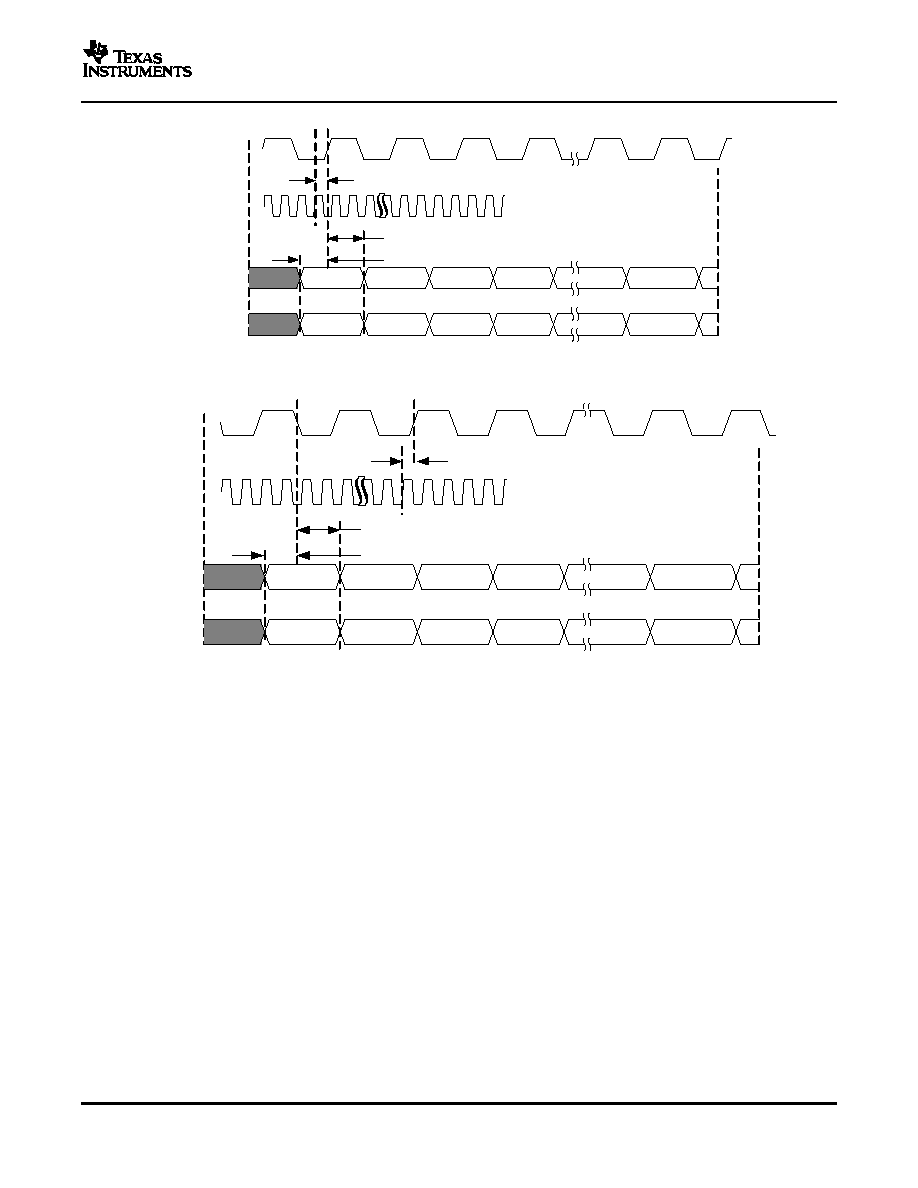
www.ti.com
PLLLOCK
CLK2
DA[15:0]
DB[15:0]
t
d(PLLLOCK)
t
h(DATA)
t
s(DATA)
A
0
A
1
A
2
A
3
A
N
A
N+1
B
0
B
1
B
2
B
3
B
N
B
N+1
PLLLOCK
CLK2
DA[15:0]
DB[15:0]
t
d(PLLLOCK)
t
h(DATA)
t
s(DATA)
A
0
A
1
A
2
A
3
A
N
A
N+1
B
0
B
1
B
2
B
3
B
N
B
N+1
DAC5687
SLWS164B FEBRUARY 2005 REVISED JUNE 2005
Figure 43. Dual Bus Mode Timing Diagram for External Clock Mode (PLLLOCK Rising Edge)
Figure 44. Dual Bus Mode Timing Diagram for External Clock Mode (PLLLOCK Falling Edge)
2. PLLVDD = 3.3 V (dual_clk can be 0 or 1 and is ignored): PLL CLOCK MODE
In PLL CLOCK MODE, you drive the DAC at the input sample rate (unless the data is mux'd) through
CLK1/CLK1C. CLK2/CLK2C is not used. In this case, there is no phase ambiguity on the clock. The DAC
generates the higher speed DAC sample rate clock using an internal PLL/VCO. In PLL clock mode, the user
provides a differential external reference clock on CLK1/CLK1C.
A type four phase-frequency detector (PFD) in the internal PLL compares this reference clock to a feedback
clock and drives the PLL to maintain synchronization between the two clocks. The feedback clock is generated
by dividing the VCO output by 1x, 2x, 4x, or 8x as selected by the prescaler (div[1:0]). The output of the
prescaler is the DAC sample rate clock and is divided down to generate clocks at ÷ 2, ÷4, and ÷ 8. The feedback
clock is selected by the registers sel(1:0), which is fed back to the PFD for synchronization to the input clock.
The feedback clock is also used for the data input rate, so the ratio of DAC output clock to feedback clock sets
the interpolation rate of the DAC5687. The PLLLOCK pin is an output indicating when the PLL has achieved
lock. An external RC low-pass PLL filter is provided by the user at pin LPF. See the Low-Pass Filter section for
filter setting calculations. This is the only mode where the LPF filter applies.
41

www.ti.com
CLK2
DA[15:0]
DB[15:0]
t
h(DATA)
t
s(DATA)
A
0
A
1
A
2
A
3
A
N
A
N+1
B
0
B
1
B
2
B
3
B
N
B
N+1
B0053-02
CLK
Buffer
CLK
Buffer
PFD
Charge
Pump
VCO
/1
/2
/4
/8
00
01
10
11
1
0
/2
Data
Latch
1 ´2
´1
0
00
01
10
11
/2
/2
0
1
CLK1
CLK1C
CLK2
LPF
DIV[1:0]
PLLVDD
PLLLOCK
PLLVDD
D[15:0]
INTERL
SEL[1:0]
Fdac
Fdac/2 2
´
Fdac/4 ´4
Fdac/4 ´4L
Fdac/8 ´8
Data
Lock
CLK2C
DAC5687
SLWS164B FEBRUARY 2005 REVISED JUNE 2005
Figure 45. Dual Bus Mode Timing Diagram (PLL Mode)
Figure 46. Clock Generation Architecture in PLL Mode
Power for the internal PLL blocks (PLLVDD and PLLGND) are separate from the other clock generation blocks
power (CLKVDD and CLKGND), thus minimizing PLL phase noise.
3) PLLVDD = 0 V and dual_clk = 1: DUAL CLOCK MODE
In DUAL CLOCK MODE, the DAC is driven at the DAC sample rate through CLK2/CLK2C and the input data
rate through CLK1/CLK1C. There are two options in dual clock mode: with FIFO (inv_plllock set) and without
FIFO (inv_plllock clear). If the FIFO is not used, the CLK1/CLK1C input is used to set the phase of the internal
clock divider. In this case, the edges of CLK1 and CLK2 must be aligned to within ±t
_align
(
Figure 47
), defined as
42

www.ti.com
f
align
+
1
2F
CLK2
*
0.5 ns
t
h
CLK2
CLK1
DA[15:0]
DB[15:0]
< t
align
t
s
t
h
CLK1
DA[15:0]
DB[15:0]
t
s
Input FIFO
DAC5687
SLWS164B FEBRUARY 2005 REVISED JUNE 2005
where f
CLK2
is the clock frequency at CLK2. For example, t
align
= 0.5 ns at f
CLK2
= 500 MHz and 1.5 ns at f
CLK2
=
250 MHz.
If the FIFO is enabled (inv_plllock set) in dual clock mode, then CLK1 is only used as an input latch (
Figure 48
)
and is independent from the internal divided clock generated from CLK2/CLK2C and there is no alignment
specification. However, the FIFO needs to be synchronized by one of the methods listed in SYNC_CNTL register
and the latency of the DAC can be up to one clock cycle different depending on the phase relationship between
CLK1 and the internally divided clock.
Figure 47. Dual Clock Mode Without FIFO
Figure 48. Dual Clock Mode With FIFO
The CDC7005 from Texas Instruments is recommended for providing phase aligned clocks at different
frequencies for this application.
In DAC clock mode, where the DAC5687 is clocked at the DAC update rate, the DAC5687 has an optional input
FIFO that allows latching of DA[15:0], DB[15:0] and PHSTR based on a user provided CLK1/CLK1C input or the
input data rate clock provided to the PLLLOCK pin. The FIFO can be bypassed by setting register fifo_bypass in
CONFIG0 to 1.
The input interface FIFO incorporates a four sample register file, an input pointer, and an output pointer.
Initialization of the FIFO pointers can be programmed to one of seven different sources.
43

www.ti.com
0
1
S
DA(15:0),
DB(15:0),
PHSTR
0
1
D Q
input
pointer
generation
PLLLOCK
MUX
CLK1
CLK1C
{PLLVDD,
inv_plllock, dual_clk}
MUX
clock
generator
resynchonized
da(15:0), db(15:0)
and phstr
sync source
{TXENABLE, PHSTR, QFLAG, DB(15),
DA(15) oneshot, SIF write, always off}
CLK2
CLK2C
PLL VCO
1
fifo_bypass
in_sel_d
in_sel_c
in_sel_b
in_sel_a
q_b
q_c
q_d
q_in
q_out
clk_in
clk_out
sel_q_a
sel_q_d
sel_q_c
sel_q_b
sync
D Q
DA(15:0),
DB(15:0),
PHSTR
0
1
S
D Q
S
0
1
S
D Q
,
output
pointer
generation
Q
D
DA(15) oneshot
0
Q
D
S
q_a
DAC5687
SLWS164B FEBRUARY 2005 REVISED JUNE 2005
Figure 49. DAC5687 Input FIFO Logic
Initialization of the FIFO block involves selecting and asserting a synchronization source. Initialization causes the
input and output pointers to be forced to an offset of 2; the input pointer will be forced to the in_sel_a state while
the output pointer will be forced to the sel_q_c state. This initialization of the input and output pointers can cause
discontinuities in a data stream and should therefore be handled at startup.
Table 11. Synchronization Source Selection
sync_fifo (2:0)
Synchronization Source
000
txenable pin
001
phstr pin
010
qflag pin
011
db(15)
100
da(15) first transition (one shot)
101
sync now with SIF write (always on)
110
sync source disabled (always off)
111
sync now with SIF write (always on)
44

www.ti.com
PHSTR
Q
D
QFLAG
TXENABLE
DB(15)
DA(15)
Q
D
sync_fifo = "100"
DA(15) first rising edge
PLLLOCK
MUX
CLK1
CLK1C
{PLLVDD, inv_plllock, dual_clk}
clk_in
MUX
D
clock
generator
PLL VCO
clk_out
sync
= "100"
sync_fifo(2:0)
1
000
001
010
011
100
101
110
111
Q
resync_fifo_in
CLK2
CLK2C
resync_fifo_out
1
0
Q
D
Q
D
Q
D
Q
D
D
Q
D
Q
D
Q
D
Q
D
Q
D
Q
D
Q
D
Q
Even/Odd Input Mode
Synchronization
DAC5687
SLWS164B FEBRUARY 2005 REVISED JUNE 2005
All possible sync sources are registered with clk_in and then passed through a synchronous rising edge detector.
Figure 50. DAC5687 FIFO Synchronization Source Logic
For example, if TXENABLE is selected as the sync source, a low-to-high transition on the TXENABLE pin causes
the pointers to be initialized.
Once initialized, the FIFO input pointer advances using clk_in and the output pointer advances using clk_out,
providing an elastic buffering effect. The phase relationship between clk_in and clk_out can wander or drift until
the output pointer overruns the input pointer or vice versa.
The DAC5687 has a double data rate input mode that allows both input ports to be used to multiplex data onto
one DAC channel (A). In the Even/Odd mode, the FIR3 filter can be used to interpolate the data by 2x. The
even/odd input mode is enabled by setting half_rate in CONFIG3. The maximum input rate for each port is 250
MSPS, for a combined rate of 500 MSPS.
The DAC5687 has several digital circuits that can be synchronized to a known state. The circuits that can be
synchronized are the fine mixer (NCO), coarse mixer (fixed fs/2 or fs/4 mixer), the FIFO input and output
pointers, and the internal clock divider.
45

www.ti.com
NCO Synchronization
PHSTR
PLLLOCK
MUX
CLK1
CLK1C
{PLLVDD, inv_plllock, dual_clk}
clk_in
clock
generator
CLK2
CLK2C
clk_out
FIFO
phstr sync to NCO
PLL VCO
clk_nco
phase
accumulator
reset
Q
D
,
}
Q
D
Q
D
Q
D
Q
D
Q
D
DAC5687
SLWS164B FEBRUARY 2005 REVISED JUNE 2005
Table 12. Synchronization in Different Clock Modes
Clock
PLLVDD
Serial Interface Register Bits
DA, DB,
Description
Mode
Pin
PHSTR, and
fifo_bypass
dual_clk
inv_plllock
TXENABLE
Latch
Single
0 V
1
0
0
PLLLOCK
Signal at the PLLLOCK output pin is used to clock the
External
rising edge
PHSTR signal into the chip. The PLLLOCK output
Clock
clock is generated by dividing the CLK2/CLK2C input
1
PLLLOCK
without
signal by the programmed interpolation and interface
falling edge
FIFO
settings.
Single
0 V
0
0
0
PLLLOCK
Signal at the PLLLOCK output pin is used to clock the
External
rising edge
PHSTR signal into the chip. The PLLLOCK output
Clock with
clock is generated by dividing the CLK2/CLK2C input
1
PLLLOCK
FIFO
signal by the programmed interpolation and interface
falling edge
settings. Enabling the FIFO allows the chip to function
with large loads on the PLLLOCK output pin at high
input rates. The FIFO must be initialized first in this
mode.
Dual
0 V
1
1
0
CLK1/CLK1C
The CLK1/CLK1C input signal is used to clock in the
External
PHSTR signal. CLK1/CLK1C and CLK2/CLK2C are
Clock
both input to the chip and the phase relationship must
without
be tightly controlled
FIFO
Dual
0 V
0
1
1
CLK1/CLK1C
The CLK1/CLK1C input signal is used to clock in the
External
PHSTR signal. CLK1/CLK1C and CLK2/CLK2C are
Clock with
both input to the chip, but no phase relationship is
FIFO
required. The FIFO input circuits are used to manage
the clock domain transfers. The FIFO must be
initialized in this mode.
PLL
3.3 V
1
0
0
CLK1/CLK1C
The CLK1/CLK1C input signal is used to clock in the
Enabled
PHSTR signal. The FIFO must be bypassed when the
PLL is enabled.
The phase accumulator in the NCO block (see the Fine Mixer (FMIX) section and
Figure 39
for a description of
the NCO) can be synchronously reset when PHSTR is asserted. The PHSTR signal passes through the input
FIFO block, using the input clock associated with the clocking mode. If the FIFO is enabled, there can be some
uncertainty in the exact instant the PHSTR synchronization signal arrives at the NCO accumulator due to the
elastic capabilities of the FIFO. For example, in dual-clock mode with the FIFO enabled, the internal clock
generator divides down the CLK2/CLK2C input signal to generate the FIFO output clock. The phase of this
generated clock will be unknown externally, resulting in an uncertainty of the exact PHSTR instant of as much as
a few input clock cycles.
Figure 51. Logic Path for PHSTR Synchronization Signal to NCO
46

www.ti.com
PHSTR
clk_in
clk_out
phstr at FIFO
output
clk_nco
phase
accumulator
reset
phase_accum
only needs to be asserted for one clk_in period
Input delay line + FIFO delay
13 clk_nco cycles
Coarse Mixer (CMIX) Synchronization
DAC5687
SLWS164B FEBRUARY 2005 REVISED JUNE 2005
The serial interface includes a sync_nco bit in register SYNC_CNTL, which needs to be set for the PHSTR input
signal to initialize the phase accumulator.
The NCO uses a rising edge detector to perform the synchronous reset of the phase accumulator. Due to the
pipelined nature of the NCO, the latency from the phstr sync signal at the FIFO output to the instant the phase
accumulator is cleared is 13 f
NCO
clock cycles (f
NCO
= f
DAC
in X4 mode, f
NCO
= f
DAC
/2 in X2, X4L, and X8 modes).
In 2x interpolation mode with the inverse sinc filter disabled, overall latency from PHSTR input to DAC output is
~100 input clock cycles.
Figure 52. NCO Phase Accumulator Reset Synchronization Timing
The coarse mixer implements the f
DAC
/2 and f
DAC
/4 (and f
DAC
/4) fixed complex mixing operation using simple
complements of the datapath signals to create the proper sequences. The sequences are controlled using a
simple counter and this counter can be synchronously reset using the PHSTR signal.
Similar to the NCO, the PHSTR signal used by the coarse mixer is from the FIFO output. This introduces the
same uncertainty effect due to the FIFO input to output pointer relationship. Bypassing the FIFO and using the
dual external clock mode without FIFO eliminates this uncertainty for systems using multiple DAC5687 devices
when this cannot be tolerated. Using the internal PLL, as with the NCO, allows the complete control and
synchronization of the coarse mixer.
47

www.ti.com
PHSTR
PLLLOCK
MUX
CLK1
CLK1C
{PLLVDD, inv_plllock, dual_clk}
clk_in
Clock
Genera-
tor
CLK2
CLK2C
clk_out
FIFO
phstr sync to coarse mixer
PLL VCO
clk_cmix
Sequencer
Reset
sync_cm
D Q
D Q
D Q
D Q
D Q
D Q
Sequencer
Reset
PHSTR
clk_in
Only needs to be high for one clk_in period
clk_cmix
phstr at FIFO
Output
Sequencer
fs/2
clk_out
Input delay line + FIFO delay
Sequencer
fs/4
0
90
180
180 270
0
180
0
0
90
DAC5687
SLWS164B FEBRUARY 2005 REVISED JUNE 2005
Figure 53. Logic Path for PHSTR Synchronization Signal to CMIX Reset
To enable the PHSTR synchronous reset, the serial interface bit sync_cm in register SYNC_CNTL must be set.
The coarse mixer sequence counter will be held reset when PHSTR is low and operates when PHSTR is high.
Figure 54. CMIX Reset Synchronization Timing
In addition to the reset function provided by the PHSTR signal, the phstr_del(1:0) bits in register ATEST allow
the user to select the initial (reset) state. Changing the cm_mode lower 2 bits produces the same phase shift
results.
Table 13. Initial State of CMIX After Reset
Fix Mix Selection
phstr_del(1:0)
Initial State at PHSTR
f
S
/2
00 and 10
Normal
f
S
/2
01 and 11
180 degree shift
f
S
/4
00
Normal
f
S
/4
01
90 degree shift
48

www.ti.com
Input Clock Synchronization of Multiple DAC5687s
CDC7005
# 1
Y0
Y0
Y0
Y0
Y1
Y1
Y1
Y1
Y2
Y2
Y2
Y2
Y3
Y3
Y3
Y3
CDC7005
# 2
Y0
Y0
Y0
Y0
Y1
Y1
Y1
Y1
Y2
Y2
Y2
Y2
Y3
Y3
Y3
Y3
DAC5687
# 1
CLK1
CLK1C
CLK2
CLK2C
DAC5687
# 2
CLK1
CLK1C
CLK2
CLK2C
DAC5687
# 3
CLK1
CLK1C
CLK2
CLK2C
DAC5687
# 4
CLK1
CLK1C
CLK2
CLK2C
Ref
Ref
f
INPUT
f
INPUT
f
DAC
f
INPUT
f
DAC
f
INPUT
f
DAC
f
INPUT
f
DAC
f
INPUT
f
DAC
f
INPUT
f
DAC
f
INPUT
f
DAC
f
INPUT
f
DAC
Reference Operation
DAC5687
SLWS164B FEBRUARY 2005 REVISED JUNE 2005
Table 13. Initial State of CMIX After Reset (continued)
Fix Mix Selection
phstr_del(1:0)
Initial State at PHSTR
f
S
4
10
180 degree shift
f
S
/4
11
270 degree shift
For applications where multiple DAC5687 chips are used, clock synchronization is best achieved by using
dual-clock mode with the FIFO disabled or the PLL-clock mode. In the dual-clock mode with FIFO disabled, an
appropriate clock PLL such as the CDC7005 is required to provide the DAC and input rate clocks that meet the
skew requirement t_align (see
Figure 47
). An example for synchronizing multiple DAC5687 devices in dual clock
mode with two CDC7005 is shown in
Figure 55
. When using the internal PLL-clock mode, synchronization of
multiple using PHSTR is completely deterministic due to the phase/frequency detector in the PLL feedback loop.
All chips using the same CLK1/CLK1C input clock will have identical internal clocking phases.
Figure 55. Block Diagram for Clock Synchronization of Multiple DAC5687 Devices in Dual-Clock Mode
The DAC5687 comprises a bandgap reference and control amplifier for biasing the full-scale output current. The
full-scale output current is set by applying an external resistor RBIAS to pin BIASJ. The bias current IBIAS
through resistor RBIAS is defined by the on-chip bandgap reference voltage and control amplifier. The full-scale
output current equals 16 times this bias current. The full-scale output current IOUTFS can thus be expressed as:
IOUT
FS
= 16 × I
BIAS
= 16 × V
EXTIO
/ R
BIAS
where V
EXTIO
is the voltage at terminal EXTIO. The bandgap reference voltage delivers an accurate voltage of
1.2 V. This reference is active when terminal EXTLO is connected to AGND. An external decoupling capacitor
C
EXT
of 0.1 µF should be connected externally to terminal EXTIO for compensation. The bandgap reference can
additionally be used for external reference operation. In that case, an external buffer with high impedance input
should be applied in order to limit the bandgap load current to a maximum of 100 nA. The internal reference can
be disabled and overridden by an external reference by connecting EXTLO to AVDD. Capacitor C
EXT
may hence
be omitted. Terminal EXTIO thus serves as either input or output node.
49

www.ti.com
DAC Transfer Function
Analog Current Outputs
DAC5687
SLWS164B FEBRUARY 2005 REVISED JUNE 2005
The full-scale output current can be adjusted from 20 mA down to 2 mA by varying resistor R
BIAS
or changing the
externally applied reference voltage. The internal control amplifier has a wide input range, supporting the
full-scale output current range of 20 mA.
The CMOS DAC's consist of a segmented array of NMOS current sinks, capable of sinking a full-scale output
current up to 20 mA. Differential current switches direct the current of each current source through either one of
the complementary output nodes IOUT1 or IOUT2. Complementary output currents enable differential operation,
thus canceling out common mode noise sources (digital feed-through, on-chip and PCB noise), dc offsets, even
order distortion components, and increasing signal output power by a factor of two.
The full-scale output current is set using external resistor R
BIAS
in combination with an on-chip bandgap voltage
reference source (+1.2 V) and control amplifier. Current I
BIAS
through resistor R
BIAS
is mirrored internally to
provide a full-scale output current equal to 16 times IBIAS. The full-scale current IOUT
FS
can be adjusted from 20
mA down to 2 mA.
The relation between IOUT1 and IOUT2 can be expressed as:
IOUT1 = -IOUT
FS
IOUT2
We will denote current flowing into a node as - current and current flowing out of a node as + current. Since the
output stage is a current sink the current can only flow from AVDD into the IOUT1 and IOUT2 pins. If IOUT2 = -
5 mA and IO(FS) = 20 mA then:
IOUT1 = -20 (-5) = -15 mA
The output current flow in each pin driving a resistive load can be expressed as:
IOUT1 = IOUT
FS
× CODE / 65536
IOUT2 = IOUT
FS
× (65535 CODE) / 65536
where CODE is the decimal representation of the DAC data input word.
For the case where IOUT1 and IOUT2 drive resistor loads R
L
directly, this translates into single ended voltages
at IOUT1 and IOUT2:
VOUT1 = AVDD I IOUT1 I × R
L
VOUT2 = AVDD I IOUT2 I × R
L
Assuming that the data is full scale (65535 in offset binary notation) and the R
L
is 25
, the differential voltage
between pins IOUT1 and IOUT2 can be expressed as:
VOUT1 = AVDD I -20 mA I x 25
= 2.8 V
VOUT2 = AVDD I -0 mA I x 25
= 3.3 V
VDIFF = VOUT1 VOUT2 = 0.5 V
Note that care should be taken not to exceed the compliance voltages at node IOUT1 and IOUT2, which would
lead to increased signal distortion.
Figure 56
shows a simplified schematic of the current source array output with corresponding switches.
Differential switches direct the current of each individual NMOS current source to either the positive output node
IOUT1 or its complementary negative output node IOUT2. The output impedance is determined by the stack of
the current sources and differential switches, and is typically >300 k
in parallel with an output capacitance of 5
pF.
The external output resistors are referred to an external ground. The minimum output compliance at nodes
IOUT1 and IOUT2 is limited to AVDD 0.5 V, determined by the CMOS process. Beyond this value, transistor
breakdown may occur resulting in reduced reliability of the DAC5687 device. The maximum output compliance
voltage at nodes IOUT1 and IOUT2 equals AVDD + 0.5 V. Exceeding the minimum output compliance voltage
adversely affects distortion performance and integral non-linearity. The optimum distortion performance for a
single-ended or differential output is achieved when the maximum full-scale signal at IOUT1 and IOUT2 does not
exceed 0.5 V.
50

www.ti.com
IOUT1
IOUT2
S(1)
S(1)C
R
LOAD
R
LOAD
S(2)
S(2)C
S(N)
S(N)C
AVDD
S0032-01
IOUT1
1:1
IOUT2
50
50
R
LOAD
50
100
AVDD (3.3 V)
AVDD (3.3 V)
S0033-01
DAC5687
SLWS164B FEBRUARY 2005 REVISED JUNE 2005
Figure 56. Equivalent Analog Current Output
The DAC5687 can be easily configured to drive a doubly terminated 50-
cable using a properly selected RF
transformer.
Figure 57
and
Figure 58
show the 50-
doubly terminated transformer configuration with 1:1 and
4:1 impedance ratio, respectively. Note that the center tap of the primary input of the transformer has to be
connected to AVDD to enable a dc-current flow. Applying a 20-mA full-scale output current would lead to a 0.5
V
PP
for a 1:1 transformer and a 1-V
PP
output for a 4:1 transformer. The low dc-impedance between the IOUT1 or
IOUT2 and the transformer center tap sets the center of the ac-signal at AVDD, so the 1-V
PP
output for the 4:1
transformer results in an output between AVDD + 0.5 V and AVDD 0.5 V.
Figure 57. Driving a Doubly Terminated 50-
Cable Using a 1:1 Impedance Ratio Transformer
51

www.ti.com
IOUT1
4:1
IOUT2
100
100
R
LOAD
50
AVDD (3.3 V)
AVDD (3.3 V)
S0033-02
Combined Output Termination
S0069-01
IOUTA1
1:1
R
LOAD
50
IOUTA2
AVDD (3.3 V)
IOUTB1
IOUTB2
DAC5687
SLWS164B FEBRUARY 2005 REVISED JUNE 2005
Figure 58. Driving a Doubly Terminated 50-
Cable Using a 4:1 Impedance Ratio Transformer
The DAC5687 DAC A and DAC B outputs can be summed together as shown in
Figure 59
to provide a 40-mA
full-scale output for increased output power.
Figure 59. Combined Output Termination Using a 1:1 Impedance Ratio Transformer into 50-
Load
For the case where the digital codes for the two DACs are identical, the termination results in a full scale swing
of 2 V
PP
into the 50-
load, or 10 dBm. This is 6 dB higher than the 4:1 output termination recommended for a
single DAC output.
There are two methods to produce identical DAC codes. In modes where there is mixing between digital
channels A and B, i.e., when channels A and B are isolated, the identical data can be sent to both input ports to
produce identical DAC codes. Channels A and B are isolated when FMIX is disabled, the QMC is disabled or
enabled with QMC phase register set to 0, and CMIX is disabled or set to f
DAC
/2. Note that frequency
upconversion is still possible using the high-pass filter setting and CMIX f
DAC
/2.
Alternatively, by applying the input data on one input port only and setting the other input port to mid-scale (zero),
the NCO can be used to duplicate the output of the active input channel in the other channel by setting the
frequency to zero, phase to 8192 and NCO_GAIN = 1 and QMC gain = 1446. Assuming I(t) is the wanted signal
and Q(t) = 0, this is demonstrated by the simplification of the NCO equations in the Fine Mixer (FMIX) section:
I
OUT
(t) = (I
IN
(t)cos(2
x 0 x t +
/4) 0 x sin((2
x 0 x t +
/4)) x 2
(1 1)
= I
IN
(t)cos(
/4) = I
IN
(t)/2
½
Q
OUT
(t) = (I
IN
(t)sin(2
x 0 x t +
/4) + 0 x cos(2
x 0 x t +
/4)) x 2
(1 1)
= I
IN
(t)sin(
/4) = I
IN
(t)/2
½
52

www.ti.com
Digital Inputs
DA[15:0]
DB[15:0]
SLEEP
PHSTR
TxENABLE
QFLAG
SDIO
SCLK
SDENB
Internal
Digital In
IOVDD
IOGND
RESETB
Internal
Digital In
IOVDD
IOGND
Clock Inputs
CLK
Internal
Digital In
CLKC
CLKGND
R1
10 k
CLKVDD
R1
10 k
R2
10 k
R2
10 k
CLKVDD
CLKVDD
S0028-01
DAC5687
SLWS164B FEBRUARY 2005 REVISED JUNE 2005
Applying the QMC gain of 1446, equivalent to 2
½
, increases the signal back to unity gain through the FMIX and
the QMC blocks.
Note that with this termination, the DAC side of the transformer is not 50-
terminated and therefore may result
in reflections when used with a cable output.
Figure 60
shows a schematic of the equivalent CMOS digital inputs of the DAC5687. DA[0..15], DB[0..15],
SLEEP, PHSTR, TXENABLE, QFLAG, SDIO, SCLK, and SDENB have pull-down resistors and RESETB has a
pull-up resistor internal to the DAC5687. See the specification table for logic thresholds.
Figure 60. CMOS/TTL Digital Equivalent Input
Figure 61
shows an equivalent circuit for the clock input.
Figure 61. Clock Input Equivalent Circuit
Figure 62
,
Figure 63
, and
Figure 64
show various input configurations for driving the differential clock input
(CLK/CLKC).
53

www.ti.com
R
T
200
CLK
1:4
CLKC
Termination Resistor
Swing Limitation
Optional, May Be Bypassed
for Sine Wave Input
C
AC
0.1
µ
F
S0029-01
R
opt
22
CLK
1:1
CLKC
Optional, Reduces
Clock Feedthrough
C
AC
0.01
µ
F
TTL/CMOS
Source
R
opt
22
CLK
CLKC
Node CLKC Internally Biased
to CLKVDD 2
TTL/CMOS
Source
0.01
µ
F
S0030-01
R
T
130
C
AC
0.1
µ
F
C
AC
0.1
µ
F
R
T
130
V
TT
Differential
ECL
or
(LV)PECL
Source
+
CLK
CLKC
R
T
82.5
R
T
82.5
100
S0031-01
Power Up Sequence
DAC5687
SLWS164B FEBRUARY 2005 REVISED JUNE 2005
Figure 62. Preferred Clock Input Configuration
Figure 63. Driving the DAC5687 With a Single-Ended TTL/CMOS Clock Source
Figure 64. Driving the DAC5687 With Differential ECL/PECL Clock Source
In all conditions, bring up DVDD first. If PLLVDD is powered (PLL on), CLKVDD should be powered before or
simultaneously with PLLVDD. AVDD, CLKVDD, and IOVDD can be powered simultaneously or in any order.
Within AVDD, the multiple AVDD pins should be powered simultaneously.
54

www.ti.com
Sleep Mode
Application Information
Designing the PLL Loop Filter
DAC5687
SLWS164B FEBRUARY 2005 REVISED JUNE 2005
There are no specific requirements on the ramp rate for the supplies.
The DAC5687 features a power-down mode that turns off the output current and reduces the supply current to
less than 5 mA over the supply range of 3 V to 3.6 V and temperature range. The power-down mode is activated
by applying a logic level 1 to the SLEEP pin (e.g., by connecting pin SLEEP to AVDD). An internal pull-down
circuit at node SLEEP ensures that the DAC5687 is enabled if the input is left disconnected. Power-up and
power-down activation times depend on the value of external capacitor at node EXTIO. For a nominal capacitor
value of 0.1-µF, power down takes less than 5 µs and approximately 3 ms to power back up.
Table 14. Optimum DAC5687 PLL Settings
f
DAC
(MHZ)
pll_freq
pll_kv
pll_div (1:0)
f
VCO
/ f
DAC
Estimated G
VCO
(MHz/V)
25 to
0
1
11
8
380
28.125
28.125 to
0
0
11
8
250
46.25
46.25 to 60
0
1
11
8
300
60 to
1
0
11
8
130
61.875
61.875 to
1
1
11
8
225
65
65 to 92.5
0
0
10
4
250
92.5 to 120
0
1
10
4
300
120 to
1
0
10
4
130
123.75
123.75 to
1
1
10
4
225
130
130 to 185
0
0
01
2
250
185 to 240
0
1
01
2
300
240 to
1
0
01
2
130
247.5
247.5 to
1
1
01
2
225
260
260 to 370
0
0
00
1
250
370 to 480
0
1
00
1
300
480 to 495
1
0
00
1
130
495 to 520
1
1
00
1
225
The optimized DAC5687 PLL settings based on the VCO frequency MIN and MAX values (see the digital
specifications) as a function of f
DAC
are listed in
Table 14
. To minimize phase noise at a given f
DAC
, pll_freq,
pll_kv, and the pll_div have been chosen so G
VCO
is minimized and within the MIN and MAX frequency for a
given setting.
For example, if f
DAC
= 245.76 MHz, pll_freq is set to 1, pll_kv is set to 0 and pll_div(1:0) is set to 01 (divide by 2)
to lock the VCO at 491.52 MHz.
The external loop filter components C1, C2, and R1 are set by the G
VCO
, N = f
VCO
/f
DATA
= f
VCO
x
Interpolation/f
DAC
, the loop phase margin
d
and the loop bandwidth
d
. Except for applications where abrupt
clock frequency changes require a fast PLL lock time, it is suggested that
d
be set to at least 80 degrees for
stable locking and suppression of the phase noise side lobes. Phase margins of 60 degrees or less can be
sensitive to board layout and decoupling details.
C1, C2, and R1 are then calculated by the following equations
55

www.ti.com
C1
+ t
1 1
*
t
2
t
3
C2
+
t
1
* t
2
t
3
R1
+
t
3
2
t
1 (
t
3
* t
2)
(1)
t
1
+
K
d
Kvco
w
2
d
tan
f
d
)
sec
f
d
t
2
+
1
w
d
tan
f
d
)
sec
f
d
t
3
+
tan
f
d
)
sec
f
d
w
d
(2)
DAC5687 Passive Interface-to-Analog Quadrature Modulators
DAC5687
SLWS164B FEBRUARY 2005 REVISED JUNE 2005
where,
and
charge pump current: iqp = 1 mA
vco gain: K
VCO
= 2
xG
VCO
rad/V
FVCO/FDATA: N = {2, 4, 8, 16, 32}
phase detector gain: K
d
= iqp
×
(2
×
N) 1 A/rad
An Excel spreadsheet is provided by Texas Instruments for automatically calculating the values for C1, C2, and
R.
Completing the example given above with:
Parameter
Value
Units
G
VCO
1.30E+02
MHz/V
d
0.50E+00
MHz
N
4
d
80
Degrees
The component values are:
C1 (F)
C2 (F)
R (
)
3.74E-08
2.88E-10
9.74E+01
As the PLL characteristics are not sensitive to these components, the closest 20% tolerance capacitor and 1%
tolerance resistor values can be used. If the calculation results in a negative value for C2 or an unrealistically
large value for C1, then the phase margin may need to be reduced slightly.
The DAC5687 has a maximum 20-mA full-scale output and a compliance range of AVDD
±
0.5 V. The TRF3701
or TRF3702 analog quadrature modulators (AQM) require a common-mode of approximately 3.7 V and 1.5 V to
2-V
PP
differential swing. A resistive network as shown in
Figure 65
can be used to translate the common mode
voltage between the DAC5687 and TRF3701 or TRF3702. The voltage at the DAC output pins for a full-scale
sine wave is centered at approximately AVDD with a 1-V
PP
single ended (2-V
PP
differential). The voltage at the
TRF3701/2 input pins is centered at 3.7 V and swings 0.76-V
PP
single ended (1.56-V
PP
differential), or 2.4 dB of
insertion loss.
56

www.ti.com
B0046-01
TRF3701
TRF3702
GND
205
205
15.4
15.4
15.4
15.4
GND
205
205
5 V
50
50
5 V
50
50
B0046-02
AQM
69.8
69.8
124
124
124
124
69.8
69.8
-5 V
453
453
-5 V
453
453
5 V
5 V
Non-Harmonic Clock-Related Spurious Signals
DAC5687
SLWS164B FEBRUARY 2005 REVISED JUNE 2005
Figure 65. DAC5687 Passive Interface to TRF3701/2 Analog Quadrature Modulator
Changing the voltage levels and resistor values enable other common-mode voltages at the analog quadrature
modulator input. For example, the network shown in
Figure 66
can produce a 1.5-V common mode at the analog
quadrature modulator input, with a 0.78-V
PP
single-ended swing (1.56-V
PP
differential swing), or 0.2-dB insertion
loss.
Figure 66. DAC5687 Passive Interface With 1.5-V Common Mode at AQM Input
In interpolating DACs, imperfect isolation between the digital and DAC clock circuits generate spurious signals at
frequencies related to the DAC clock rate. The digital interpolation filters in these DACs run at sub-harmonic
frequencies of the output rate clock, where these frequencies are f
DAC
/2
N
, N = 1 - 3. For example, for X2 mode
there is only one interpolation filter running at f
DAC
/2; for X4 and X4L modes, on the other hand, there are two
interpolation filters running at f
DAC
/2 and f
DAC
/4. In X8 mode, there are three interpolation filters running at f
DAC
/2,
f
DAC
/4, and f
DAC
/8. These lower-speed clocks for the interpolation filter mix with the DAC clock circuit and create
spurious images of the wanted signal and second Nyquist-zone image at offsets of f
DAC
/2
N
.
57

www.ti.com
Location of the Spurious Signals
f
SIG
/f
DAC
-0.5
-0.4
-0.3
-0.2
-0.1
-0.0
0.1
0.2
0.3
0.4
0.5
0.0
0.1
0.2
0.3
0.4
0.5
Spurious Frequency/f
D
A
C
G026
f
SIG
f
SIG
- f
DAC
/2
(a) Complex Output in X2 Mode
(b) Real Output in X2 Mode
f
SIG
/f
DAC
0.00
0.05
0.10
0.15
0.20
0.25
0.30
0.35
0.40
0.45
0.50
0.0
0.1
0.2
0.3
0.4
0.5
Spurious Frequency/f
D
A
C
G027
f
SIG
f
SIG
- f
DAC
/2
DAC5687
SLWS164B FEBRUARY 2005 REVISED JUNE 2005
To calculate the non-harmonic clock related spurious signals for a particular condition, we first determine the
location of the spurious signals and then the amplitude.
The location of the spurious signals is determined by the DAC5687 output frequency (f
SIG
) and whether the
output is used as a dual output complex signal to be fed to an analog quadrature modulator (AQM) or as a real
IF signal from a single DAC output.
Figure 67
shows the location of spurious signals for X2 mode as a function of f
SIG
/f
DAC
. For complex outputs, the
spurious frequencies cover a range of -0.5 x f
DAC
to 0.5 x f
DAC
, with the negative complex frequency indicating
that the spurious signal will fall in the opposite sideband at the output of the QAM from the wanted signal. For the
real output, the phase information for the spurious signal is lost, and therefore what was a negative frequency for
the complex output is a positive frequency for a real output.
For the X2 mode, there is one spurious frequency with an absolute frequency less than 0.5 x f
DAC
. For a complex
output in X2 mode, the spurious signal will always be offset f
DAC
/2 from the wanted signal at f
SIG
- f
DAC
/2. For a
real output, as f
SIG
approaches f
DAC
/4, the spurious signal frequency falls at f
DAC
/2-f
SIG
, which will also approach
f
DAC
/4.
Figure 67. Frequency of Clock Mixing Spurious Images in X2 Mode
Figure 68
shows the location of spurious signals for X4 and X4L mode as a function of f
SIG
/f
DAC
. The addition of
the f
DAC
/4 clock frequency for the first interpolation filter creates three new spurious signals. For a complex
output, the nearest spurious signals are f
DAC
/4 offset from f
SIG
. For a real output, the signal due to f
SIG
- f
DAC
/4
and f
SIG
- f
DAC
x 3/4 falls in band as f
SIG
approaches f
DAC
/8 and f
DAC
x 3/8. This creates optimum real output
frequencies f
SIG
= f
DAC
x N/16 (N = 1, 3, 5, and 7), where the minimum spurious product offset from f
SIG
is f
DAC
/8.
58

www.ti.com
(a) Complex Output in X4 and X4L Modes
(b) Real Output in X4 and X4L Modes
f
SIG
/f
DAC
-0.5
-0.4
-0.3
-0.2
-0.1
0.0
0.1
0.2
0.3
0.4
0.5
0.0
0.1
0.2
0.3
0.4
0.5
Spurious Frequency/f
D
A
C
G028
f
SIG
- f
DAC
*3/4
f
SIG
- f
DAC
/2
f
SIG
- f
DAC
/4
f
SIG
+ f
DAC
/4
f
SIG
f
SIG
/f
DAC
0.00
0.05
0.10
0.15
0.20
0.25
0.30
0.35
0.40
0.45
0.50
0.0
0.1
0.2
0.3
0.4
0.5
Spurious Frequency/f
D
A
C
G029
f
SIG
+ f
DAC
/4
f
SIG
- f
DAC
*3/4
f
SIG
- f
DAC
/4
f
SIG
f
SIG
- f
DAC
/2
(a) Complex Output in X8 Mode
(b) Real Output in X8 Mode
f
SIG
/f
DAC
-0.5
-0.4
-0.3
-0.2
-0.1
-0.0
0.1
0.2
0.3
0.4
0.5
0.0
0.1
0.2
0.3
0.4
0.5
Spurious Frequency/f
D
A
C
G030
f
SIG
+ f
DAC
/4
f
SIG
- f
DAC
*3/4
f
SIG
- f
DAC
/4
f
SIG
- f
DAC
/2
f
SIG
- f
DAC
*7/8
f
SIG
f
SIG
- f
DAC
/8
f
SIG
+ f
DAC
/8
f
SIG
/f
DAC
0.00
0.05
0.10
0.15
0.20
0.25
0.30
0.35
0.40
0.45
0.50
0.0
0.1
0.2
0.3
0.4
0.5
Spurious Frequency/f
D
A
C
G031
f
SIG
- f
DAC
/4
f
SIG
- f
DAC
*7/8
f
SIG
- f
DAC
/2
f
SIG
+ f
DAC
/4
f
SIG
+ f
DAC
/8
f
SIG
f
SIG
- f
DAC
/8
f
SIG
- f
DAC
*3/4
Amplitude of the Spurious Signals
DAC5687
SLWS164B FEBRUARY 2005 REVISED JUNE 2005
Figure 68. Frequency of Clock Mixing Spurious Images in X4 and X4L Modes
Figure 69
shows the location of spurious signals for X8 mode as a function of f
SIG
/f
DAC
. The addition of the f
DAC
/8
clock frequency for the first interpolation filter creates four new spurious signals. For a complex output, the
nearest spurious signals are f
DAC
/8 offset from f
SIG
. For a real output, the optimum real output frequencies f
SIG
=
f
DAC
x N/16 (N = 3 and 5), where the minimum spurious product offset from f
SIG
is f
DAC
/8.
Figure 69. Frequency of Clock Mixing Spurious Images in X4 and X4L Modes
The spurious signal amplitude is sensitive to factors such as temperature, voltage, and process. Typical worst
case estimates to account for the variation over these factors are provided below as design guidelines.
59

www.ti.com
(a) X2 Mode
(b) X4L Mode
f
DAC
- MHz
0
10
20
30
40
50
60
70
80
90
0
100
200
300
400
500
Spurious Amplitude - dBc
G032
f
DAC
/2
f
DAC
- MHz
0
10
20
30
40
50
60
70
80
90
100
0
100
200
300
400
500
Spurious Amplitude - dBc
G033
f
DAC
/2
f
DAC
/4
(c) X4 Mode
(d) X8 Mode
f
DAC
- MHz
0
10
20
30
40
50
60
70
80
90
100
0
100
200
300
400
500
Spurious Amplitude - dBc
G034
f
DAC
/2
f
DAC
/4
f
DAC
x 3/4
f
DAC
- MHz
0
10
20
30
40
50
60
70
80
90
100
0
100
200
300
400
500
Spurious Amplitude - dBc
G035
f
DAC
/2
f
DAC/
4
f
DAC
x 3/4
f
DAC
/8
f
DAC
x 7/8
DAC5687
SLWS164B FEBRUARY 2005 REVISED JUNE 2005
Figure 70
and
Figure 71
show the typical worst case spurious signal amplitudes vs f
DAC
for a signal frequency
f
SIG
= 11 x f
DAC
/32 in each mode for PLL on (PLL clock mode) and PLL off (external and dual clock modes). Each
spurious signal (f
DAC
/2, f
DAC
/4 and f
DAC
/8) has its own curve. The spurious signal amplitudes can then be
adjusted for the exact signal frequency f
SIG
by applying the amplitude adjustment factor shown in
Figure 72
. The
amplitude adjustment factor is the same for each spurious signal (f
DAC
/2, f
DAC
/4, and f
DAC
/8) and is normalize for
f
SIG
= 11 x f
DAC
/32.
Figure 70. Clock Related Spurious Signal Amplitude With PLL Off for f
SIG
= 11 x f
DAC
/ 32
60

www.ti.com
(a) X2 Mode
(b) X4L Mode
(c) X4 Mode
(d) X8 Mode
f
DAC
- MHz
0
10
20
30
40
50
60
0
100
200
300
400
500
Spurious Amplitude - dBc
G036
f
DAC
/2
f
DAC
- MHz
0
10
20
30
40
50
60
0
100
200
300
400
500
Spurious Amplitude - dBc
G037
f
DAC
/2
f
DAC
/4
f
DAC
x 3/4
f
DAC
- MHz
0
10
20
30
40
50
60
70
0
100
200
300
400
500
Spurious Amplitude - dBc
G038
f
DAC
/2
f
DAC
/4
f
DAC
- MHz
0
10
20
30
40
50
60
70
0
100
200
300
400
500
Spurious Amplitude - dBc
G039
f
DAC
/2
f
DAC
/8
f
DAC
x 7/8
f
DAC
/4
f
DAC
x 3/4
DAC5687
SLWS164B FEBRUARY 2005 REVISED JUNE 2005
Figure 71. Clock Related Spurious Signal Amplitude With PLL On for f
SIG
= 11 x f
DAC
/ 32
61

www.ti.com
f
SIG
/f
DAC
-20
-10
0
10
20
30
40
0.0
0.1
0.2
0.3
0.4
0.5
0.6
0.7
0.8
0.9
1.0
Amplitude Adjustment - dB
G040
DAC5687
SLWS164B FEBRUARY 2005 REVISED JUNE 2005
Figure 72. Amplitude Adjustment Factor for f
SIG
The steps for calculating the non-harmonic spurious signals are:
1. Find the spurious signal frequencies for the appropriate mode from
Figure 67
,
Figure 68
, or
Figure 69
.
2. Find the amplitude for each spurious frequency for the appropriate mode from
Figure 70
or
Figure 71
.
3. Adjust the amplitude of the spurious signals for f
SIG
using the adjustment factor in
Figure 72
.
Consider Example 1 with the following conditions:
1. X4 Mode
2. Pll off
3. Complex Output
4. f
DAC
= 500 MHz
5. f
SIG
= 160 MHz = 0.32 x f
DAC
First, the location of the spurious signals is found for the x4 complex output in
Figure 68
(a). Three spurious
signals are present in the range -0.5 x f
DAC
to 0.5 x f
DAC
: two from f
DAC
/4 (35 MHz and -215 MHz) and one from
f
DAC
/2 (-90 MHz). Consulting
Figure 70
©), the raw amplitudes for f
DAC
/2 and f
DAC
/4 are 60 and 58 dBc,
respectively. From
Figure 72
, the amplitude adjustment factor for f
SIG
= 0.32 x f
DAC
is estimated at ~ 1 dB and so
the f
DAC
/2 and f
DAC
/4 are adjusted to 61 and 59 dBc.
Table 15. Example # 1 for Calculating Spurious Signals
Spurious Sig-
Frequency/f
DAC
Frequency
Raw Amplitude (dBc)
Adjusted Amplitude (dBc)
nal
(MHz)
f
DAC
/4
0.7
35
58
59
f
DAC
/2
-0.18
-90
60
61
f
DAC
/4
-0.43
-215
58
59
Now consider Example 2 with the following conditions:
1. X2 Mode
2. PLL on
3. Real output
4. f
DAC
= 400 MHz
5. f
SIG
= 70 MHz = 0.175 x f
DAC
62

www.ti.com
Schematic and Layout Recommendations
Application Examples
Application Example: Real IF Radio
DAC5687
SLWS164B FEBRUARY 2005 REVISED JUNE 2005
First, the location of the spurious signals is found for the X2 real output in
Figure 67
(b). One spurious signals is
present in the range 0 to 0.5
×
f
DAC
at 0.325
×
f
DAC
(see
Table 16
). Consulting
Figure 71
(a), the raw amplitude for
f
DAC
/2 is 47 dBc. From
Figure 72
, the amplitude adjustment factor for f
SIG
= 0.175 x f
DAC
is estimated at ~ 6 dB,
and so the f
DAC
/2 and f
DAC
/4 is adjusted to 53 dBc.
Table 16. Example # 2 for Calculating Spurious Signals
Spurious Sig-
Frequency/f
DAC
Frequency
Raw Amplitude (dBc)
Adjusted Amplitude (dBc)
nal
(MHz)
f
DAC
/2
0.325
130
47
53
The DAC5687 clock is sensitive to fast transitions of input data on pins DA0, DA1, and DA2 (55, 54, and 53) due
to coupling to DVDD pin 56. The noise-like spectral energy of the DA[0-2] couples into the DAC clock resulting in
increased jitter. This significantly improves by using a 10-
resistor between DVDD and pin 56 in addition to
10-pF capacitor to DGND, as implemented on the DAC5687EVM (see the DAC5687 EVM user's guide -
SLWU017)
. Pin 56 draws only approximately 2 mA of current and the 0.02-V voltage drop across the resistor is
acceptable for DVDD voltages within the MINIMUM and MAXIMUM specifications. It is also recommended that
the transition rate of the input lines be slowed by inserting series resistors near the data source. The optimized
value of the series resistor depends on the capacitance of the trace between the series resistor and DAC5687
input pin. For a 2-3 inch trace, a 22-
to 47-
resistor would be recommended.
The effect of DAC clock jitter on the DAC output signal is worse for signals at higher signal frequencies. For low
IF (< 75 MHz) or baseband signals, there is little degradation of the output signal. However, for high IF (> 75
MHz) the DAC clock jitter may result in an elevated noise floor, which often appears as broad humps in the DAC
output spectrum. It is recommended for signals above 75 MHz that the inputs to DA0 and DA1, which are the two
LSBs if input DA[0-15] is not reversed, not be connected to input data to prevent coupling to the DAC rate clock.
The decrease in resolution to 14-bits and increase in quantization noise will not significantly affect the DAC5687
SNR for signals > 75 MHz.
An system example of the DAC5687 used for a flexible real IF radio is shown in
Figure 73
. A complex baseband
input to the DAC would be generated by a digital upconverter such as Texas Instruments GC4116, GC5016, or
GC5316. The DAC5687 would be used to increase the data rate through interpolation and flexibly place the
output signal using the FMIX and/or CMIX blocks. Although the DAC5687 X4 mode is shown, any of the modes
(x2, x4L, or x8) would be appropriate.
63

www.ti.com
B0040-01
y
2
NCO
DAC
I
Q
RF
Processing
TRF3750
GC4116
GC5016
GC5316
DUC
DUC
DAC5687
CDC7005
y
2
y
2
y
2
DAC5687
SLWS164B FEBRUARY 2005 REVISED JUNE 2005
Figure 73. System Diagram of a Real IF System Using the DAC5687
With the DAC5687 in external clock mode, a low phase noise clock for the DAC5687 at the DAC sample rate
would be generated by a VCXO and PLL such as Texas Instruments CDC7005, which can also provide other
system clocks at the VCXO frequency divided by 2
-n
(n = 0 to 4). In this mode, the DAC5687 PLLLOCK pin
output would typically be used to clock the digital upconverter. With the DAC in PLL clock mode, the same input
rate clock would be used for the DAC clock and digital upconverter and the DAC internal PLL/VCO would
generate the DAC sample rate clock. Note that the internal PLL/VCO phase noise may degrade the quality of the
DAC output signal, and will also have higher non-harmonic clock-related spurious signals (see the Non-Harmonic
Clock Related Spurious Signals section).
Either DACA or DACB outputs can be used (with the other DAC put into sleep mode) and would typically be
terminated with a transformer (see the Analog Current Output section). An IF filter, either LC or SAW, is used to
suppress the DAC Nyquist zone images and other spurious signals before being mixed to RF with a mixer.
An alternative architecture uses the DAC5687 in a dual-channel mode to create a dual-channel system with real
IF input and output. This would be used for narrower signal bandwidth and at the expense of less output
frequency placement flexibility (see
Figure 74
). Frequency upconversion can be accomplished by using the
high-pass filter and CMIX f
DAC
/2 mixing features.
64

www.ti.com
B0041-01
y
2
1, -1, 1, ...
DAC
Ch2
Ch1
RF
Processing
TRF3750
GC4116
GC5016
GC5316
DUC
DAC5687
CDC7005
y
2
y
2
y
2
1, -1, 1, ...
DUC
DUC
DUC
DAC
RF
Processing
Application Example: Complex IF to RF Conversion Radio
B0042-01
y
2
DAC
I
Q
RF
Processing
TRF3750
DAC5687
CDC7005
y
2
y
2
y
2
DAC
NCO
CMIX
TRF3701
TRF3702
DAC5687
SLWS164B FEBRUARY 2005 REVISED JUNE 2005
Figure 74. System Diagram of a Dual Channel Real IF Radio
The outputs of multiple DAC5687s can be phase synchronized for multiple antenna/beamforming applications.
An alternative to a real IF system is to use a complex IF DAC output with analog quadrature modulator, as
shown in
Figure 75
. The same complex baseband input as the real IF system in
Figure 73
is used. The
DAC5687 would be used to increase the data rate through interpolation and flexibly place the output signal using
the FMIX and/or CMIX blocks. Although the DAC5687 X4 mode is shown, any of the modes (x2, x4L, or x8)
would be appropriate.
Figure 75. Complex IF System Using the DAC5687 in X4L Mode
Instead of only using one DAC5687 output as for the real IF output, both DAC5687 outputs are used for a
complex IF Hilbert transform pair.
The DAC5687 outputs can be expressed as:
65

www.ti.com
C001
lower sideband
200 MHz
LO
lower sideband
200 MHz
LO
DAC5687
SLWS164B FEBRUARY 2005 REVISED JUNE 2005
A(t) = I(t)cos(
c
t) - Q(t)sin(
c
t) = m(t)
B(t) = I(t)sin(
c
t) + Q(t)cos(
c
t) = m
h
(t)
where m(t) and m
h
(t) connote a Hilbert transform pair and
c is the sum of the NCO and CMIX frequencies.
The complex DAC5687 output is input to an analog quadrature modulator (AQM) such as the TRF3701 or
TRF3702. A passive (resistor only) interface is recommended between the DAC5687 and TRF3701/2 (See the
Passive Interface to TRF3701/2 section). Upper single-sideband up-conversion is achieved at the output of the
analog quadrature modulator, whose output is expressed as:
RF(t) = I(t)cos(
c
+
LO
)t - Q(t)sin(
c
+
LO
)t
Flexibility is provided to the user by allowing for the selection of -B(t) out, which results in lower-sideband
up-conversion. This option is selected by usb in the CONFIG3 register.
Note that the process of complex mixing in FMIX and CMIX to translate the signal frequency from 0 Hz means
that the analog quadrature modulator IQ imbalance produces a side-band and LO feedthrough that falls outside
the signal.
This is shown in
Figure 76
, which is the RF analog quadrature modulator (AQM) output of an asymmetric three
carrier WCDMA signal with the properties in
Table 17
. The wanted signal is offset from the LO frequency by the
DAC5687 complex IF, in this case 122.88 MHz. The nearest spurious signals are ~ 100 MHz away from the
wanted signal (due to non-harmonic clock-related spurious signals generated by the f
DAC
/4 digital clock),
providing 200 MHz of spurious free bandwidth. The AQM phase and gain imbalance produce a lower sideband
product, which does not affect the quality of the wanted signal. Unlike the real IF architecture, the non-harmonic
clock-related spurious signals generated by the f
DAC
/2 digital clock fall
±
245.76-MHz offset from the wanted
rather than falling inband.
As a consequence, in the complex IF system it may be possible that no AQM phase, gain and offset correction is
needed, instead relying on RF filtering to remove the LO feedthrough, sideband, and other spurious products.
Figure 76. Analog Quadrature Modulator Output for a Complex IF System
66

www.ti.com
Application Example: Wide Bandwidth Direct Baseband to RF Conversion
B0043-01
y
2
DAC
I
Q
RF
Processing
TRF3750
DAC5687
y
2
y
2
y
2
DAC
Phase/
Gain/
Offset
Adjust
TRF3701
TRF3702
GC1115
and DPD
Processor
DAC5687
SLWS164B FEBRUARY 2005 REVISED JUNE 2005
Table 17. Signal and System Properties for Complex IF System Example in
Figure 76
Signal
Three WCDMA Carriers, Test Model 1
Baseband Carrier Offsets
-7.5 MHz, 2.5 MHz, 7.5 MHz
DAC5687 Input Rate
122.88 MSPS
DAC5687 Output Rate
491.52 MSPS (4x Interpolation)
DAC5687 Mode
X4 CMIX
DAC5687 Complex IF
122.88 MHz (f
DAC
/4)
LO Frequency
2140 MHz
The complex IF has several advantages over the real IF architecture such as:
1. Uncalibrated side-band suppression ~ 35 dBc compared to 0 dBc for real IF architecture.
2. Direct DAC - Complex mixer connection - no amplifiers
3. Non-harmonic clock-related spurious signals fall out-of-band
4. DAC 2nd Nyquist zone image is offset f
DAC
compared with f
DAC
- 2 x IF for a real IF architecture, reducing the
need for filtering at the DAC output.
5. Uncalibrated LO feed through for AQM is ~ 35 dBc and calibration can reduce or completely remove the LO
feed through.
A system example of the DAC5687 used in a wide bandwidth direct baseband to RF conversion is shown in
Figure 77
. The DAC input would typically be generated by a crest factor reduction processor such as Texas
Instruments GC1115 and digital predistortion processor. With a complex baseband input, the DAC5687 would be
used to increase the data rate through interpolation. In addition, phase, gain and offset correction of the IQ
imbalance is possible using the QMC block, DAC gain and DAC offset features. The correction could be done
one time during manufacturing (see the TRF3701 data sheet (
SLWS145
) and the TRF3702 data sheet
(SLWS149)
) for the variation with temperature, supply, LO frequency, etc. after calibration at nominal conditions)
or during operation with a separate feedback loop measuring imbalance in the RF signal.
Figure 77. Direct Conversion System Using DAC5687 in X4L Mode
Operating at baseband has the advantage that the DAC5687 output is insensitive to DAC sample clock phase
noise, so using the DAC PLL clock mode will have similar spectral performance to the External clock mode. In
addition, the non-harmonic clock-related spurious signals will be small due to the low DAC output frequency.
With a complex input rate specified up to 250 MSPS, the DAC5687 is capable of producing signals with up to
200-MHz bandwidth for systems such as digital predistortion (DPD).
67

www.ti.com
Application Example: CMTS/VOD Transmitter
B0044-01
y
2
DAC
Ch2
Ch1
GC5016
DUC
DAC5687
CDC7005
y
2
y
2
y
2
DUC
DUC
DUC
DAC
QAM1
QAM2
QAM3
QAM4
DAC5687
SLWS164B FEBRUARY 2005 REVISED JUNE 2005
The DAC5687's exceptional SNR enables a dual-cable modem termination system (CMTS) or video on demand
(VOD) QAM transmitter in excess of the stringent DOCSIS specification, with > 74 dBc and 75 dBc in the
adjacent and alternate channels.
A typical system using the DAC5687 for a cost optimized dual channel two QAM transmitter is shown in
Figure 78
. A GC5016 would take four separate symbol rate inputs and provide pulse shaping and interpolation to
~ 128 MSPS. The four QAM carriers would be combined into two groups of two QAM carriers with intermediate
frequencies of approximately 30 MHz to 40 MHz. The GC5016 would output two real data streams to one
DAC5687. The DAC5687 would function as a dual-channel device and provide 2x interpolation to increase the
frequency of the 2nd Nyquist zone image. The two signals are then output through the two DAC outputs, through
a transformer and to an RF upconverter.
Figure 78. Dual Channel Two QAM CMTS Transmitter System Using DAC5687
The DAC5687 output for a two QAM256 carrier signal at 33-MHz and 39-MHz IF with the signal and system
properties listed in
Table 18
is shown in
Figure 70
. The low DAC5687 noise floor provides better than 75 dBc
(equal bandwidth normalized to one QAM256 power) at > 6-MHz offset.
Table 18. Signal and System Properties for Complex IF System Example in
Figure 79
Signal
QAM256, 5.36 MSPS,
= 0.12
IF Frequencies
33 MHz and 39 MHz
DAC5687 Input Rate
5.36 MSPS x 24 = 128.64 MSPS
DAC5687 Output Rate
257.28 MSPS (2x Interpolation)
DAC5687 Mode
X2
68

www.ti.com
C002
Application Example: High-Speed Arbitrary Waveform Generator
B0045-01
DAC
Odd
Even
Input
Multiplexer
Digital
Pattern
Generator
DAC5687
DAC5687
SLWS164B FEBRUARY 2005 REVISED JUNE 2005
Figure 79. Two QAM256 Carriers With at 36-MHz IF
The DAC5687's flexible input allows use of the dual input ports with demultiplexed odd/even samples at a
combined rate of up to 500 MSPS. Combined with the DAC's 16-bit resolution, the DAC5687 allows wideband
signal generation for test and measurement applications.
Figure 80. DAC5687 in Odd/Even Input Mode
69

www.ti.com
Revision History
DAC5687
SLWS164B FEBRUARY 2005 REVISED JUNE 2005
DATE
REV
PAGE
(1)
SECTION
DESCRIPTION
29 JUN 05
B
1
Ordering Information
Added thermal pad dimensions
9
AC specifications
Reversed "External Clock Mode" and "PLL Clock Mode" in Noise floor test
31
Register Name: ATEST Changed PLLLOCK Output Signal for PLLVDD = 0 to "Normal Operation" in
Table 5
41
Clock Modes
Reversed ts(DATA) and th(DATA) in Figures 43 and 44
42
Clock Modes
Reversed ts(DATA) and th(DATA) in Figure 45
42
Clock Modes
Updated Figure 46
26 MAR
A
04
12 FEB 03
*
Original version
(1)
Page numbers for previous versions may differ from page numbers in the current version.
70


IMPORTANT NOTICE
Texas Instruments Incorporated and its subsidiaries (TI) reserve the right to make corrections, modifications,
enhancements, improvements, and other changes to its products and services at any time and to discontinue
any product or service without notice. Customers should obtain the latest relevant information before placing
orders and should verify that such information is current and complete. All products are sold subject to TI's terms
and conditions of sale supplied at the time of order acknowledgment.
TI warrants performance of its hardware products to the specifications applicable at the time of sale in
accordance with TI's standard warranty. Testing and other quality control techniques are used to the extent TI
deems necessary to support this warranty. Except where mandated by government requirements, testing of all
parameters of each product is not necessarily performed.
TI assumes no liability for applications assistance or customer product design. Customers are responsible for
their products and applications using TI components. To minimize the risks associated with customer products
and applications, customers should provide adequate design and operating safeguards.
TI does not warrant or represent that any license, either express or implied, is granted under any TI patent right,
copyright, mask work right, or other TI intellectual property right relating to any combination, machine, or process
in which TI products or services are used. Information published by TI regarding third-party products or services
does not constitute a license from TI to use such products or services or a warranty or endorsement thereof.
Use of such information may require a license from a third party under the patents or other intellectual property
of the third party, or a license from TI under the patents or other intellectual property of TI.
Reproduction of information in TI data books or data sheets is permissible only if reproduction is without
alteration and is accompanied by all associated warranties, conditions, limitations, and notices. Reproduction
of this information with alteration is an unfair and deceptive business practice. TI is not responsible or liable for
such altered documentation.
Resale of TI products or services with statements different from or beyond the parameters stated by TI for that
product or service voids all express and any implied warranties for the associated TI product or service and
is an unfair and deceptive business practice. TI is not responsible or liable for any such statements.
Following are URLs where you can obtain information on other Texas Instruments products and application
solutions:
Products
Applications
Amplifiers
amplifier.ti.com
Audio
www.ti.com/audio
Data Converters
dataconverter.ti.com
Automotive
www.ti.com/automotive
DSP
dsp.ti.com
Broadband
www.ti.com/broadband
Interface
interface.ti.com
Digital Control
www.ti.com/digitalcontrol
Logic
logic.ti.com
Military
www.ti.com/military
Power Mgmt
power.ti.com
Optical Networking
www.ti.com/opticalnetwork
Microcontrollers
microcontroller.ti.com
Security
www.ti.com/security
Telephony
www.ti.com/telephony
Video & Imaging
www.ti.com/video
Wireless
www.ti.com/wireless
Mailing Address:
Texas Instruments
Post Office Box 655303 Dallas, Texas 75265
Copyright
2005, Texas Instruments Incorporated