
1
Data sheet acquired from Harris Semiconductor
SCHS212
CD74HC4316,
CD74HCT4316
High-Speed CMOS Logic
Quad Analog Switch with Level Translation
Features
· Wide Analog-Input-Voltage Range
V
CC
- V
EE
. . . . . . . . . . . . . . . . . . . . . . . . . . . . . 0V to 10V
· Low "ON" Resistance
- 45
(Typ) . . . . . . . . . . . . . . . . . . . . . . . . . . .V
CC
= 4.5V
- 35
(Typ) . . . . . . . . . . . . . . . . . . . . . . . . . . . . V
CC
= 6V
- 30
(Typ) . . . . . . . . . . . . . . . . . . . . . . . V
CC
- V
EE
= 9V
· Fast Switching and Propagation Delay Times
· Low "OFF" Leakage Current
· Built-In "Break-Before-Make" Switching
· Logic-Level Translation to Enable 5V Logic to
Accommodate
±
5V Analog Signals
· Wide Operating Temperature Range . . . -55
o
C to 125
o
C
· HC Types
- 2V to 10V Operation
- High Noise Immunity: N
IL
= 30%, N
IH
= 30% of V
CC
at V
CC
= 5V
· HCT Types
- Direct LSTTL Input Logic Compatibility,
V
IL
= 0.8V (Max), V
IH
= 2V (Min)
- CMOS Input Compatibility, I
l
1
µ
A at V
OL
, V
OH
Description
The Harris CD74HC4316 and CD74HCT4316 contains four
independent digitally controlled analog switches that use
silicon-gate CMOS technology to achieve operating speeds
similar to LSTTL with the low power consumption of
standard CMOS integrated circuits.
In addition these devices contain logic-level translation
circuits that provide for analog signal switching of voltages
between
±
5V via 5V logic. Each switch is turned on by a
high-level voltage on its select input (S) when the common
Enable (E) is Low. A High E disables all switches. The digital
inputs can swing between V
CC
and GND; the analog
inputs/outputs can swing between V
CC
as a positive limit
and V
EE
as a negative limit. Voltage ranges are shown in
Figures 2 and 3.
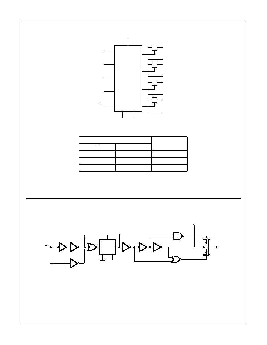
Pinout
CD74HC4316, CD74HCT4316
(PDIP, SOIC)
TOP VIEW
Ordering Information
PART NUMBER
TEMP. RANGE
(
o
C)
PACKAGE
PKG.
NO.
CD74HC4316E
-55 to 125
16 Ld PDIP
E16.3
CD74HCT4316E
-55 to 125
16 Ld PDIP
E16.3
CD74HC4316M
-55 to 125
16 Ld SOIC
M16.15
CD74HCT4316M
-55 to 125
16 Ld SOIC
M16.15
NOTES:
1. When ordering, use the entire part number. Add the suffix 96 to
obtain the variant in the tape and reel.
2. Wafer and die is available which meets all electrical
specifications. Please contact your local sales office or Harris
customer service for ordering information.
14
15
16
9
13
12
11
10
1
2
3
4
5
7
6
8
1Z
1Y
2Y
2Z
2S
3S
GND
E
V
CC
4S
4Z
4Y
3Y
3Z
V
EE
1S
February 1998
CAUTION: These devices are sensitive to electrostatic discharge. Users should follow proper IC Handling Procedures.
Copyright
©
Harris Corporation 1998
File Number
1916.1
[ /Title
(CD74
HC431
6,
CD74
HCT43
16)
/Sub-
ject
(High-
Speed
CMOS
2
Functional Diagram
TRUTH TABLE
INPUTS
SWITCH
E
S
L
L
OFF
L
H
ON
H
X
OFF
NOTE:
H = High Level Voltage
L
= Low Level Voltage
X = Don't Care
15
5
14
6
4S
3S
2S
1S
1Y
1Z
2Y
2Z
3Y
3Z
4Y
4Z
7
E
16
V
CC
8
9
V
EE
GND
2
1
3
4
11
10
12
13
LOGIC
LEVEL
CONV.
AND
CONTROL
Logic Diagram
FIGURE 1. ONE SWITCH
V
CC
V
EE
nZ
nY
E
LOGIC
LEVEL
CONV.
V
CC
V
EE
TO 3 OTHER
SWITCHES
nS
CD74HC4316, CD74HCT4316
CD74HC4316, CD74HCT4316

3
Absolute Maximum Ratings
Thermal Information
DC Supply Voltage, V
CC
. . . . . . . . . . . . . . . . . . . . . . . . -0.5V to 7V
DC Supply Voltage, V
CC -
V
EE
. . . . . . . . . . . . . . . . . . -0.5V to 10.5V
DC Supply Voltage, V
EE
. . . . . . . . . . . . . . . . . . . . . . . . 0.5V to -7V
DC Input Diode Current, I
IK
For V
I
< -0.5V or V
I
> V
CC
0.5V
. . . . . . . . . . . . . . . . . . . . . . . .±
20mA
DC Switch Diode Current, I
OK
For V
I
< V
EE
-0.5V or V
I
< V
CC
+ 0.5V
. . . . . . . . . . . . . . . . .±
25mA
DC Switch Diode Current
For V
I
> V
EE
-0.5V or V
I
< V
CC
+ 0.5V
. . . . . . . . . . . . . . . . .±
25mA
DC Output Diode Current, I
OK
For V
O
< -0.5V or V
O
> V
CC
+ 0.5V
. . . . . . . . . . . . . . . . . . . .±
20mA
DC Output Source or Sink Current per Output Pin, I
O
For V
O
> -0.5V or V
O
< V
CC
+ 0.5V
. . . . . . . . . . . . . . . . . . . .±
25mA
DC V
CC
or Ground Current, I
CC
. . . . . . . . . . . . . . . . . . . . . . . . .±
50mA
Operating Conditions
Temperature Range, T
A
. . . . . . . . . . . . . . . . . . . . . . -55
o
C to 125
o
C
Supply Voltage Range, V
CC
HC Types . . . . . . . . . . . . . . . . . . . . . . . . . . . . . . . . . . . . .2V to 6V
HCT Types . . . . . . . . . . . . . . . . . . . . . . . . . . . . . . . . .4.5V to 5.5V
Supply Voltage Range, V
CC -
V
EE
HC, HCT Types (Figure 2) . . . . . . . . . . . . . . . . . . . . . . .2V to 10V
Supply Voltage Range, V
EE
HC, HCT Types (Figure 3) . . . . . . . . . . . . . . . . . . . . . . . 0V to -6V
DC Input or Output Voltage, V
I
. . . . . . . . . . . . . . . . . . . GND to V
CC
Analog Switch I/O Voltage, V
IS
. . . . . . . . . . . . . . . . . . . . . V
EE
(Min)
. . . . . . . . . . . . . . . . . . . . . . . . . . . . . . . . . . . . . . . . . . . V
CC
(Max)
Input Rise and Fall Time, t
r
, t
f
2V . . . . . . . . . . . . . . . . . . . . . . . . . . . . . . . . . . . . . . 1000ns (Max)
4.5V. . . . . . . . . . . . . . . . . . . . . . . . . . . . . . . . . . . . . . 500ns (Max)
6V . . . . . . . . . . . . . . . . . . . . . . . . . . . . . . . . . . . . . . . 400ns (Max)
Thermal Resistance (Typical, Note 3)
JA
(
o
C/W)
PDIP Package . . . . . . . . . . . . . . . . . . . . . . . . . . . . .
90
SOICSC Package . . . . . . . . . . . . . . . . . . . . . . . . . .
115
Maximum Junction Temperature (Plastic Package) . . . . . . . . 150
o
C
Maximum Storage Temperature Range . . . . . . . . . .-65
o
C to 150
o
C
Maximum Lead Temperature (Soldering 10s) . . . . . . . . . . . . . 300
o
C
CAUTION: Stresses above those listed in "Absolute Maximum Ratings" may cause permanent damage to the device. This is a stress only rating and operation
of the device at these or any other conditions above those indicated in the operational sections of this specification is not implied.
NOTE:
3.
JA
is measured with the component mounted on an evaluation PC board in free air.
Recommended Operating Area as a Function of Supply Voltage
FIGURE 2.
FIGURE 3.
8
6
4
2
0
V
CC
- GND
(V)
HC
HCT
0
2
4
6
8
10 12
V
CC
- V
EE
(V)
8
6
4
2
0
V
CC
- GND
(V)
HC
HCT
0
-2
-4
-6
-8
V
EE
- GND (V)
CD74HC4316, CD74HCT4316
CD74HC4316, CD74HCT4316

4
DC Electrical Specifications
PARAMETER
SYMBOL
TEST CONDITIONS
25
o
C
-40
o
C TO
85
o
C
-55
o
C TO
125
o
C
UNITS
V
I
(V)
V
IS
(V)
V
EE
(V)
V
CC
(V)
MIN
TYP
MAX
MIN
MAX
MIN
MAX
HC TYPES
High Level Input
Voltage
V
IH
-
-
-
2
1.5
-
-
1.5
-
1.5
-
V
4.5
3.15
-
-
3.15
-
3.15
-
V
6
4.2
-
-
4.2
-
4.2
-
V
Low Level Input
Voltage
V
IL
-
-
-
2
-
-
0.5
-
0.5
-
0.5
V
4.5
-
-
1.35
-
1.35
-
1.35
V
6
-
-
1.8
-
1.8
-
1.8
V
"ON" Resistance
I
O
= 1mA
Figure 4, 5
R
ON
V
IH
or
V
IL
V
CC
or
V
EE
0
4.5
-
45
180
-
225
-
270
0
6
-
35
160
-
200
-
240
-4.5
4.5
-
30
135
-
170
-
205
V
CC
to
V
EE
0
4.5
-
85
320
-
400
-
480
0
6
-
55
240
-
300
-
360
-4.5
4.5
-
35
170
-
215
-
255
Maximum "ON"
Resistance Between
Any Two Channels
R
ON
-
-
0
4.5
-
10
-
-
-
-
-
0
6
-
8.5
-
-
-
-
-
-4.5
4.5
-
5
-
-
-
-
-
Switch Off Leakage
Current
I
IZ
V
IH
or
V
IL
V
CC
-
V
EE
0
6
-
-
±
0.1
-
±
1
-
±
1
µ
A
-5
5
-
-
±
0.1
-
±
1
-
±
1
µ
A
Control Input Leakage
Current
I
IL
V
CC
or
GND
-
0
6
-
-
±
0.1
-
±
1
-
±
1
µ
A
Quiescent Device
Current
I
O
= 0
I
CC
V
CC
or
GND
When
V
IS
= V
EE
,
V
OS
=V
CC
When
V
IS
= V
CC
,
V
OS
=V
EE
0
6
-
-
8
-
80
-
160
µ
A
-5
5
-
-
16
-
160
-
320
µ
A
HCT TYPES
High Level Input
Voltage
V
IH
-
-
-
4.5 to
5.5
2
-
-
2
-
2
-
V
Low Level Input
Voltage
V
IL
-
-
-
4.5 to
5.5
-
-
0.8
-
0.8
-
0.8
V
"ON" Resistance
I
O
= 1mA
Figure 4, 5
R
ON
V
IH
or
V
IL
V
CC
or
V
EE
0
4.5
-
45
180
-
225
-
270
-4.5
4.5
-
30
135
-
170
-
205
V
CC
to
V
EE
0
4.5
-
85
320
-
400
-
480
-4.5
4.5
-
35
170
-
215
-
255
Maximum "ON"
Resistance Between
Any Two Channels
R
ON
-
-
0
4.5
-
10
-
-
-
-
-
-4.5
4.5
-
5
-
-
-
-
-
Switch Off Leakage
Current
I
IZ
V
IH
or
V
IL
V
CC
-
V
EE
0
6
-
-
±
0.1
-
±
1
-
±
1
µ
A
-5
5
-
-
±
0.1
-
±
1
-
±
1
µ
A
CD74HC4316, CD74HCT4316
CD74HC4316, CD74HCT4316

5
Control Input Leakage
Current
I
I
V
CC
or
GND
-
0
5.5
-
-
±
0.1
-
±
1
-
±
1
µ
A
Quiescent Device
Current
I
O
= 0
I
CC
Any
Voltage
Be-
tween
V
CC
and
GND
When
V
IS
= V
EE
,
V
OS
=
V
CC
,
When
V
IS
= V
CC
,
V
OS
= V
EE
0
5.5
-
-
8
-
80
-
160
µ
A
-4.5
5.5
-
-
16
-
160
-
320
µ
A
Additional Quiescent
Device Current Per
Input Pin: 1 Unit Load
I
CC
V
CC
-2.1
-
-
4.5 to
5.5
-
100
360
-
450
-
490
µ
A
NOTE: For dual-supply systems theoretical worst case (V
I
= 2.4V, V
CC
= 5.5V) specification is 1.8mA.
HCT Input Loading Table
INPUT
UNIT LOADS
All
0.5
NOTE: Unit Load is
I
CC
limit specified in DC Electrical Table, e.g.,
360
µ
A max at 25
o
C.
DC Electrical Specifications
(Continued)
PARAMETER
SYMBOL
TEST CONDITIONS
25
o
C
-40
o
C TO
85
o
C
-55
o
C TO
125
o
C
UNITS
V
I
(V)
V
IS
(V)
V
EE
(V)
V
CC
(V)
MIN
TYP
MAX
MIN
MAX
MIN
MAX
Switching Specifications
Input t
r
, t
f
= 6ns
PARAMETER
SYMBOL
TEST
CONDITIONS
V
EE
(V)
V
CC
(V)
25
o
C
-40
o
C TO
85
o
C
-55
o
C TO
125
o
C
UNITS
MIN
TYP
MAX
MIN
MAX
MIN
MAX
HC TYPES
Propagation Delay,
Switch In to Out
t
PLH
, t
PHL
C
L
= 50pF
0
2
-
-
60
-
75
-
90
ns
0
4.5
-
-
12
-
15
-
18
ns
0
6
-
-
10
-
13
-
15
ns
-4.5
4.5
-
-
8
-
10
-
12
ns
Turn "ON" Time E to Out
t
PZH
, t
PZL
C
L
= 50pF
0
2
-
-
205
-
255
-
310
ns
0
4.5
-
-
41
-
51
-
62
ns
0
6
-
-
35
-
43
-
53
ns
-4.5
4.5
-
-
37
-
47
-
56
ns
C
L
= 15pF
-
5
-
17
-
-
-
-
-
ns
Turn "ON" Time nS to Out
t
PZH
, t
PZL
C
L
= 50pF
0
2
-
-
175
-
220
-
265
ns
0
4.5
-
-
35
-
44
-
53
ns
0
6
-
-
30
-
37
-
45
ns
-4.5
4.5
-
-
34
-
43
-
51
ns
C
L
= 15pF
-
5
-
14
-
-
-
-
-
ns
Turn "OFF" Time E to Out
t
PLZ,
t
PHZ
C
L
= 50pF
0
2
-
-
205
-
255
-
310
ns
0
4.5
-
-
41
-
51
-
62
ns
0
6
-
-
35
-
43
-
53
ns
-4.5
4.5
-
-
37
-
47
-
56
ns
C
L
= 15pF
-
5
-
17
-
-
-
-
-
ns
CD74HC4316, CD74HCT4316
CD74HC4316, CD74HCT4316