
HCC/HCF40109B
QUAD LOW-TO-HIGH VOLTAGE LEVEL SHIFTER
DESCRIPTION
.
INDEPENDENCE OF POWER SUPPLY SE-
QUENCE CONSIDERATIONS V
CC
CAN EX-
CEED V
DD
, INPUT SIGNALS CAN EXCEED
BOTH V
CC
AND V
DD
.
UP AND DOWN LEVEL-SHIFTING CAPA-
BILITY
.
THREE-STATE OUTPUTS WITH SEPARATE
ENABLE CONTROLS
.
STANDARDIZED
SYMMETRICAL
OUTPUT
CHARACTERISTICS
.
QUIESCENT CURRENT SPECIFIED AT 20V
FOR HCC DEVICE
.
5V, 10V, AND 15V PARAMETRIC RATINGS
.
INPUT CURRENT OF 100nA AT 18V AND 25
°
C
FOR HCC DEVICE
.
100% TESTED FOR QUIESCENT CURRENT
.
MEETS ALL REQUIREMENTS OF JEDEC TEN-
TATIVE STANDARD N
°
. 13A, "STANDARD
SPECIFICATIONS FOR DESCRIPTION OF "B"
SERIES CMOS DEVICES"
June 1989
The HCC40109B (extended temperature range)
and HCF40109B (intermediate temperature range)
are monolithic integrated circuits, available in 16-
lead dual in-line plastic or ceramic package and
plastic micropackage. The HCC/HCF40109B con-
tains four low-to-high-voltage level-shifting circuits.
Each circuit will shift a low-voltage digital-logic input
signal (A, B, C, D) with logical 1 = V
CC
and logical 0
= V
SS
to a higher-voltage output signal (E, F, G, H)
with logical 1 = V
DD
and logical 0 = V
SS
. The
HCC/HCF40109B, unlike other low-to-high level-
shifting circuits, does not require the presence of the
high-voltage supply (V
DD
) before the application of
either the low-voltage supply (V
CC
) or the input sig-
nals. There are no restrictions on the sequence of
application of V
DD
, V
CC
, or the input signals. In ad-
dition, there are no restrictions on the relative mag-
nitudes od the supply voltages or input signals within
the device maximum ratings ; V
CC
may exceed V
DD
,
and input signals may exceed V
CC
, and V
DD
. When
operated
in
the
mode
V
CC
V
DD
,
the
HCC/HCF40109B, will operate as a high-to-low
level-shifter. The HCC/HCF 40109B also features
individual three-state output capability. A low level
on any of the separately enabled three-state output
EY
(Plastic Package)
F
(Ceramic Frit Seal Package)
C1
(Plastic Chip Carrier)
ORDER CODES :
HCC40109BF
HCF40109BM1
HCF40109BEY
HCF40109BC1
PIN CONNECTIONS
controls produces a high-impedance state in the
corresponding output.
C1
(Micro package)
1/12

FUNCTIONAL DIAGRAM
ABSOLUTE MAXIMUM RATINGS
Symbol
Parameter
Value
Unit
V
DD
*
Supply Voltage : HC C Types
H C F Types
0.5 to + 20
0.5 to + 18
V
V
V
i
Input Voltage
0.5 to V
DD
+ 0.5
V
I
I
DC Input Current (any one input)
±
10
mA
P
t o t
Total Power Dissipation (per package)
Dissipation per Output Transistor
for T
o p
= Full Package-temperature Range
200
100
mW
mW
T
o p
Operating Temperature : HCC Types
H CF Types
55 to + 125
40 to + 85
°
C
°
C
T
s t g
Storage Temperature
65 to + 150
°
C
RECOMMENDED OPERATING CONDITIONS
Symbol
Parameter
Value
Unit
V
DD
Supply Voltage : H CC Types
H C F Types
3 to 18
3 to 15
V
V
V
I
Input Voltage
0 to V
DD
V
T
o p
Operating Temperature : HCC Types
H CF Types
55 to + 125
40 to + 85
°
C
°
C
Stresses above those listed under "Absolute Maximum Ratings" may cause permanent damage to the device. This is a stress rating only
and functional operation of the device at these or any other conditions above those indicated in the operational sections of this specification
is not implied. Exposure to absolute maximum rating conditions for external periods may affect device reliability.
* All voltage are with respect to V
SS
(GND).
LOGIC DIAGRAM
Inputs
Outputs
Mode
A, B, C , D
E nable
A, B, C , D E , F , G , H
Low to High
Level Shift
0
1
0
1
1
1
X
0
Z
LOGIC 0 = LOW (V
SS
)
X = Don't Care.
Z = High Impedance.
LOGIC 1 = V
CC
at INPUTS and V
DD
at OUTPUTS.
1 of 4 units
TRUTH TABLE
HCC/HCF40109B
2/12

STATIC ELECTRICAL CHARACTERISTICS (over recommended operating conditions)
Test Conditions
Value
T
L o w
*
25
°
C
T
Hig h
*
Symbol
Parameter
V
I
(V)
V
O
(V)
|I
O
|
(
µ
A)
V
CC
(V)
V
DD
(V)
Min
Max.
Min.
Typ.
Max.
Min.
Max.
Unit
I
L
Quiescent
Current
HCC
Types
0/ 5
5
1
0.02
1
30
0/10
10
2
0.02
2
60
0/15
15
4
0.02
4
120
µ
A
0/20
20
20
0.04
20
600
HCF
Types
0/ 5
5
4
0.02
4
30
0/10
10
8
0.02
8
60
0/15
15
16
0.02
16
120
V
OH
Output High
Voltage
0/ 5
< 1
5
4.95
4.95
4.95
V
0/10
< 1
10
9.95
9.95
9.95
0/15
< 1
15
14.95
14.95
14.95
V
OL
Output Low
Voltage
5/0
< 1
5
0.05
0.05
0.05
V
10/0
< 1
10
0.05
0.05
0.05
15/0
< 1
15
0.05
0.05
0.05
V
IH
Input High Voltage
1/9
< 1
5
10
3.5
3.5
3.5
V
1.5/13.5
< 1
10
15
7
7
7
V
IL
Input Low Voltage
1/9
< 1
5
10
1.5
1.5
1.5
V
1.5/13.5
< 1
10
15
3
3
3
I
OH
Output
Drive
Current
HCC
Types
0/ 5
2.5
5
2
1.6
3.2
1.15
mA
0/ 5
4.6
5
0.64
0.51
1
0.36
0/10
9.5
10
1.6
1.3
2.6
0.9
0/15
13.5
15
4.2
3.4
6.8
2.4
HCF
Types
0/ 5
2.5
5
1.53
1.36 3.2
1.1
0/ 5
4.6
5
0.52
0.44
1
0.36
0/10
9.5
10
1.3
1.1
2.6
0.9
0/15
13.5
15
3.6
3.0
6.8
2.4
I
OL
Output
Sink
Current
HCC
Types
0/ 5
0.4
5
0.64
0.51
1
0.36
mA
0/10
0.5
10
1.6
1.3
2.6
0.9
0/15
1.5
15
4.2
3.4
6.8
2.4
HCF
Types
0/ 5
0.4
5
0.52
0.44
1
0.36
0/10
0.5
10
1.3
1.1
2.6
0.9
0/15
1.5
15
3.6
3.0
6.8
2.4
I
IH
, I
IL
Input
Leakage
Current
HCC
Types
0/18
18
±
0.1
±
10
-5
±
0.1
±
1
µ
A
Any Input
HCF
Types
0/15
15
±
0.3
±
10
-5
±
0.3
±
1
* T
Low
= 55
°
C for HCC device : 40
°
C for HCF device.
* T
High
= + 125
°
C for HCC device : + 85
°
C for HCF device.
The Noise Margin for both "1" and "0" level is : 1V min. with V
DD
= 5V, 2V min. with V
DD
= 10V, 2.5V min. with V
DD
= 15V.
** Forced output disabled.
HCC/HCF40109B
3/12

DYNAMIC ELECTRICAL CHARACTERISTICS (T
amb
= 25
°
C, C
L
= 50pF, R
L
= 200k
,
typical temperature coefficient for all V
DD
values is 0.3%/
°
C, all input rise and fall time = 20ns)
Test Conditions
Value
Symbol
Parameter
Shifting Mode
V
CC
(V) V
DD
(V)
Min.
Typ.
Max.
Unit
t
PHL
,
t
PLH
Propagation Delay Time
(data input to output)
High to Low Level
L - H
5
10
300
600
ns
5
15
220
440
10
15
180
360
H - L
10
5
850
1600
15
5
850
1600
15
10
290
580
Low to High Level
L - H
5
10
130
260
ns
5
15
120
240
10
15
70
140
H - L
10
5
230
460
15
5
230
460
15
10
80
160
t
PHZ
3-State Disable Delay Time
Output High to High Impedance
L - H
5
10
60
120
ns
5
15
50
100
10
15
35
70
H - L
10
5
120
240
15
5
120
240
15
10
40
80
t
PZ H
High Impedance to Output High
L - H
5
10
320
640
ns
5
15
230
460
10
15
180
360
H - L
10
5
800
1500
15
5
800
1500
15
10
280
560
t
PLZ
Output Low to High Impedance
L - H
5
10
370
740
ns
5
15
300
600
10
15
250
500
H - L
10
5
850
1600
15
5
850
1600
15
10
350
700
STATIC ELECTRICAL CHARACTERISTICS (continued)
Test Conditions
Value
V
I
V
O
I
O
V
CC
V
DD
T
L ow
*
25
°
C
T
Hig h
*
Symbol
Parameter
(V)
(V)
(V)
(V)
(V)
Min.
Max.
Min.
Typ.
Max.
Min.
Max.
Unit
I
OH
,
I
OL
**
3-State
Output
Leakage
Current
HCC
Types
0/18
0/18
18
±
0.4
±
10
- 4
±
0.4
±
12
µ
A
HCF
Types
0/15
0/15
15
±
1.0
±
10
- 4
±
1.0
±
7.5
C
I
Input Capacitance
Any Input
5
7.5
pF
* T
Low
= 55
°
C for HCC device : 40
°
C for HCF device.
* T
High
= + 125
°
C for HCC device : + 85
°
C for HCF device.
The Noise Margin for both "1" and "0" level is : 1V min. with V
DD
= 5V, 2V min. with V
DD
= 10V, 2.5V min. with V
DD
= 15V.
** Forced output disabled.
HCC/HCF40109B
4/12

DYNAMIC ELECTRICAL CHARACTERISTICS (continued)
Test Conditions
Value
Symbol
Parameter
Shifting Mode
V
CC
(V) V
DD
(V)
Min.
Typ.
Max.
Unit
t
PZL
High Impedance to Output Low
L - H
5
10
100
200
ns
5
15
80
160
10
15
40
80
H - L
10
5
120
240
15
5
120
240
15
10
40
80
t
T HL
,
t
T LH
Transition Time
L - H
5
10
50
100
ns
5
15
40
80
10
15
40
80
H - L
10
5
100
200
15
5
100
200
15
10
50
100
Output Low (sink) Current Characteristics.
Output High (source) Current Characteristics.
Typical Transition Timevs. Load Capacitance.
Typical High-to-low Propagation Delay Time vs.
Load Capacitance.
HCC/HCF40109B
5/12

Typical Input Switching vs. High-level Supply Volt-
age.
Typical Low-to-high Propagation Delay Time vs.
Load Capacitance.
TEST CIRCUITS
Output Enable Delay Times Test Circuit and Waveforms.
High-level Supply Voltage vs. Low-level Supply
Voltage.
Typical Dynamic Power Dissipation vs. Input Fre-
quency.
HCC/HCF40109B
6/12

Input Leakage Current.
Dynamic Power Dissipation.
TEST CIRCUITS (continued)
Quiescent Device Current.
Input Voltage.
HCC/HCF40109B
7/12

Plastic DIP16 (0.25) MECHANICAL DATA
DIM.
mm
inch
MIN.
TYP.
MAX.
MIN.
TYP.
MAX.
a1
0.51
0.020
B
0.77
1.65
0.030
0.065
b
0.5
0.020
b1
0.25
0.010
D
20
0.787
E
8.5
0.335
e
2.54
0.100
e3
17.78
0.700
F
7.1
0.280
I
5.1
0.201
L
3.3
0.130
Z
1.27
0.050
P001C
HCC/HCF40109B
8/12

Ceramic DIP16/1 MECHANICAL DATA
DIM.
mm
inch
MIN.
TYP.
MAX.
MIN.
TYP.
MAX.
A
20
0.787
B
7
0.276
D
3.3
0.130
E
0.38
0.015
e3
17.78
0.700
F
2.29
2.79
0.090
0.110
G
0.4
0.55
0.016
0.022
H
1.17
1.52
0.046
0.060
L
0.22
0.31
0.009
0.012
M
0.51
1.27
0.020
0.050
N
10.3
0.406
P
7.8
8.05
0.307
0.317
Q
5.08
0.200
P053D
HCC/HCF40109B
9/12

SO16 (Narrow) MECHANICAL DATA
DIM.
mm
inch
MIN.
TYP.
MAX.
MIN.
TYP.
MAX.
A
1.75
0.068
a1
0.1
0.2
0.004
0.007
a2
1.65
0.064
b
0.35
0.46
0.013
0.018
b1
0.19
0.25
0.007
0.010
C
0.5
0.019
c1
45
°
(typ.)
D
9.8
10
0.385
0.393
E
5.8
6.2
0.228
0.244
e
1.27
0.050
e3
8.89
0.350
F
3.8
4.0
0.149
0.157
G
4.6
5.3
0.181
0.208
L
0.5
1.27
0.019
0.050
M
0.62
0.024
S
8
°
(max.)
P013H
HCC/HCF40109B
10/12
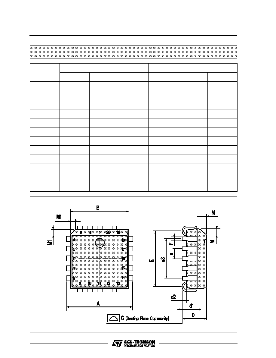
PLCC20 MECHANICAL DATA
DIM.
mm
inch
MIN.
TYP.
MAX.
MIN.
TYP.
MAX.
A
9.78
10.03
0.385
0.395
B
8.89
9.04
0.350
0.356
D
4.2
4.57
0.165
0.180
d1
2.54
0.100
d2
0.56
0.022
E
7.37
8.38
0.290
0.330
e
1.27
0.050
e3
5.08
0.200
F
0.38
0.015
G
0.101
0.004
M
1.27
0.050
M1
1.14
0.045
P027A
HCC/HCF40109B
11/12

Information furnished is believed to be accurate and reliable. However, SGS-THOMSON Microelectronics assumes no responsability for the
consequences of use of such information nor for any infringement of patents or other rights of third parties which may results from its use. No
license is granted by implication or otherwise under any patent or patent rights of SGS-THOMSON Microelectronics. Specifications mentioned
in this publication are subject to change without notice. This publication supersedes and replaces all information previously supplied.
SGS-THOMSON Microelectronics products are not authorized for use as critical components in life support devices or systems without express
written approval of SGS-THOMSON Microelectonics.
©
1994 SGS-THOMSON Microelectronics - All Rights Reserved
SGS-THOMSON Microelectronics GROUP OF COMPANIES
Australia - Brazil - France - Germany - Hong Kong - Italy - Japan - Korea - Malaysia - Malta - Morocco - The Netherlands -
Singapore - Spain - Sweden - Switzerland - Taiwan - Thailand - United Kingdom - U.S.A
HCC/HCF40109B
12/12