
HCC40105B
HCF40105B
FIFO REGISTER
DESCRIPTION
.
INDEPENDENT ASYNCHRONOUS INPUTS
AND OUTPUTS
.
3-STATE OUTPUTS
.
EXPANDABLE IN EITHER DIRECTION
.
STATUS INDICATORS ON INPUT AND OUT-
PUT
.
RESET CAPABILITY
.
STANDARDIZED, SYMMETRICAL OUTPUT
CHARACTERISTICS
.
QUIESCENT CURRENT SPECIFIED AT 20V
FOR HCC DEVICE
.
5V, 10V, AND 15V PARAMETRIC RATINGS
.
INPUT CURRENT OF 100nA AT 18V AND 25
°
C
FOR HCC DEVICE
.
100% TESTED FOR QUIESCENT CURRENT
.
MEETS ALL REQUIREMENTS OF JEDEC TEN-
TATIVE STANDARD N
o
13A, "STANDARD
SPECIFICATIONS FOR DESCRIPTION OF "B"
SERIES CMOS DEVICES"
June 1989
The HCC40105B (extended temperature range) and
HCF40105B (intermediate temperature range) are
monolithic integrated circuits, available in 16-lead dual
in-line plastic or ceramic package.
The HCC/HCF40105B is a low-power first-in-first-out
(FIFO) "elastic" storage register that can store 16 4-bit
words. It is capable of handling input and output data
at different shifting rates. This feature makes it particu-
larly useful as a buffer between asynchronous sys-
tems. Each word position in the register is clocked by
a control flip-flop, which stores a marker bit. A "1" sig-
nifies that the position's data is filled and a "0" denotes
a vacancy in that position. The control flip-flop detects
the state of the preceding flip-flop and communicates
its own status to the succeeding flip-flop. When a con-
trol flip-flop is in the "0" state and sees a "1" in the
preceding flip-flop, it generates a clock pulse that
transfers data from the preceding four data latches
into its own four data latches and resets the preceding
flip-flop to "0". The first and last control flip-flops have
buffered outputs. Since all empty locations "bubble"
automatically to the input end, and all valid data ripple
through to the output end, the status of the first control
flip-flop (DATA-IN READY) indicates if the FIFO is full,
and the status of the last flip-flop (DATA-OUT
EY
(Plastic Package)
F
(Ceramic Package)
C1
(Chip Carrier)
ORDER CODES :
HCC40105BF
HCF40105BEY
HCF40105BC1
PIN CONNECTIONS
READY) indicates if the FIFO contains data. As the
earliest data are removed from the bottom of the data
stack (the output end), all data entered later will auto-
matically propagate (ripple) toward the output.
1/12

FUNCTIONAL DIAGRAM
ABSOLUTE MAXIMUM RATINGS
Symbol
Parameter
Value
Unit
V
DD
*
Supply Voltage : HCC Types
HC F Types
0.5 to + 20
0.5 to + 18
V
V
V
i
Input Voltage
0.5 to V
DD
+ 0.5
V
I
I
DC Input Current (any one input)
±
10
mA
P
t o t
Total Power Dissipation (per package)
Dissipation per Output Transistor
for T
o p
= Full Package-temperature Range
200
100
mW
mW
T
o p
Operating Temperature : H CC Types
H C F Types
55 to + 125
40 to + 85
°
C
°
C
T
s t g
Storage Temperature
65 to + 150
°
C
RECOMMENDED OPERATING CONDITIONS
Symbol
Parameter
Value
Unit
V
DD
Supply Voltage : HC C Types
H CF Types
3 to 18
3 to 15
V
V
V
I
Input Voltage
0 to V
DD
V
T
o p
Operating Temperature : H CC Types
H C F Types
55 to + 125
40 to + 85
°
C
°
C
Stresses above those listed under "Absolute Maximum Ratings" may cause permanent damage to the device. This is a stress rating
only and functional operation of the device at these or any other conditions above those indicated in the operational sections of this
specification is not implied. Exposure to absolute maximum rating conditions for external periods may affect device reliability.
* All voltage values are referred to V
SS
pin voltage.
HCC/HCF40105B
2/12

LOGIC DIAGRAM
TIMING DIAGRAM
HCC/HCF40105B
3/12

STATIC ELECTRICAL CHARACTERISTICS (over recommended operating conditions)
Test Conditions
Value
V
I
V
O
|I
O
|
V
D D
T
L o w
*
25
°
C
T
Hi g h
*
Symbol
Parameter
(V)
(V)
(
µ
A)
(V)
Min. Max. Min. Typ. Max. Min. Max.
Unit
I
L
Quiescent
Current
HCC
Types
0/ 5
5
5
0.04
5
150
µ
A
0/10
10
10
0.04
10
300
0/15
15
20
0.04
20
600
0/20
20
100
0.08
100
3000
HCF
Types
0/ 5
5
20
0.04
20
150
0/10
10
40
0.04
40
300
0/15
15
80
0.04
80
600
V
O H
Output High
Voltage
0/ 5
< 1
5
4.95
4.95
4.95
V
0/10
< 1
10
9.95
9.95
9.95
0/15
< 1
15
14.95
14.95
14.95
V
O L
Output Low
Voltage
5/0
< 1
5
0.05
0.05
0.05
V
10/0
< 1
10
0.05
0.05
0.05
15/0
< 1
15
0.05
0.05
0.05
V
IH
Input High
Voltage
0.5/4.5
< 1
5
3.5
3.5
3.5
V
1/9
< 1
10
7
7
7
1.5/13.5
< 1
15
11
11
11
V
IL
Input Low
Voltage
4.5/0.5
< 1
5
1.5
1.5
1.5
V
9/1
< 1
10
3
3
3
13.5/1.5
< 1
15
4
4
4
I
O H
Output
Drive
Current
HCC
Types
0/ 5
2.5
5
2
1.6 3.2
1.15
mA
0/ 5
4.6
5
0.64
0.51 1
0.36
0/10
9.5
10
1.6
1.3 2.6
0.9
0/15
13.5
15
4.2
3.4 6.8
2.4
HCF
Types
0/ 5
2.5
5
1.53
1.36 3.2
1.1
0/ 5
4.6
5
0.52
0.44 1
0.36
0/10
9.5
10
1.3
1.1 2.6
0.9
0/15
13.5
15
3.6
3.0 6.8
2.4
I
O L
Output
Sink
Current
HCC
Types
0/ 5
0.4
5
0.64
0.51
1
0.36
mA
0/10
0.5
10
1.6
1.3
2.6
0.9
0/15
1.5
15
4.2
3.4
6.8
2.4
HCF
Types
0/ 5
0.4
5
0.52
0.44
1
0.36
0/10
0.5
10
1.3
1.1
2.6
0.9
0/15
1.5
15
3.6
3.0
6.8
2.4
I
IH
, I
IL
Input
Leakage
Current
HCC
Types
0/18
Any Input
18
±
0.1
±
10
5
±
0.1
±
1
µ
A
HCF
Types
0/15
15
±
0.3
±
10
5
±
0.3
±
1
I
O H
,I
O L
**
3-State
Output
Leakage
Current
HCC
Types
0/18
0/18
18
±
0.4
±
10
4
±
0.4
±
12
µ
A
HCF
Types
0/15
0/15
15
±
1.0
±
10
4
±
1.0
±
7.5
C
I
Input Capacitance
Any Input
5
7.5
pF
*
T
Lo w
=
55
°
C for HCC device : 40
°
C for HCF device.
*
T
High
= + 125
°
C for HCC device : + 85
°
C for HCF device.
The Noise Margin for both "1" and "0" level is : 1V min. with V
DD
= 5V, 2V min. with V
DD
= 10V, 2.5 V min. with V
DD
= 15V.
* * Forced output disable.
HCC/HCF40105B
4/12

DYNAMIC ELECTRICAL CHARACTERISTICS (T
amb
= 25
°
C, C
L
= 50 pF, R
L
= 200 k
,
typical temperature coefficient for all V
D D
values is 0.3 %/
°
C, all input rise and fall time = 20 ns)
Test Conditions
Value
Symbol
Parameter
V
D D
(V) Min.
Typ.
Max.
Unit
t
P HL
Propagation Delay Time
Shift-out or Reset to Data-out
Ready
5
185
370
ns
10
90
180
15
65
130
t
P HL
Propagation Delay Time
Shift-in to Data-in Ready
5
160
320
ns
10
65
130
15
45
90
t
P ZH
, t
P ZL
Propagation Delay Time
3-state Control to Data-out
5
140
280
ns
10
60
120
15
40
80
t
P HZ
, t
P L Z
Propagation Delay Time
3-State Control to Data-out
5
100
200
ns
10
50
100
15
40
80
t
P L H
Ripple-through Delay Input to
Output
5
2
4
µ
s
10
1
2
15
0.7
1.4
t
THL
, t
TL H
Transition Time
5
100
200
ns
10
50
100
15
40
80
f
I
Shift-in or Shift-out Rate
5
1.5
3
MHz
10
3
6
15
4
8
t
WH
Shift-in Pulse Width
5
200
100
ns
10
80
40
15
60
30
t
WL
Shift-out Pulse Width
5
360
180
ns
10
160
80
15
100
50
t
r
Shift-in or Shift-out Rise Time
5
15
µ
s
10
15
15
15
t
f
Shift-in Fall Time
5
15
µ
s
10
15
15
15
t
f
Shift-out Fall Time
5
15
µ
s
10
5
15
5
t
s e t u p
Data Setup Time
5
0
ns
10
0
15
0
HCC/HCF40105B
5/12

Output Low (sink) Current Characteristics.
Output High (source) Current Characteristics.
Typical Transition Time vs. Load Capacitance.
Typical Dynamic Power Dissipation vs. Fre-
quency.
DYNAMIC ELECTRICAL CHARACTERISTICS (continued)
Test Conditions
Val ue
Symbol
Parameter
V
D D
(V)
Min.
Typ.
Max.
Unit
t
h o ld
Data Hold Time
5
350
175
ns
10
150
75
15
120
60
t
WL
Datain Ready Pulse Width
5
260
520
ns
10
100
120
15
70
140
t
WL
Dataout Ready Pulse Width
5
220
440
ns
10
90
180
15
665
130
t
WH
Master Reset Pulse Width
5
200
100
ns
10
90
45
15
60
30
HCC/HCF40105B
6/12
TYPICAL APPLICATIONS
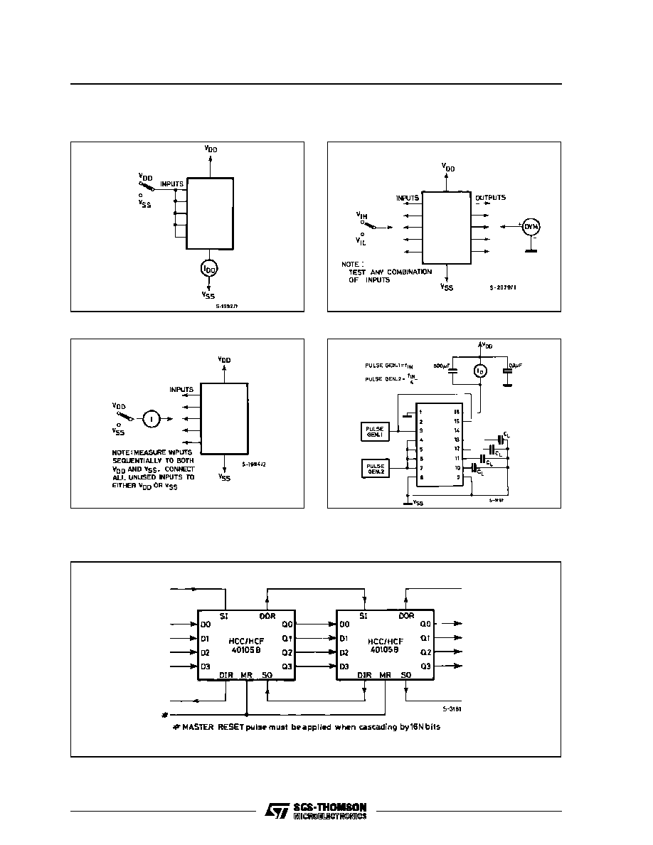
EXPANSION, 4 BITSWIDEBY16 NBITS LONG.
Input Leakage Current.
Dynamic Power Dissipation.
TEST CIRCUITS
Quiescent Device Current.
Input Voltage.
HCC/HCF40105B
7/12

LOADING DATA
Data can be entered whenever the DATA-IN READY
(DIR) flag is high, by a low to high transition on the
SHIFT-IN (SI) input. This input must go low momen-
tarily before the next word is accepted by the FIFO.
The DIR flag will go low momentarily, until the data
have been transferred tothe second location. The flag
will remain low when all 16-word locations are filled
with valid data, and further pulses on the SI input will
be ignored until DIR goes high.
UNLOADING DATA
As soon as the first word has rippled to the output,
DATA-OUT READY (DOR) goes high, and data can
be removed by afalling edge on theSO input. This fall-
ing edge causes the DOR signal to go low while the
word on the output is dumped and the next word
moves to the output. As long as valid data are avail-
able in the FIFO, the DOR signal will go high again sig-
nifying that the next word is ready at the output. When
the FIFO is empty, DOR will remain low, and any fur-
ther commands will be ignored until a "1" marker
ripples down to the last control register, when DOR
goes high. Unloading of data is inhibited while the 3-
state control input is high. The 3-state control signal
should not be shifted from high to low (data outputs
turned on)while the SHIFT-OUT is at logic 0. This level
change would cause the first word to be shifted out
(unloaded) immediately and the data to be lost.
CASCADING
The HCC/HCF40105B can be cascaded to form
longer registers simply by connecting the DIR to SO
and DOR to SI. In the cascaded mode, a MASTER
RESET pulse must be applied after the supply voltage
is turned on. For words wider than 4 bits, the DIR and
the DOR outputs must be gated together with AND
gates. Their outputs drive the SI and SO inputs in par-
allel, if expanding is done in both directions.
3-STATE OUTPUTS
In order to facilitate data busing, 3-state outputs are
provided on the data output lines, while the load con-
dition of the register can be detected by the state of
the DOR output.
MASTER RESET
A high on the MASTER RESET (MR) sets all the con-
trol logic marker bits to "0". DOR goes low and DIR
goes high. The contents of the data register are not
changed, only declared invalid, and will be super-
seded when the first word is loaded.
APPLICATIONS INFORMATION
EXPANSION, 8 BITSWIDEBY16 NBITS LONG.
HCC/HCF40105B
8/12

Plastic DIP14 MECHANICAL DATA
DIM.
mm
inch
MIN.
TYP.
MAX.
MIN.
TYP.
MAX.
a1
0.51
0.020
B
1.39
1.65
0.055
0.065
b
0.5
0.020
b1
0.25
0.010
D
20
0.787
E
8.5
0.335
e
2.54
0.100
e3
15.24
0.600
F
7.1
0.280
I
5.1
0.201
L
3.3
0.130
Z
1.27
2.54
0.050
0.100
P001A
HCC/HCF40105B
9/12

Ceramic DIP14/1 MECHANICAL DATA
DIM.
mm
inch
MIN.
TYP.
MAX.
MIN.
TYP.
MAX.
A
20
0.787
B
7.0
0.276
D
3.3
0.130
E
0.38
0.015
e3
15.24
0.600
F
2.29
2.79
0.090
0.110
G
0.4
0.55
0.016
0.022
H
1.17
1.52
0.046
0.060
L
0.22
0.31
0.009
0.012
M
1.52
2.54
0.060
0.100
N
10.3
0.406
P
7.8
8.05
0.307
0.317
Q
5.08
0.200
P053C
HCC/HCF40105B
10/12

PLCC20 MECHANICAL DATA
DIM.
mm
inch
MIN.
TYP.
MAX.
MIN.
TYP.
MAX.
A
9.78
10.03
0.385
0.395
B
8.89
9.04
0.350
0.356
D
4.2
4.57
0.165
0.180
d1
2.54
0.100
d2
0.56
0.022
E
7.37
8.38
0.290
0.330
e
1.27
0.050
e3
5.08
0.200
F
0.38
0.015
G
0.101
0.004
M
1.27
0.050
M1
1.14
0.045
P027A
HCC/HCF40105B
11/12

Information furnished is believed to be accurate and reliable. However, SGS-THOMSON Microelectronics assumes no responsability for the
consequences of use of such information nor for any infringement of patents or other rights of third parties which may results from its use. No
license is granted by implication or otherwise under any patent or patent rights of SGS-THOMSON Microelectronics. Specifications mentioned
in this publication are subject to change without notice. This publication supersedes and replaces all information previously supplied.
SGS-THOMSON Microelectronics products are not authorized for use as critical components in life support devices or systems without express
written approval of SGS-THOMSON Microelectonics.
©
1994 SGS-THOMSON Microelectronics - All Rights Reserved
SGS-THOMSON Microelectronics GROUP OF COMPANIES
Australia - Brazil - France - Germany - Hong Kong - Italy - Japan - Korea - Malaysia - Malta - Morocco - The Netherlands -
Singapore - Spain - Sweden - Switzerland - Taiwan - Thailand - United Kingdom - U.S.A
HCC/HCF40105B
12/12