HIGH-PER.ORMANCE PRODUCTS
1
www.semtech.com
Revision 1/May 09, 2002
PRELIMINARY
SK10/100EL90W
Triple ECL to PECL/LVPECL and
LVECL to PECL/LVPECL Translator
Description
.eatures
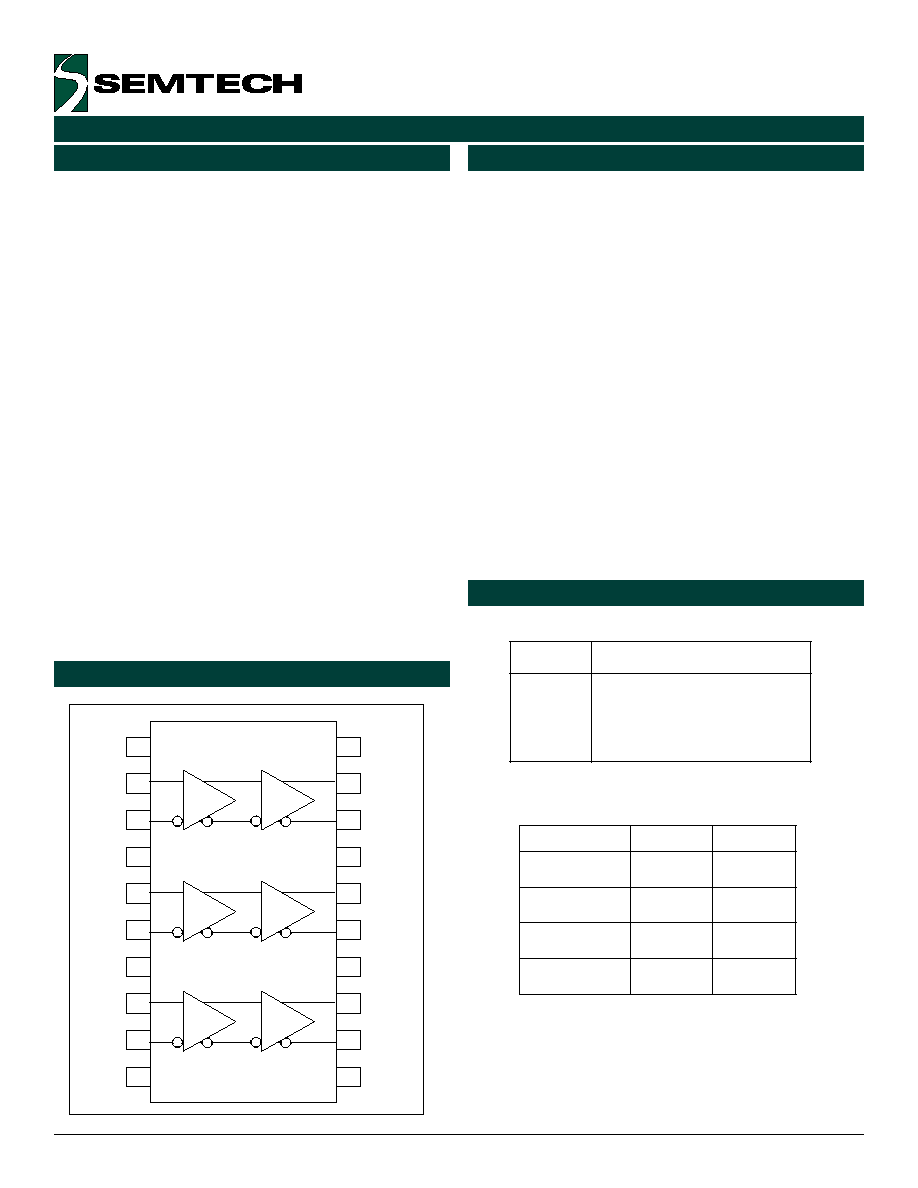
.unctional Block Diagram
Pin Names
The SK10/100EL90W is a triple ECL to PECL/LVPECL and
LVECL to PECL/LVPECL translator. It is fully compatible
with MC100EL90 and MC100LVEL90. The SK10/
100EL90W provides a V
BB
output for single-ended use
or DC bias for AC coupling to the device. V
BB
is an output
pin and should be used as a bias for the EL90W as its
current source/sink capability is limited. Whenever used,
the V
BB
output pin should be bypassed to V
CC
via a 0.01
µF capacitor.
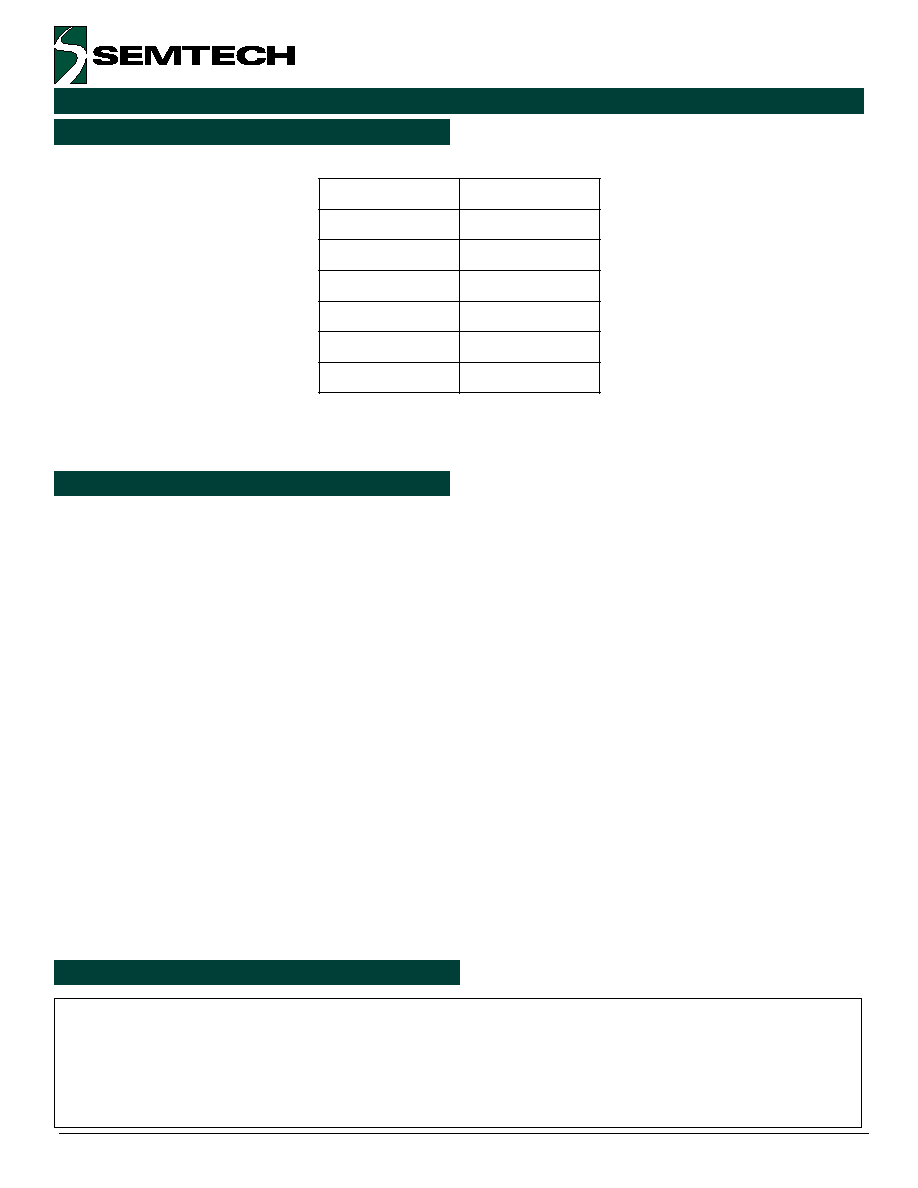
To accomplish levels of translation, the EL90W requires
three power rails, V
CC
, V
EE
and GND. Please refer to the
Function Table below for more details. V
CC
supply should
be connected to the positive supply, and V
EE
should be
connected to the negative supply.
The GND pins are connected to the system ground plane.
Both V
CC
and V
EE
pins should be bypassed to ground via
a 0.01 µF capacitor. Under open input conditions, the D*
input will be biased at V
EE
/2, and the D input will be pulled
to V
EE
. This condition will force the Q output to low,
ensuring stability.
·
Extended Supply Voltage Range (V
EE
= 5.5V to
3.0V and V
CC
= 3.0V to 5.5V)
·
High Bandwidth Output Transition
·
500 ps Propagation Delay
·
V
BB
Output
·
Internal Input Pulldown Resistors
·
New Differential Input Common Mode Range
·
Fully Compatible with MC100EL90 and
MC100LVEL90
·
ESD Protection of >4000V
·
Industrial Temperature Range: 40
o
C to +85
o
C
·
Available in 20-lead SOIC Package
Function Table
n
i
P
n
o
i
t
c
n
u
F
*
n
D
,
n
D
s
t
u
p
n
I
L
C
E
V
L
/
L
C
E
l
a
i
t
n
e
r
e
f
f
i
D
*
n
Q
,
n
Q
s
t
u
p
t
u
O
L
C
E
P
V
L
/
L
C
E
P
l
a
i
t
n
e
r
e
f
f
i
D
V
B
B
t
u
p
t
u
O
e
g
a
t
l
o
V
e
c
n
e
r
e
f
e
R
L
C
E
V
L
/
L
C
E
n
o
i
t
c
n
u
F
E
E
V
C
C
V
L
C
E
P
-
o
t
-
L
C
E
V
L
V
3
.
3
-
V
0
.
5
+
L
C
E
P
V
L
-
o
t
-
L
C
E
V
L
V
3
.
3
-
V
3
.
3
+
L
C
E
P
-
o
t
-
L
C
E
V
0
.
5
-
V
0
.
5
+
L
C
P
E
V
L
-
o
t
-
L
C
E
V
0
.
5
-
V
3
.
3
+
VCC
D0
D1
D1*
VBB
D2
D2*
VEE
D0*
VBB
VCC
Q0
Q1
Q1*
GND
Q2
Q2*
VCC
Q0*
GND
1
2
3
4
5
6
7
8
9
10
20
19
18
17
16
15
14
13
12
11
ECL
PECL
ECL
PECL
ECL
PECL
2
www.semtech.com
HIGH-PER.ORMANCE PRODUCTS
SK10/100EL90W
Revision 1/May 09, 2002
PRELIMINARY
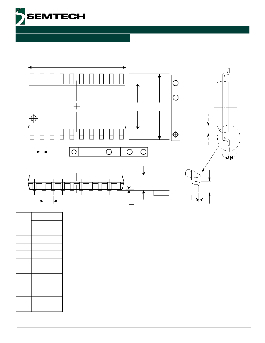
Package Information
PIN Descriptions
20 Pin SOIC Package
e
A
A1
T
18X
SEATING
PLANE
C
L
h
x 45
°
B
D
H
E
10X
20X
20
11
0.010 (0.25) M
T
A
S
B
S
0.010 (0.25)
M
BM
NOTES:
1.
Dimensions and tolerances per ASME Y14.5M,
1994.
2.
Controlling dimension: millimeters.
3.
Dimensions D and E do not include mold protrusion.
4.
Maximum mold protrusion 0.15 per side.
5.
Dimension B does not include Dambar protrusion.
Allowable Dambar protrusion shall be 0.13 total in
excess of B dimension at maximum material
condition.
s
r
e
t
e
m
i
l
l
i
M
M
I
D
N
I
M
X
A
M
A
5
3
.
2
5
6
.
2
1
A
0
1
.
0
5
2
.
0
B
5
3
.
0
9
4
.
0
C
3
2
.
0
2
3
.
0
D
5
6
.
2
1
5
9
.
2
1
E
0
4
.
7
0
6
.
7
e
C
S
B
7
2
.
1
H
5
0
.
0
1
5
5
.
0
1
h
5
2
.
0
5
7
.
0
L
0
5
.
0
0
9
.
0
0
o
7
o
3
www.semtech.com
HIGH-PER.ORMANCE PRODUCTS
SK10/100EL90W
PRELIMINARY
Revision 1/May 09, 2002
0
4
-
=
A
T
o
C
0
=
A
T
o
C
5
2
+
=
A
T
o
C
5
8
+
=
A
T
o
C
l
o
b
m
y
S
c
i
t
s
i
r
e
t
c
a
r
a
h
C
n
i
M
x
a
M
n
i
M
x
a
M
n
i
M
x
a
M
n
i
M
x
a
M
t
i
n
U
V
H
I
e
g
a
t
l
o
V
H
G
I
H
t
u
p
n
I
L
E
0
1
L
E
0
0
1
0
3
2
1
-
5
6
1
1
-
0
9
8
-
0
8
8
-
0
7
1
1
-
5
6
1
1
-
0
4
8
-
0
8
8
-
0
3
1
1
-
5
6
1
1
-
0
1
8
-
0
8
8
-
0
6
0
1
-
5
6
1
1
-
0
2
7
-
0
8
8
-
V
m
V
m
V
L
I
e
g
a
t
l
o
V
W
O
L
t
u
p
n
I
L
E
0
1
L
E
0
0
1
0
5
9
1
-
0
1
8
1
-
0
0
5
1
-
5
7
4
1
-
0
5
9
1
-
0
1
8
1
-
0
8
4
1
-
5
7
4
1
-
0
5
9
1
-
0
1
8
1
-
0
8
4
1
-
5
7
4
1
-
0
5
9
1
-
0
1
8
1
-
5
4
4
1
-
5
7
4
1
-
V
m
V
m
V
B
B
e
g
a
t
l
o
V
e
c
n
e
r
e
f
e
R
t
u
p
n
I
L
E
0
1
L
E
0
0
1
0
3
4
1
-
0
8
3
1
-
0
0
3
1
-
0
6
2
1
-
0
8
3
1
-
0
8
3
1
-
0
7
2
1
-
0
6
2
1
-
0
5
3
1
-
0
8
3
1
-
0
5
2
1
-
0
6
2
1
-
0
1
3
1
-
0
8
3
1
-
0
9
1
1
-
0
6
2
1
-
V
m
V
m
I
N
I
)
f
f
i
D
(
t
n
e
r
r
u
C
t
u
p
n
I
0
5
1
-
0
5
1
0
5
1
-
0
5
1
0
5
1
-
0
5
1
0
5
1
-
0
5
1
A
µ
I
E
E
t
n
e
r
r
u
C
y
l
p
p
u
S
r
e
w
o
P
2
6
2
6
2
6
2
6
A
m
0
4
-
=
A
T
o
C
0
=
A
T
o
C
5
2
+
=
A
T
o
C
5
8
+
=
A
T
o
C
l
o
b
m
y
S
c
i
t
s
i
r
e
t
c
a
r
a
h
C
n
i
M
x
a
M
n
i
M
x
a
M
n
i
M
x
a
M
n
i
M
x
a
M
t
i
n
U
n
o
i
t
i
d
n
o
C
V
H
O
e
g
a
t
l
o
V
H
G
I
H
t
u
p
t
u
O
L
E
0
1
2
9
.
3
2
2
.
2
1
1
.
4
1
4
.
2
8
9
.
3
8
2
.
2
6
1
.
4
6
4
.
2
2
0
.
4
2
3
.
2
9
1
.
4
9
4
.
2
9
0
.
4
9
3
.
2
8
2
.
4
8
5
.
2
V
V
V
C
C
V
5
=
V
C
C
V
3
.
3
=
V
H
O
e
g
a
t
l
o
V
H
G
I
H
t
u
p
t
u
O
L
E
0
0
1
5
1
9
.
3
5
1
2
.
2
2
1
.
4
2
4
.
2
5
7
9
.
3
5
7
2
.
2
2
1
.
4
2
4
.
2
5
7
9
.
3
5
7
2
.
2
2
1
.
4
2
4
.
2
5
7
9
.
3
5
7
2
.
2
2
1
.
4
2
4
.
2
V
V
V
C
C
V
5
=
V
C
C
V
3
.
3
=
V
L
O
e
g
a
t
l
o
V
W
O
L
t
u
p
t
u
O
L
E
0
1
5
0
.
3
5
3
.
1
5
3
.
3
5
6
.
1
5
0
.
3
5
3
.
1
7
3
.
3
7
6
.
1
5
0
.
3
5
3
.
1
7
3
.
3
7
6
.
1
5
0
.
3
5
3
.
1
5
0
4
.
3
5
0
7
.
1
V
V
V
C
C
V
5
=
V
C
C
V
3
.
3
=
V
L
O
e
g
a
t
l
o
V
W
O
L
t
u
p
t
u
O
L
E
0
0
1
7
1
.
3
7
4
.
1
5
4
4
.
3
5
4
7
.
1
9
1
.
3
9
4
.
1
8
3
.
3
8
6
.
1
9
1
.
3
9
4
.
1
8
3
.
3
8
6
.
1
9
1
.
3
9
4
.
1
8
3
.
3
8
6
.
1
V
V
V
C
C
V
5
=
V
C
C
V
3
.
3
=
I
D
N
G
t
n
e
r
r
u
C
y
l
p
p
u
S
r
e
w
o
P
L
E
0
1
L
E
0
0
1
7
1
7
1
2
3
5
3
7
1
7
1
2
3
5
3
7
1
7
1
2
3
5
3
7
1
7
1
2
3
5
3
A
m
A
m
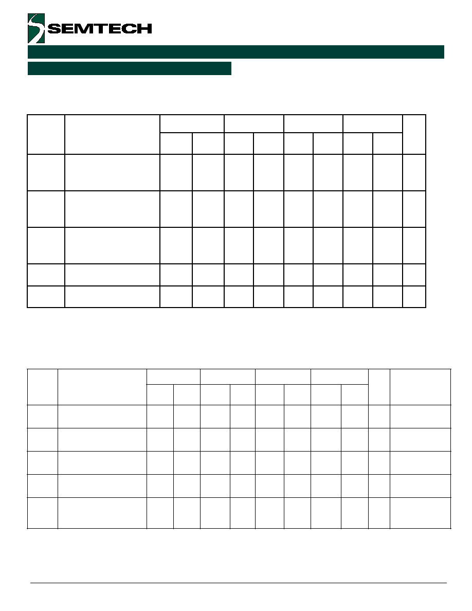
SK10/100EL90W PECL/LVPECL Output DC Electrical Characteristics (Notes 1, 2)
(V
EE
= 5.5V to 3.0V; V
CC
= +3.0V to +5.5V; V
OUT
loaded 50
to V
CC
2.0V)
SK10/100EL90W ECL/LVECL Input DC Electrical Characteristics (Notes 1, 2, 6)
(V
EE
= 5.5V to 3.0V; V
CC
= +3.0V to +5.5V ; V
OUT
loaded 50
to V
CC
2.0V)
DC Characteristics
4
www.semtech.com
HIGH-PER.ORMANCE PRODUCTS
SK10/100EL90W
Revision 1/May 09, 2002
PRELIMINARY
0
4
-
=
A
T
o
C
0
=
A
T
o
C
5
2
+
=
A
T
o
C
5
8
+
=
A
T
o
C
l
o
b
m
y
S
c
i
t
s
i
r
e
t
c
a
r
a
h
C
n
i
M
x
a
M
n
i
M
x
a
M
n
i
M
x
a
M
n
i
M
x
a
M
t
i
n
U
t
w
e
k
s
w
e
k
S
t
u
p
t
u
O
o
t
t
u
p
t
u
O
0
0
1
0
0
1
0
0
1
0
0
1
s
p
t
L
H
P
t
H
L
P
y
a
l
e
D
n
o
i
t
a
g
a
p
o
r
P
)
f
f
i
D
(
3
0
2
4
0
3
5
5
3
4
0
5
5
0
4
4
0
6
5
0
6
4
5
8
5
s
p
t
H
L
P
t
H
P
y
a
l
e
D
n
o
i
t
a
g
a
p
o
r
P
)
E
S
(
3
5
3
4
5
4
5
0
5
4
5
6
5
0
6
4
0
8
5
0
7
4
5
0
6
s
p
t
r
t
,
f
s
e
m
i
T
l
l
a
F
/
e
s
i
R
t
u
p
t
u
O
)
%
0
8
o
t
%
0
2
(
5
7
2
0
7
4
5
7
2
0
7
4
5
7
2
0
7
4
5
7
2
0
7
4
s
p
V
R
M
C
e
g
n
a
R
e
d
o
M
n
o
m
m
o
C
5
+
E
E
V
2
.
1
D
N
G
+
E
E
V
2
.
1
D
N
G
+
E
E
V
2
.
1
D
N
G
+
E
E
V
2
.
1
D
N
G
V
V
P
P
g
n
i
w
S
t
u
p
n
I
m
u
m
i
n
i
M
4
0
5
1
0
0
0
1
0
5
1
0
0
0
1
0
5
1
0
0
0
1
0
5
1
0
0
0
1
V
m
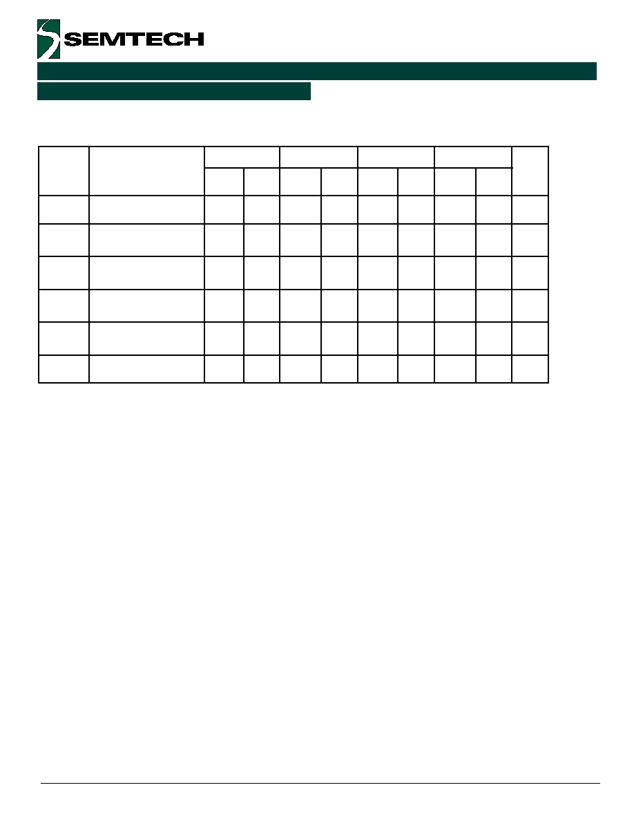
AC Characteristics
SK10/100EL90W AC Electrical Characteristics
Notes:
1.
10EL circuits are designed to meet the DC specifications shown in the table after thermal equilibrium has
been established. The circuit is in a test socket or mounted on a printed circuit board and transverse
airflow greater than 500 lfpm is maintained. Outputs are terminated through a 50
resistor to
VCC2.0V.
2.
100K circuits are designed to meet the DC specification shown in the table where transverse
airflow greater than 500 lfpm is maintained.
3.
Duty cycle skew is the difference between T
PLH
and T
PHL
propagation delay through a device.
4.
Minimum input swing for which parameters guaranteed.
5.
CMR range is referenced to the most positive side of the differential input signal. Normal operation is
obtained if the high level falls within the specified range and the peak-to-peak voltage lies between
VPP
(min)
and 1V. The lower end of the CMR range varies 1:1 with VEE and is equal to VEE + 1.2V.
6.
For standard ECL DC specifications, refer to the ECL Logic Family Standard DC Specifications Data
Sheet.
7.
For part ordering description, see HPP Part Ordering Information Data Sheet.
(V
EE
= 5.5V to 3.0V; V
CC
= +3.0V to +5.5V ; V
OUT
loaded 50
to V
CC
2.0V)
5
www.semtech.com
HIGH-PER.ORMANCE PRODUCTS
SK10/100EL90W
PRELIMINARY
Revision 1/May 09, 2002
Ordering Information
e
d
o
C
g
n
i
r
e
d
r
O
D
I
e
g
a
k
c
a
P
D
W
0
9
L
E
0
1
K
S
C
I
O
S
-
0
2
T
D
W
0
9
L
E
0
1
K
S
C
I
O
S
-
0
2
D
W
0
9
L
E
0
0
1
K
S
C
I
O
S
-
0
2
T
D
W
0
9
L
E
0
0
1
K
S
C
I
O
S
-
0
2
U
W
0
9
L
E
0
1
K
S
e
i
D
U
W
0
9
L
E
0
0
1
K
S
e
i
D
Division Headquarters
10021 Willow Creek Road
San Diego, CA 92131
Phone: (858) 695-1808
FAX: (858) 695-2633
Marketing Group
1111 Comstock Street
Santa Clara, CA 95054
Phone: (408) 566-8776
FAX: (408) 566-8759
Semtech Corporation
High-Performance Products Division
Contact Information
AN1002 - Interfacing Between ECL / LVECL / PECL / LVPECL - to - TTL / LVTTL / CMOS / LVCMOS
AN1003 - Termination Techniques for ECL / LVECL / PECL / LVPECL Devices
AN1004 - Interfacing Between LVDS and ECL / LVECL / PECL / LVPECL
AN1005 - Using ECL / LVECL Devices as PECL / LVPECL
AN1006 - Designing with 10K and 100K ECL / PECL Devices
Application Notes