
HIGH-PERFORMANCE PRODUCTS
1
www.semtech.com
Revision 3/December 17, 2001
SK100EL16Y
High Gain Differential Receiver
with Variable Output Swing
Description
Features
Functional Block Diagram
The SK100EL16Y is a high gain differential receiver with
variable output swing. Its VCTRL input controls the
amplitude of the Q
HG
and Q
HG
* outputs. The operating
range of the EL16Y control input, VCTRL, is from VBB
(large swing) to VCC (min swing), see Figure 2. Simple
control of the output swing can be obtained by a variable
resistor between the VBB and VCC pins, with wiper
driving CTRL. Typical application circuit and results
are described in Figures 1a, 1b, and 2.
The SK100EL16Y provides a VBB output for either single-
ended use or as a DC bias for AC coupling to the device.
The VBB pin should be used only as a bias for the EL16Y
as its current sink/source capability is limited. Whenever
used, the VBB pin should be bypassed to VCC via a 0.01
µF capacitor.
The VCTRL pin should be bypassed to VCC via a 0.01
µF capacitor when the pin is used.
·
Extended Supply Voltage Range: (VEE = 5.5V to
3.0V, VCC = 0V) or (VCC = +3.0V to +5.5V, VEE =
0V)
·
High Bandwidth Output Transitions
·
400 ps Propagation Delay (typical)
·
VBB Output
·
New Differential Input Common Mode Range
·
ESD Protection of >4000V
·
Specified Over Industrial Temperature Range:
40
o
C to 85
o
C
·
Available in Both 8 Pin SOIC (150 mil) and MSOP
(3mm x 3mm) Packages
·
Flammability Rate: UL-94 code V-0.
·
Moisture Sensitivity: Level 1.
PIN Description
n
i
P
n
o
i
t
c
n
u
F
*
D
,
D
s
t
u
p
n
I
a
t
a
D
l
a
i
t
n
e
r
e
f
f
i
D
Q
G
H
Q
,
G
H
*
s
t
u
p
t
u
O
a
t
a
D
l
a
i
t
n
e
r
e
f
f
i
D
B
B
V
t
u
p
t
u
O
e
g
a
t
l
o
V
f
e
R
B
B
V
L
R
T
C
V
l
o
r
t
n
o
C
g
n
i
w
S
t
u
p
t
u
O
1
2
3
4
8
7
6
5
VCTRL
VBB
D
D*
VCC
VEE
QHG
QHG*
2
www.semtech.com
HIGH-PERFORMANCE PRODUCTS
SK100EL16Y
Revision 3/December 17, 2001
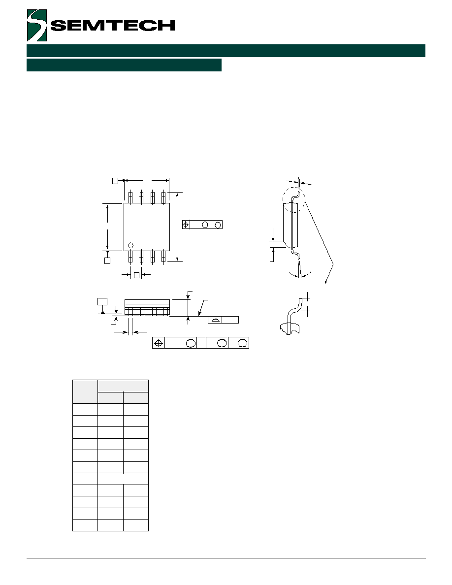
Package Information
NOTES:
1.
Dimensions are in millimeters.
2.
Dimensions D and E do no include mold protrusion.
3.
Maximum mold protrusion 0.15 per side.
4.
Dimension B does not include Dambar protrusion.
Allowable Dambar protrusion shall be 0.127 total
in excess of the B dimension at maximum material
condition.
S
R
E
T
E
M
I
L
L
I
M
M
I
D
N
I
M
X
A
M
A
5
3
.
1
5
7
.
1
1
A
0
1
.
0
5
2
.
0
B
3
3
.
0
1
5
.
0
C
9
1
.
0
5
2
.
0
D
0
8
.
4
0
0
.
5
E
0
8
.
3
0
0
.
4
e
7
2
.
1
C
S
B
H
0
8
.
5
0
2
.
6
h
5
2
.
0
0
5
.
0
L
0
4
.
0
7
2
.
1
q
0
o
8
o
END VIEW
h x 45
o
C
q
L
TOP VIEW
8
5
1
4
D
E
H
e
B
A
0.25 M B M
B
C
A1
A
0.25 M C B S A S
0.10
Seating
Plane
8 Pin SOIC Package

3
www.semtech.com
HIGH-PERFORMANCE PRODUCTS
SK100EL16Y
Revision 3/December 17, 2001
Package Information (continued)
NOTES:
1.
Dimensions are in mm.
2.
Controlling dimension: mm
3.
Dimension does not include mold flash or
protrusions, either of which shall not
exceed 0.20.
8 Pin MSOP Package
M
I
D
N
I
M
X
A
M
A
4
9
.
0
1
.
1
B
1
2
.
0
5
4
.
0
C
3
1
.
0
2
2
.
0
D
0
9
.
2
0
1
.
3
E
0
9
.
2
0
1
.
3
e
5
6
.
0
C
S
B
H
7
.
4
1
.
5
L
4
.
0
7
.
0
q
0
o
6
o
Millimeters
5
4
8
1
TOP VIEW
BOTTOM VIEW
END VIEW
DETAIL A
See Detail A
H
E
B
e
D
A
C
L
q

4
www.semtech.com
HIGH-PERFORMANCE PRODUCTS
SK100EL16Y
Revision 3/December 17, 2001
DC Characteristics
0
4
-
=
A
T
o
C
0
=
A
T
o
C
5
2
+
=
A
T
o
C
5
8
+
=
A
T
o
C
l
o
b
m
y
S
c
i
t
s
i
r
e
t
c
a
r
a
h
C
n
i
M
p
y
T
x
a
M
n
i
M
p
y
T
x
a
M
n
i
M
p
y
T
x
a
M
n
i
M
p
y
T
x
a
M
t
i
n
U
n
o
i
t
i
d
n
o
C
f
x
a
m
y
c
n
e
u
q
e
r
F
e
l
g
g
o
T
m
u
m
i
x
a
M
3
5
.
2
5
.
2
5
.
2
5
.
2
z
H
G
t
H
L
P
t
L
H
P
t
u
p
t
u
O
o
t
y
a
l
e
D
n
o
i
t
a
g
a
p
o
r
P
)
F
F
I
D
(
0
5
2
0
0
3
0
5
3
0
5
2
0
0
3
0
5
3
0
5
2
5
0
3
0
6
3
0
5
2
5
1
3
0
8
3
s
p
A
V
n
i
a
G
l
a
n
g
i
S
ll
a
m
S
4
3
4
3
4
3
4
3
4
B
d
t
w
e
k
s
w
e
k
S
e
l
c
y
C
y
t
u
D
2
)
F
F
I
D
(
5
0
2
5
0
2
5
0
2
5
0
2
s
p
t
r
t
,
f
Q
s
e
m
i
T
ll
a
F
/
e
s
i
R
t
u
p
t
u
O
G
H
)
%
0
8
o
t
%
0
2
(
0
8
0
2
1
0
4
1
0
8
0
2
1
0
4
1
0
9
0
2
1
0
5
1
0
9
5
3
1
0
8
1
s
p
V
R
M
C
e
g
n
a
R
e
d
o
M
n
o
m
m
o
C
6
V
E
E
5
.
1
+
C
C
V
V
E
E
5
.
1
+
C
C
V
V
E
E
5
.
1
+
C
C
V
V
E
E
5
.
1
+
C
C
V
V
V
P
P
g
n
i
w
S
t
u
p
n
I
l
a
i
t
n
e
r
e
f
f
i
D
5
0
5
1
0
0
0
1
0
5
1
0
0
0
1
0
5
1
0
0
0
1
0
5
1
0
0
0
1
V
m
O
V
P
-
P
e
g
a
t
l
o
V
t
u
p
t
u
O
7
0
0
2
0
0
2
0
0
2
0
0
2
V
m
V
L
R
T
C
V
=
C
C
0
4
=
A
T
o
C
0
=
A
T
o
5
8
+
o
t
C
o
C
l
o
b
m
y
S
c
i
t
s
i
r
e
t
c
a
r
a
h
C
n
i
M
x
a
M
n
i
M
x
a
M
t
i
n
U
n
o
i
t
i
d
n
o
C
V
H
O
e
g
a
t
l
o
V
H
G
I
H
t
u
p
t
u
O
8
5
8
0
1
0
8
8
5
2
0
1
0
8
8
V
m
V
N
I
V
=
x
a
m
H
I
V
r
o
n
i
m
L
I
V
L
O
e
g
a
t
l
o
V
W
O
L
t
u
p
t
u
O
8
0
5
9
1
5
5
5
1
0
5
9
1
0
2
6
1
V
m
V
N
I
V
=
x
a
m
H
I
V
r
o
n
i
m
L
I
V
H
I
e
g
a
t
l
o
V
H
G
I
H
t
u
p
n
I
5
6
1
1
0
8
8
5
6
1
1
0
8
8
V
m
s
t
u
p
n
i
l
l
a
r
o
f
l
a
n
g
i
s
H
G
I
H
d
e
e
t
n
a
r
a
u
G
V
L
I
e
g
a
t
l
o
V
W
O
L
t
u
p
n
I
0
1
8
1
5
7
4
1
0
1
8
1
5
7
4
1
V
m
s
t
u
p
n
i
l
l
a
r
o
f
l
a
n
g
i
s
W
O
L
d
e
e
t
n
a
r
a
u
G
V
B
B
e
g
a
t
l
o
V
t
u
p
t
u
O
e
c
n
e
r
e
f
e
R
0
3
4
1
-
0
6
2
1
-
0
3
4
1
-
0
6
2
1
-
V
m
I
E
E
t
n
e
r
r
u
C
y
l
p
p
u
S
r
e
w
o
P
5
4
5
4
A
m
I
N
I
:
t
n
e
r
r
u
C
t
u
p
n
I
)
f
f
i
D
(
*
D
,
D
)
E
S
(
L
R
T
C
V
0
5
1
0
5
1
0
5
1
0
5
1
A
µ
A
µ
(V
EE
= 3.0V to 5.5V; V
CC
= 0V; V
OUT
loaded 50
W to V
CC
2.0V)
SK100EL16Y DC Electrical Characteristics (Note 1)
SK100EL16Y AC Electrical Characteristics
(V
CC
V
EE
= 3.0V to 5.5V; V
OUT
loaded 50
W to V
CC
2.0V)
AC Characteristics

5
www.semtech.com
HIGH-PERFORMANCE PRODUCTS
SK100EL16Y
Revision 3/December 17, 2001
Notes:
1.
100K circuits are designed to meet the DC specification shown in the table where transverse airflow
greater than 500 lfpm is maintained.
2.
Duty cycle skew is the difference between T
PLH
and T
PHL
propagation delay through a device.
3.
F
max
guaranteed for functionality only. See Figure 3 for typical output swing. VO
P-P
levels are guaranteed
at DC only.
4.
The device has a DC gain of ~140.
5.
Minimum input swing for which parameters are guaranteed.
6.
CMR range is referenced to the most positive side of the differential input signal. Normal operation is
obtained if the high level falls within the specified range and the peak-to-peak voltage lies between
VPP
(min)
and 1V. The lower end of the CMR range varies 1:1 with VEE and is equal to VEE + 1.5V.
7.
VO
P-P
is obtained as follows: Voltages of Q
HG
and Q
HG
* outputs with respect to VCC are measured. The
absolute difference between a high and a low state is equal to VO
P-P
.
8.
The VOH and VOL limits apply when the V
CTRL
pin is left open. Otherwise, see figure 2.
9.
For part ordering description, see HPP Part Ordering Information Data Sheet.

6
www.semtech.com
HIGH-PERFORMANCE PRODUCTS
SK100EL16Y
Revision 3/December 17, 2001
Figure 2. Typical Voltage Output Swing at 25
o
C
100
75
50
25
0
V
EE
V
CC
1.32
V
CC
0.8
V
CC
0.4
V
CC
V
CTRL
= Open
Voltage Control (V)
V
oltage S
w
ing (% pk-pk diff
er
ential)
Figure 1B
Implementation of Voltage Source
Figure 1A
Note: R1 = R2 150
W for VCC = 3.3V
R1 = R2 330
W for VCC = 5.0V
Note: R1 = R2 150
W for VCC = 3.3V
R1 = R2 330
W for VCC = 5.0V
1
2
3
4
8
7
6
5
VCTRL
VBB
VCC
D
D*
VCC
VSWING
(pk-pk)
GND
QHG
QHG*
R1
R2
10K
1
2
3
4
8
7
6
5
VCTRL
VBB
VCC
D
D*
VCC
VSWING
(pk-pk)
GND
QHG
QHG*
+
R1
R2
AC Characteristics (continued)

7
www.semtech.com
HIGH-PERFORMANCE PRODUCTS
SK100EL16Y
Revision 3/December 17, 2001
Figure 3. Typical Output VO
P-P
vs. Frequency
AC Characteristics (continued)
Typical Output Voltage, VOP-P vs. Frequency
0
100
200
300
400
500
600
700
800
900
0.5
1.5
2.5
3.5
Frequency (GHz)
VPP A
m
p
l
i
t
u
d
e
(mV)
VPP_IN=800 mV
VPP_IN=20mV
e
d
o
C
g
n
i
r
e
d
r
O
D
I
e
g
a
k
c
a
P
e
g
n
a
R
e
r
u
t
a
r
e
p
m
e
T
D
Y
6
1
L
E
0
0
1
K
S
C
I
O
S
-
8
l
a
i
r
t
s
u
d
n
I
T
D
Y
6
1
L
E
0
0
1
K
S
C
I
O
S
-
8
l
a
i
r
t
s
u
d
n
I
S
M
Y
6
1
L
E
0
0
1
K
S
P
O
S
M
-
8
l
a
i
r
t
s
u
d
n
I
T
S
M
Y
6
1
L
E
0
0
1
K
S
P
O
S
M
-
8
l
a
i
r
t
s
u
d
n
I
U
Y
6
1
L
E
0
0
1
K
S
e
i
D
Ordering Information

8
www.semtech.com
HIGH-PERFORMANCE PRODUCTS
SK100EL16Y
Revision 3/December 17, 2001
Division Headquarters
10021 Willow Creek Road
San Diego, CA 92131
Phone: (858) 695-1808
FAX: (858) 695-2633
Marketing Group
1111 Comstock Street
Santa Clara, CA 95054
Phone: (408) 566-8776
FAX: (408) 727-8994
Semtech Corporation
High-Performance Products Division
Contact Information
Marking Information
Function / Voltage &
Device Operation
Function Code / Part Number
H = 10
K = 100
YY: Last two digits of the Year
WW: Working Week
E
L
W
W
Y
Y
8 PIN SOIC PACKAGE
Assembly
Lot Number
Function / Voltage Option
Function Code / Part Number
Assembly Lot Number
Assembly Date Code
SK10EL/ELT = H
SK100EL/ELT = K
8/10 PIN MSOP PACKAGES
AN1002 - Interfacing Between ECL / LVECL / PECL / LVPECL - to - TTL / LVTTL / CMOS / LVCMOS
AN1003 - Termination Techniques for ECL / LVECL / PECL / LVPECL Devices
AN1005 - Using ECL / LVECL Devices as PECL / LVPECL
Application Notes
AN1006 - Designing with 10K and 100K ECL / PECL Devices