20MHZ ~ 100MHZ FSPLL
PLL2126X (PRELIMINARY)
1
GENERAL DESCRIPTION
The pll2126x is a Phase Locked Loop (PLL) frequency synthesizer. The PLL provide frequency multiplication
capabilities. Its output clock frequency FOUT is related to the input clock frequency FIN by the following
equation:
FOUT = (m
æ
FIN) / (p
æ
2
s
)
where FOUT is the output clock frequency. FIN is the input clock frequency. m, p and s are the values for
programmable dividers. pll2126x consists of a Phase Frequency Detector(PFD), a Charge Pump, an Off-chip
Loop Filter, a Voltage Controlled Oscillator (VCO), a 6-bit Pre-divider, an 8-bit Main-divider and 2-bit Post-scaler
as will be shown in functional block diagram.
FEATURES
-- 0.13um CMOS device technology
-- 1.2V single power supply
-- Output frequency range: 20M ~ 100MHz
-- Jitter:
Ý
200ps at 100MHz
-- Duty ratio: 40% to 60% (All tuned range)
-- Power down mode
-- Off-chip loop filter
-- Frequency is changed by programmable divider
NOTES:
1.
Don't set the P or M as zero, that is 000000 / 00000000
2.
The proper range of P and M: 1
P
62, 1
M
248
3.
The P and M must be selected considering stability of PLL and VCO output frequency range.
4.
Please consult with SEC application engineer to select the proper P, M and S values
.
Ver_1.0 (May. 2003)
No responsibility is assumed by SEC for it s use nor for any infringements of patents or other rights of third parties that may
result from its use. The contents of the datasheet is subject to change without any notice.
20MHZ ~ 100MHZ FSPLL
PLL2126X (PRELIMINARY)
3
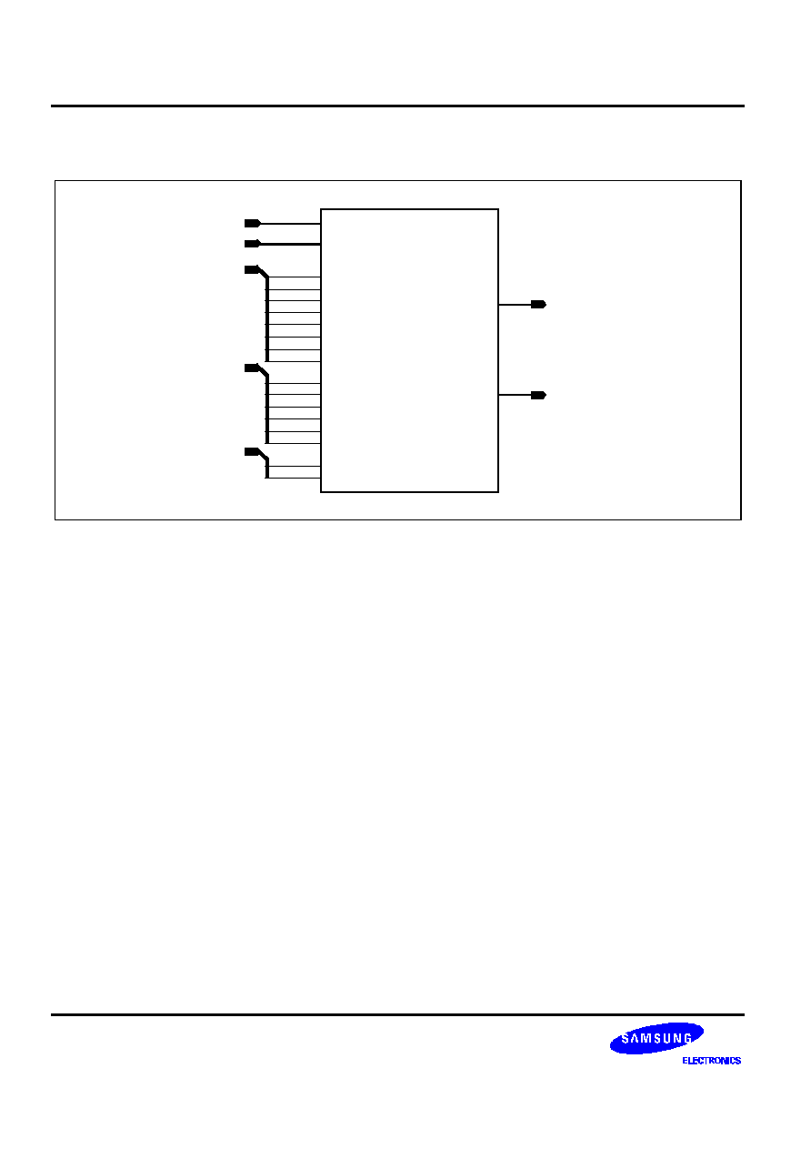
CORE PIN DESCRIPTION
Name
I/O Type
Pin Description
AVDD12D
DP
Digital power supply
AVSS12D
DG
Digital ground
AVDD12A
AP
Analog power supply
AVSS12A
AG
Analog ground
VABB
AB/DB
Analog / Digital bulk bias
FIN
DI
PLL clock input
FOUT
DO
20MHz ~ 100MHz clock output
FILTER
AO
The external loop filter capacitor should be connected between
FILTER and analog ground
PWRDN
DI
Power down.
-If PWRDN is high, power down mode is enabled.
P[5:0]
DI
6-bit programmable pre-divider.
M[7:0]
DI
8-bit programmable main-divider.
S[1:0]
DI
2-bit programmable post-scaler.
I/O Type Abbr.
-- AI: Analog Input
-- DI: Digital Input
-- AO: Analog Output
-- DO: Digital Output
-- AP: Analog Power
-- AG: Analog Ground
-- AB: Analog Sub Bias
-- DP: Digital Power
-- DG: Digital Ground
-- DB: Digital Sub Bias
-- BD: Bi-directional Port

20MHZ ~ 100MHZ FSPLL
PLL2126X (PRELIMINARY)
5
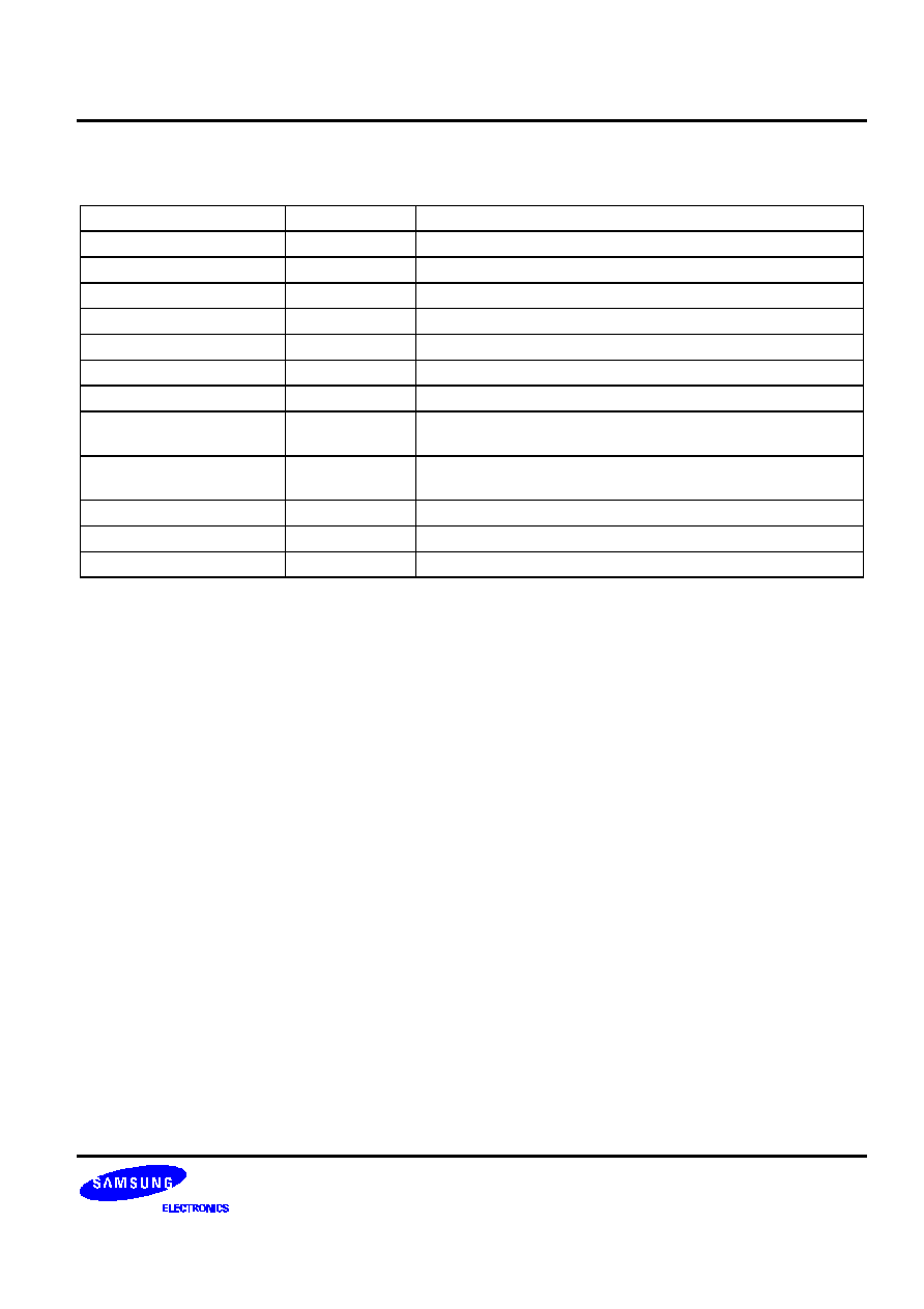
RECOMMENDED OPERATING CONDITIONS
Characteristics
Symbol
Min
Typ
Max
Unit
Supply voltage differential
AVDD12D Ù AVDD12A
Ù0.1
+0.1
V
External loop filter capacitor
LF
700
pF
Operating temperature
Topr
Ù45
85
¯
C
NOTE: It is strongly recommended that all the supply pins (AVDD12D, AVDD12A) be powered to the same supply voltage
to avoid power latch-up.
DC ELECTRICAL CHARACTERISTICS
Characteristics
Symbol
Min
Typ
Max
Unit
Operating voltage
AVDD12D/AVDD12A
1.14
1.20
1.26
V
Dynamic current
I
DD
Ù
Ù
3
mA
Power down current
I
PD
Ù
Ù
TBD
uA
AC ELECTRICAL CHARACTERISTICS
Characteristics
Symbol
Min
Typ
Max
Unit
Input frequency
Fin
10
Ù
40
MHz
Output frequency
Fout
20
Ù
100
MHz
Output clock duty ratio
T
OD
40
50
60
%
Locking time
T
LT
Ù
300
Ù
us
Cycle to cycle jitter
20M ~ 60MH
Z
T
JCC
Ù300
Ù
300
ps
60M ~ 100MH
Z
T
JCC
Ù200
Ù
200
ps