
SEC ASIC
bw0407xa
16Bit 48KHz Sigma-Delta Audio CODEC
ANALOG
1/ 9
GENERAL DESCRIPION
Samsung's BW0407XA is high resolution,
single-chip stereo ADC and DAC that
employs the Sigma-Delta modulation
technique. With a resolution of 16bit,
oversampling of 64X and a 90dB Signal-
to-Noise ratio, BW0407XA is suitable
for applications in consumer digital audio
system, multimedia and digital systems.
TYPICAL APPLICATIONS
- multi-media applications
- consumer digital audio
- digital systems
FEATURES
- 1 chip stereo A/D, D/A converter
- 4-th order Sigma-Delta modulator
- Sigma-Delta Stereo ADC.
* 64X Oversampling
* On-chip Decimation Filter
* On-chip Anti-Aliasing Filter
* 90dB Signal to Noise Ratio.
- Sigma-Delta Stereo DAC.
* 64X Oversampling
* On-chip 4X Interpolation Filter
* On-chip Analog Postfilter
* 90dB Signal to Noise Ratio
- Programmable Gain Amplifier (PGA)
ADC : 0 ~ + 22.5dB (+1.5dB step)
DAC : 0 ~ - 46.5dB (-1.5dB step)
- Mute for Analog Input and Output
- Zero detection mute for DAC
- Analog Single-ended Input and Output.
- Sampling Rate of 48KHz
- Single +3.3V Power Supply
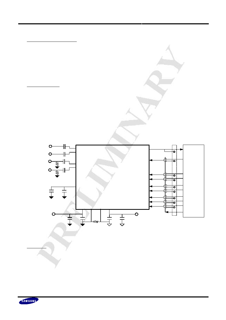
FUNCTIONAL BLOCK DIAGRAM
Record Volume Control
0~+22.5dB & Mute
parallel
interface
&
Control
Logic
AINL
sigma-delta
modulator
(analog)
decimation
filter
sigma-delta
modulator
&
Interpolation
Filter
voltage
reference
AINR
sigma-delta
modulator
(analog)
AOUTL
Analog
postfilter
AOUTR
Analog
postfilter
AUDO[15:0]
AULRCK
AUDI[15:0]
AUSYSCK
VREF
AURST
PWDN[1:0]
Play Volume Control
0~ -46.5dB & Mute
Volume
Control
Register
WREN
ADDR[1:0]
DATA[5:0]
Ver 1.0 (June 1999)
This datasheet is a preliminary version. No responsibility is assumed by SEC for its use nor for any infringements of patents or other
rights of third parties that may result from its use. The content of this datasheet is subject to change without any notice.

SEC ASIC
bw0407xa
16Bit 48KHz Sigma-Delta Audio CODEC
ANALOG
2/ 9
CORE PIN DESCRIPTION
NAME
I/O TYPE
I/O PAD
PIN DESCRIPTION
Analog Pins
AINL
AI
pia_bb_50option
Analog Left Input
AINR
AI
pia_bb_50option
Analog Right Input
AOUTL
AO
poa_bb_50option
Analog Left output
AOUTR
AO
poa_bb_50option
Analog Right output
VREF
AO
poar10_bb
Voltage reference output for bypass filtering
Digital Pins
AUSYSCK
DI
piccbb_bb
Master clock Input (256*Fs)
AULRCK
DI
piccbb_bb
Sampling Frequency clock (Fs)
AUDI[15:0]
DI
piccbb_bb
Digital Parallel input for DAC
AURST
DI
piccbb_bb
Digital reset
PWDN[1:0]
DI
piccbb_bb
Power down control pin
AUDO[15:0]
DO
pot2bb_bb
Digital Parallel output for ADC
WREN
DI
picc_bb
Control Register Write Enable
DATA[5:0]
DI
picc_bb
Control Register Data
ADDR[1:0]
DI
picc_bb
Control Register Address
Power Pins
VDDA
AP
vdd3t_bb
Analog supply
VSSA
AG
vsst_bb
Analog ground
VDDD
DP
vdd3t_bb
Digital supply
VSSD
DG
vsst_bb
Digital ground
I/O Type
Description
AP
Analog Power
AG
Analog Ground
AI
Analog Input
AO
Analog Output
AB
Analog Bidirection
DP
Digital Power
DG
Digital Ground
DI
Digital Input
DO
Digital Output
DB
Digital Bidrection
CORE CONFIGURATION
AUDO[15:0]
AUDI[15:0]
AUSYSCK
AULRCK
AURST
PWDN[1:0]
WREN
ADDR[1:0]
DATA[5:0]
bw0407xa
Power Used:
VDDA VSSA VDDD VSSD
AINL
AINR
AOUTL
AOUTR
VREF
SEC ASIC
bw0407xa
16Bit 48KHz Sigma-Delta Audio CODEC
ANALOG
3/ 9
CORE EVALUATION GUIDE
Power Supply and Grounding
The analog power pins of codec should be derived from the cleanest power source available. The decoupling
capacitors are placed as close as possible to the device. The lowest value capacitor(0.1uF) is placed closest to
the codec. Analog and digital ground connection is done by the ferrite bead only at the one path.
The circuit board layout should have separate analog and digital regions and ground planes. All signal,
especially clocks should be kept away from the VREF pin in order to avoid unwanted coupling into the
modulators and postfilter.
Analog Connections
The analog inputs presented to the BW0407XA are single-ended input voltage through the external coupling
capacitor. The input range is approximately 2.0Vp-p for 0dB gain setting. The analog outputs are also
single-ended through the external coupling capacitor and resistor and the output range are typically 2.0Vp-p for
0dB attenuation setting.
The on-chip voltage reference is output on the VREF pin. A electrolytic capacitor less than 10ĄěF in parallel
with a 0.1ĄěF ceramic capacitor attached to this pin eliminates the effects of high frequency noise. No load
current may be driven from the VREF output pin.
AUDO[15:0]
AUDI[15:0]
AUSYSCK
AULRCK
AURST
PWDN[1:0]
WREN
ADDR[1:0]
DATA[5:0]
bw0407xa
Power Used:
VDDA VSSA VSSD VDDD
AINL
AINR
AOUTL
AOUTR
VREF
0.1uF +
10uF +
0.1uF +
10uF +
+ 0.1uF
+ 10uF
Analog Supply
3.3Volts
Digital Supply
3.3Volts
Ferrite bead
Analog Ground
Digital Ground
Analog Left
Channel Input
Analog Right
Channel Input
Analog Left
Channel Output
Analog Right
Channel Output
100k
100k
+ 1uF
+ 1uF
0.33uF
+
0.33uF
+
Audio
DSP
Mux
Direction
Control
External
Analog Application Circuit & Digital Connection
Digital Pins
Simple examination is shown in the above the figure. By adding the MUX, externally control the codec and
monitor the codec's digital output data and supply the digital input data.
SEC ASIC
bw0407xa
16Bit 48KHz Sigma-Delta Audio CODEC
ANALOG
4/ 9
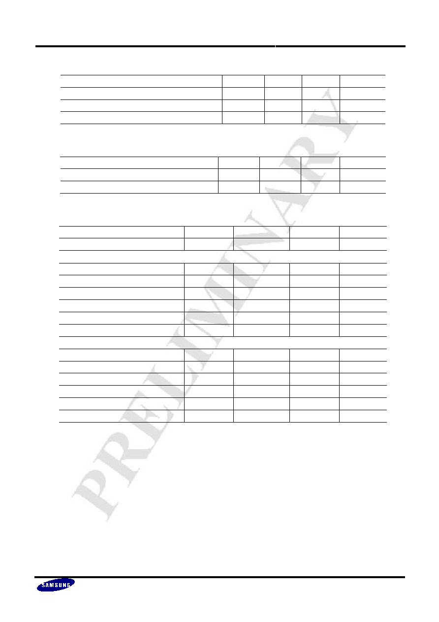
Absolute Maximum Ratings
Charateritics
Min.
Typ.
Max.
Units
Supply Vtg.
-0.3
3.8
V
Digital Input Voltage range
-0.3
3.6
V
Storage Temp.
-65
150
°C
Recommanded Operating Condtions
Charateritics
Min.
Typ.
Max.
Units
Supply Vtg.
3.135
3.3
3.465
V
Operating Temp.
-40
25
85
°C
Digital Filter Characteristics
Characteristics
Min.
Typ.
Max.
Units
Sampling Frequency
4
48
50
KHz
ADC PART
Passband
0
0.4Fs
KHz
Stopband
0.6Fs
ˇÄ
KHz
Transition band
0.4Fs~0.6Fs
KHz
Passband ripple
±0.1
dB
Stopband attenuation
74
dB
Group delay distortion
0
us
DAC PART
Passband
0
0.4Fs
KHz
Stopband
0.6Fs
ˇÄ
KHz
Transition band
0.4Fs~0.6Fs
KHz
Passband ripple
±0.1
dB
Stopband attenuation
74
dB
Group delay distortion
0
us

SEC ASIC
bw0407xa
16Bit 48KHz Sigma-Delta Audio CODEC
ANALOG
5/ 9
Electrical Characteristics
(Measurement Bandwidth is 20Hz ~ 20KHz, Full scale input sine wave 1KHz, Fs=48KHz, VDDA=DVDD=3.3V,
10k
/25§Ü load, Ta=25°C, Record/Play Volume=0dB, Unless otherwise specified)
Characteristics
Min.
Typ.
Max.
Units
Resolution
16
Bits
Sampling rate
4
48
50
KHz
Reference Voltage Output
1.55
V
Record, Play Volume step
1.5
dB
ADC Characteristics
S/N (EIAJ)
85
90
dB
THD
70
77
dB
S/(N+D)
70
77
dB
Dynamic Range
80
85
dB
Interchannel Isolation
70
77
dB
Offset Error
50
mV
Maximum Analog Input Voltage Range
2
Vpp
Analog Input Impedance
10
12
k
DAC Characteristics
S/N (EIAJ)
85
90
dB
THD
70
77
dB
S/(N+D)
70
77
dB
Dynamic Range
80
85
dB
Interchannel Isolation
70
77
dB
Offset Error
50
mV
Maximum Analog Output Voltage Range
2
Vpp
Power Supply
Operating Current
40
mA
Power Dissipation
132
mW
All Power Down Current
1
mA
Power Supply Rejection Ratio
40
dB

SEC ASIC
bw0407xa
16Bit 48KHz Sigma-Delta Audio CODEC
ANALOG
6/ 9
Timing Characteristics
Characteristics
Symbol
Min
Typ
Max
Unit
AUSYSCK Frequency
Fsysck
1.024
12.288
12.8
MHz
AULRCK Frequency
Flrck
4
48
50
KHz
AUSYSCK Duty cycle (H:L)
SYDuty
40:60
50:50
60:40
%
AULRCK Duty cycle (H:L)
LRDuty
50:50
50:50
50:50
%
AUSYSCK rising and AULRCK Edge setup
Tslrck
-
24
-
ns
AULRCK and AUDO delay
Tddo
-
2
-
ns
AULRCK and AUDI setup
Tsdi
-
5208
-
ns
AULRCK and AUDI hold
Thdi
-
10
-
ns
WREN minimum pulse width high
Twren
-
156
-
ns
WREN falling and ADDR setup
Tsaddr
-
15
-
ns
WREN falling and ADDR hold
Thaddr
-
15
-
ns
WREN falling and DATA setup
Tsdata
-
15
-
ns
WREN falling and DATA hold
Thdata
-
15
-
ns
1/Fsysck
AUSYSCK
AULRCK
AUDO[15:0]
1/Flrck
Tslrck
Tddo
Tddo
AUDI[15:0]
Tsdi
Thdi
Tsdi
Thdi
Left Parallel 16bits Output
Right Parallel 16bits Output
Left Parallel 16bits Input
Right Parallel 16bits Input
~
~
Twren
Tsaddr
Thaddr
Tsdata
Thdata
ADDR[1:0]
DATA[5:0]
WREN

SEC ASIC
bw0407xa
16Bit 48KHz Sigma-Delta Audio CODEC
ANALOG
7/ 9
CODEC Digital Data Interface Format
The CODEC provides stereo, 16-bit ADC & DAC functions. The digital input and output of the CODEC is through
the parallel input and output ports. All the Codec related clocks are provided externally. The master clock (AUSYSCK)
is 256xFs and the frame sync clock (AULRCK) is Fs. Two clocks must be synchronized to falling edge.
The ADC of CODEC and the other digital block communicates through parallel output. The interface consists of a
frame sync input clock(AULRCK),
parallel data output(AUDO[15:0]). AUDO[15] is MSB and AUDO[0] is LSB. The
ADC output the 16bits left data at the falling edge of AULRCK and the 16bits right data at the rising edge of
AULRCK
The Codec DAC and the other digital block communicates through a parallel input. The interface consists of a frame
sync input clock (AULRCK), a parallel data input(AUDI[15:0]). AUDI[15] is MSB and AUDI[0] is LSB. The DAC
receive the 16bits left data at the low state of AULRCK and the 16bits right data at the high state of AULRCK. On
digital reset or power down, the serial input of the DAC is disabled(all zeros).
AULRCK
Right
AUDO[15:0]
AUDI[15:0]
Left
Right
Left
AUSYSCK
~
~
16bits Parallel Left Output
16bits Parallel Right Output
16bits Parallel Left Input
16bits Parallel Right Input
Volume Control Registers Format
Register Mapping Table
Address
Function
DATA[5:0]
Default
Value
ADDR[1:0]
D5
D4
D3
D2
D1
D0
b'00
Record Volume Left Channel
RMUTE
X
RGL[3]
RGL[2]
RGL[1]
RGL[0]
b'0x0000
b'01
Record Volume Right Channel
RMUTE
X
RGR[3]
RGR[2]
RGR[1]
RGR[0]
b'0x0000
b'10
Play Volume Left Channel
PMUTE
PGL[4]
PGL[3]
PGL[2]
PGL[1]
PGL[0]
b'000000
b'11
Play Volume Right Channel
PMUTE
PGR[4]
PGR[3]
PGR[2]
PGR[1]
PGR[0]
b'000000
Format Diagram
WREN
ADDR[1:0]
DATA[5:0]
~
Address
Data
Address
Data
Each Function
Record Volume Left or Right
(Address 'b00 or 'b01)
Play Volume Left or Right
(Address 'b10 or 'b11)
RMUTE, RG(L/R)[3:0]
FUNCTION
PMUTE, PG(L/R)[4:0]
FUNCTION
0, 0000
0dB (*)
0, 00000
0dB (*)
0, 0001
+1.5dB
0, 00001
-1.5dB
~
~
~
~
0, 1111
+22.5dB
0, 11111
-46.5dB
1, xxxx
-ˇÄ
1, xxxx
-ˇÄ
c.f.) x is don't care, * is default value. After the reset or power on, the register is set to the default value.

SEC ASIC
bw0407xa
16Bit 48KHz Sigma-Delta Audio CODEC
ANALOG
8/ 9
OVER Range
The digital output of the CODEC ADC will produce a positive full scale[7FFF(h)] output for analog input
signal above the maximum input voltage range and a negative full scale [8000(h)] for input below the minimum
input voltage range.
Power Down
There are three power down mode, see the below the table.
PWDN[1:0]
Condition
b'00
All On
b'01
ADC Off, DAC On
b'10
DAC Off, ADC On
b'11
All Off
Reset
The BW0407XA digital block is placed in the reset mode by bringing AURST "H". But Analog block is still
alive. To exit the reset mode, bring AURST to "L", In the reset mode all clock is still operating, the internal
register is in the reset mode. And the volume control register was set to the defaults value.

SEC ASIC
bw0407xa
16Bit 48KHz Sigma-Delta Audio CODEC
ANALOG
9/ 9
FEEDBACK REQUEST
Parameter
Min
Typ
Max
Unit
Remarks
supply voltage
V
Max master clock frequency
Hz
Operating temperature
ˇÉ
Sampling Frequency
Hz
ADC
Dynamic range
dB
Total harmonic distortion
dB
Signal-to-noise ratio
dB
Output format resolution
(Serial/Parallel interface)
Bit
Channel
Mono
Stereo
Power dissipation
mW
Input voltage range
Vpp
ADC offset error
V
ADC group delay
sec
Phase linearity deviation for
passband region
ˇŁ
(Deg)
Peak-to-peak frequency response
ripple for passband region
dB
DAC
Dynamic range
dB
Total harmonic distortion
dB
Signal-to-noise ratio
dB
Input format resolution
(Serial/Parallel interface)
Bit
Channel
Mono
Stereo
Power dissipation
mW
Full scale output voltage range
Vpp
DAC group delay
sec
Phase linearity deviation for
passband region
ˇ¤
(Deg)
Peak-to-peak frequency response
ripple for passband region
dB
It should be quite helpful to our CODEC core development if you specify your system requirements on CODEC in
the following characteristic checking table and fill out the additional questions. We appreciate your interest in our
products. Thank you very much.
- Could you explain external/internal pin configurations as required?
- Specially requested function list :