8-53
8
F
R
O
N
T
-
E
NDS
Product Description
Ordering Information
Typical Applications
Features
Functional Block Diagram
RF Micro Devices, Inc.
7625 Thorndike Road
Greensboro, NC 27409, USA
Tel (336) 664 1233
Fax (336) 664 0454
http://www.rfmd.com
Optimum Technology Matching® Applied
Si BJT
GaAs MESFET
GaAs HBT
Si Bi-CMOS
ü
SiGe HBT
Si CMOS
1
2
3
4
5
6
7
8
16
15
14
13
12
11
10
9
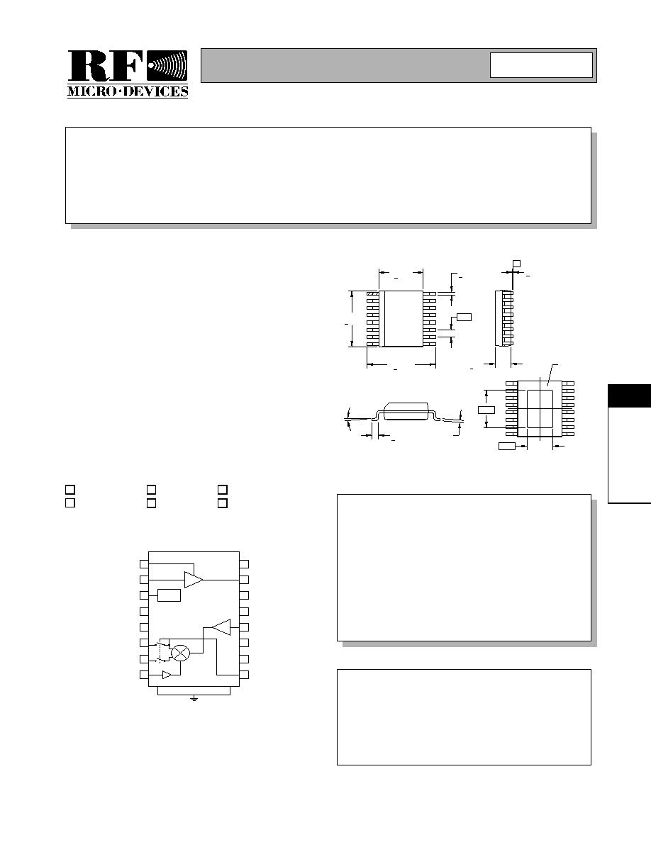
GAIN SEL
LNA IN
PD
VCC1
VCC2
MIX OUT-
MIX OUT+
LO IN
VCC4
LNA OUT
NC
NC
MIXIN
GND3
VCC3
RX EN
LNA
MIXER
RF AMP
Bias
Circuits
BACKSIDE GND
RF2444
HIGH FREQUENCY LNA/MIXER
· WLAN or Wireless Local Loop
· Digital Communication Systems
· Spread-Spectrum Communication Systems
· Part of 2.4GHz Chipset
· Portable Battery-Powered Equipment
· UHF Digital and Analog Receivers
The RF2444 is a monolithic integrated UHF receiver front
end suitable for 2.4GHz ISM band applications. The IC
contains all of the required components to implement the
RF functions of the receiver except for the passive filter-
ing and LO generation. It contains an LNA (low-noise
amplifier), a second RF amplifier and a doubly balanced
mixer. The output of the LNA is made available as an out-
put to permit the insertion of a bandpass filter between
the LNA and the RF/Mixer section. The mixer outputs can
be selectively disabled to allow for the IF filter to be used
in the transmit mode.
· Single 2.7V to 3.6V Power Supply
· 2400MHz to 2500MHz Operation
· Two Gain Settings: 28dB or 12dB
· 4.5dB Cascaded NF, High Gain Mode
· 20mA DC Current Consumption
· Input IP
3
: -23dBm or -8dBm
RF2444
High Frequency LNA/Mixer
RF2444 PCBA-H Fully Assembled Evaluation Board (2.5GHz)
8
Rev A3 010717
NOTES:
1. Shaded lead is pin 1.
2. Lead coplanarity - 0.10 with
respect to datum "A".
3. Lead standoff is specified from the
lowest point on the package underside.
8° MAX
0° MIN
0.60
+ 0.15
0.24
0.20
3.90
+ 0.10
0.25
+ 0.05
0.65
6.00
+ 0.20
4.90
+ 0.20
1.40
+ 0.10
0.05
+ 0.05
Note 3
-A-
Dimensions in mm.
3.302
2.286
EXPOSED DIE
FLAG
Package Style: SSOP-16 EDF Slug
8-54
RF2444
Rev A3 010717
8
F
R
O
N
T
-
E
NDS
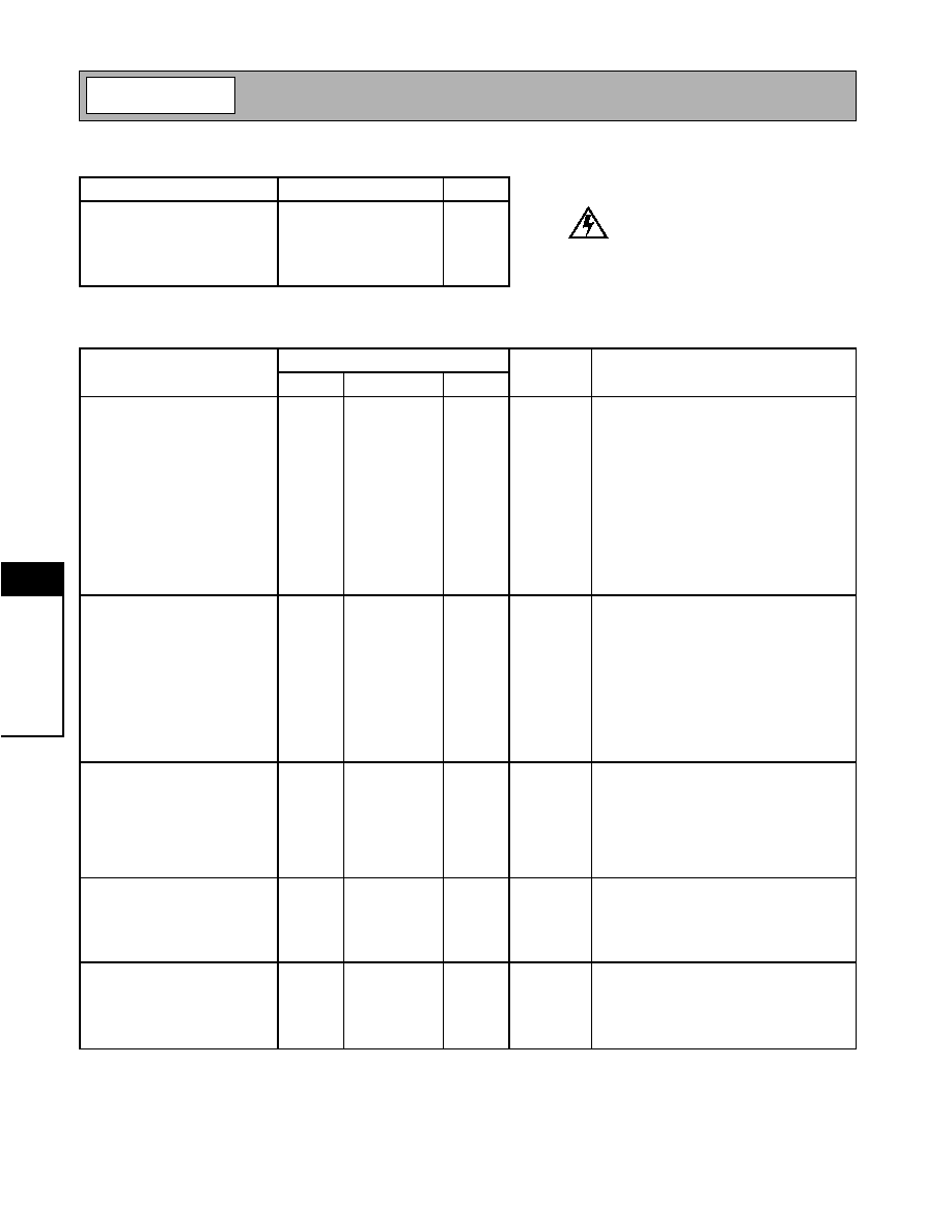
Absolute Maximum Ratings
Parameter
Rating
Unit
Supply Voltage
-0.5 to 3.6
V
DC
Input LO and RF Levels
+6
dBm
Operating Ambient Temperature
-40 to +85
°C
Storage Temperature
-40 to +150
°C
Moisture Sensitivity
JEDEC Level 5 @ 220°C
Parameter
Specification
Unit
Condition
Min.
Typ.
Max.
Overall
T = 25°C, V
CC
= 3.3V, RF = 2400 MHz,
LO= 2120MHz, -1 0 dBm
RF Frequency Range
2400 to 2500
MHz
IF Frequency Range
10
280
500
MHz
Cascade Gain
28
dB
IF = 280MHz, GAIN SEL = 1
12
dB
IF =280MHz, GAIN SEL = 0
Cascade IP3
-23
dBm
Referenced to the input, GAIN SEL = 1
-8
dBm
Referenced to the input, GAIN SEL = 0
Cascade Noise Figure
4.5
dB
Single sideband, GAIN SEL = 1
18
dB
Single sideband, GAIN SEL = 0
Input P1dB
-28
dBm
GAIN SEL = 1
-14
dBm
GAIN SEL = 0
LNA
Noise Figure
2.3
dB
GAIN SEL = 1
7
dB
GAIN SEL = 0
Input VSWR
2:1
No external matching
Input IP3
-3
dBm
GAIN SEL = 1
-3
dBm
GAIN SEL = 0
Gain
10
dB
GAIN SEL = 1
-6
dB
GAIN SEL = 0
Reverse Isolation
22
dB
Output Impedance
50
RF Amp and Mixer
Noise Figure
10
dB
Single sideband
Input Impedance
50
Input IP3
-17
dBm
Conversion Power Gain
18
dB
With Current Combiner (1k
between open
collectors and 250
single ended load)
Output Impedance
4
k
Open Collector
LO Input
LO Level
-15
-10
0
dBm
LO to RF Rejection
42
dB
LO input to LNA input
LO to IF Rejection
15
dB
LO input to IF output
LO Input VSWR
2:1
Power Down Control
Logic Controls "ON"
V
CC
- 0.3
V
Voltage at the input of RX EN, PD
Logic Controls "OFF"
300
mV
and GAIN SEL
Turn on Time
400
1000
nS
From PD Going high.
Turn on Time
100
200
nS
From RX EN Going high. PD = "1"
Caution! ESD sensitive device.
RF Micro Devices believes the furnished information is correct and accurate
at the time of this printing. However, RF Micro Devices reserves the right to
make changes to its products without notice. RF Micro Devices does not
assume responsibility for the use of the described product(s).
Refer to "Handling of PSOP and PSSOP Products"
on page 16-15 for special handling information.

8-55
RF2444
Rev A3 010717
8
F
R
O
N
T
-
E
NDS
Parameter
Specification
Unit
Condition
Min.
Typ.
Max.
Power Supply
Voltage
2.7
3.3
3.6
V
Current Consumption
20
26
mA
GAIN SEL = 1, RX EN =1, PD = 1
20
25
mA
GAIN SEL = 0, RX EN =1, PD = 1
12
16
mA
GAIN SEL = X, RX EN =0, PD = 1
1
µ
A
GAIN SEL = X, RX EN =X, PD = 0

8-56
RF2444
Rev A3 010717
8
F
R
O
N
T
-
E
NDS
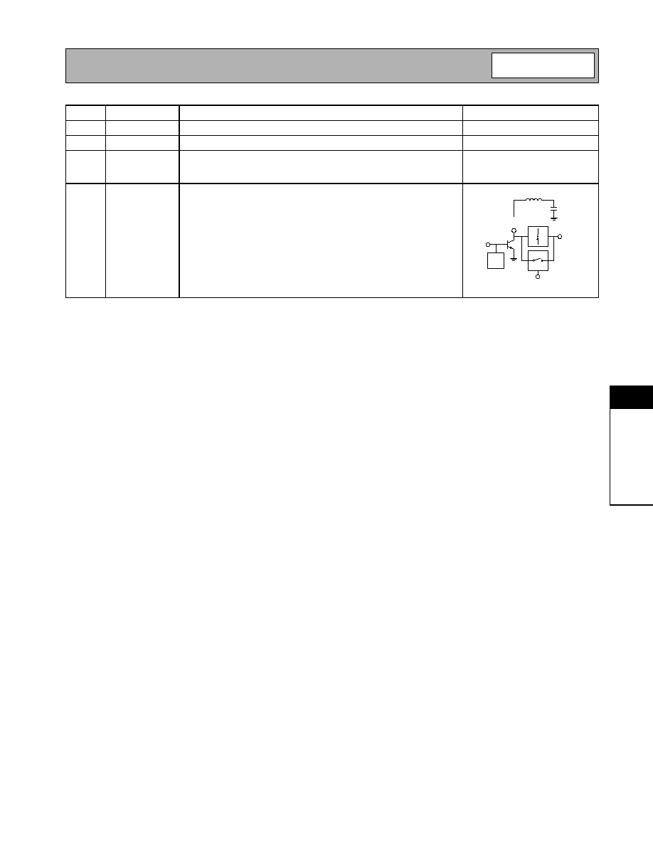
Pin
Function
Description
Interface Schematic
1
GAIN SEL
LNA gain control. When GAIN SEL is > V
CC
- 300mV, LNA gain is at 10
dB. When GAIN SEL is <300mV, the LNA gain is -6dB.
See pin 16.
2
LNA IN
This pin is NOT internally DC blocked. An external blocking capacitor
must be provided if the pin is connected to a device with DC present. If
a blocking capacitor is required, a value of 2pF is recommended.
See pin 16.
3
PD
The power enable pin. When PD is > V
CC
- 300mV, the part is biased
on. When PD is <300mV, then the part is turned off and typically draws
less than 1
µ
A.
4
VCC1
Supply voltage for bias circuits and logic control. A 10pF external
bypass capacitor is required and an additional 0.01
µ
F is required if no
other low frequency bypass capacitors are nearby. The trace length
between the pin and the bypass capacitors should be minimized. The
ground side of the bypass capacitors should connect immediately to
ground plane.
5
VCC2
Supply voltage for LO_Buffer. A 10pF bypass capacitor is required and
an additional 0.01
µ
F is required if there is no other low frequency
bypass capacitor in the area. The trace length between the pin and the
bypass capacitors should be minimized. The ground side of the bypass
capacitors should connect immediately to ground plane.
See pin 8.
6
MIXOUT-
The inverting open collector output of the mixer. This pin needs to be
externally biased and DC isolated from other parts of the circuit. This
output can drive a Balun, with MIXOUT+, to convert to unbalanced to
drive a SAW filter. The Balun can be either broadband (transformer) or
narrowband (discrete LC matching). Alternatively, MIXOUT+ may be
used alone to drive a SAW single-ended, with an RF choke (high Z at
IF) from VCC to MIXOUT-.
7
MIXOUT+
The non-inverting open collector output of the mixer. This pin needs to
be externally biased and DC isolated from other parts of the circuit.
This output can drive a Balun, with MIXOUT+, to convert to unbalanced
to drive a SAW filter. The Balun can be either broadband (transformer)
or narrowband (discrete LC matching). Alternatively, MIXOUT+ may be
used alone to drive a SAW single-ended, with an RF choke (high Z at
IF) from VCC to MIXOUT+.
See pin 6.
8
LO IN
LO input pin. This input needs a DC blocking cap. External matching is
recommended to 50
.
9
RX EN
This control pin allows the mixer output pins to be put into a high
impedance state. This allows the transmit signal path to share the
same IF filter as the receiver.
10
VCC3
Supply voltage for mixer preamp.
See pin 12.
11
GND3
Ground pin for mixer preamp. This lead inductance should be kept
small.
See pin 12.
12
MIX IN
Mixer RF Input port. This pin is NOT internally DC blocked. An external
blocking capacitor must be provided if the pin is connected to a device
with DC present. A value of >22pF is recommended. To minimize the
noise figure it is recommended to have a bandpass filter before this
input. This will prevent the noise at the image frequency from being
converted to the IF.
MIX OUT+
MIX OUT-
LO IN
VCC2
VCC3
GND3
MIX IN
8-57
RF2444
Rev A3 010717
8
F
R
O
N
T
-
E
NDS
Pin
Function
Description
Interface Schematic
13
NC
14
NC
15
LNA OUT
RF signal output for external 50
filtering.The use of a filter here is
optional but does provide for lower noise floor and better out-of-band
rejection.
See pin 16.
16
VCC4
Supply voltage for the LNA. This pin should be bypassed with a 10 pF
capacitor to ground as close to the pin as possible. The shunt induc-
tance from this pin to ground via the supply decoupling must be tuned
to match the LNA output to 50
at the desired operating frequency.
P2
LNA IN
BIAS
VCC4
P1
GAIN SEL
P15
LNA OUT
EXTERNAL
DECOUPLING
Microstrip
-16 dB

8-58
RF2444
Rev A3 010717
8
F
R
O
N
T
-
E
NDS
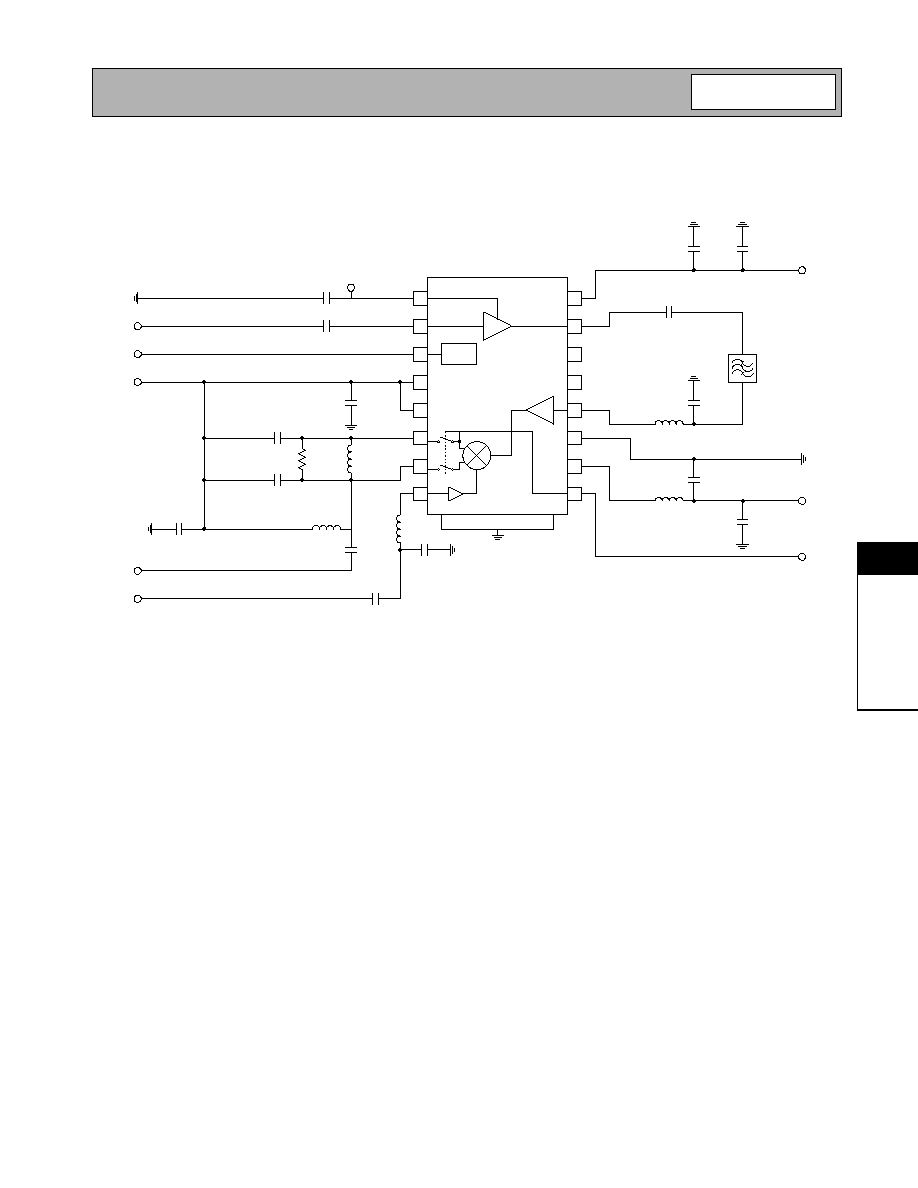
Theory of Operation
RX
15 dB Gain
IL = 3-4 dB
2.4 to 2.483 GHz
LNA
Dual Gain Modes
-5 dB and +10 dB
Gain
Select
RF2444
SSOP-16 EPP
Filter
2.4 to 2.483 GHz
SAW
IL = 10 dB max
RX
TX
15 dB
15 dB
IF Amp
-15 dB to 35 dB Gain
DATA Q
OUT Q
RSSI
DATA I
OUT I
Filter
Filter
Selectable LPF
TX
I INPUT
Q INPUT
15 dB Gain
Range
+45°
-45°
IL = 3-4 dB
2.4 to 2.483 GHz
10 dBm
PA Driver
RF2938
TQFP-48 EPP
VGC1
VGC2
Base Band Amp.
Active Selectable LPF
(f
C
= 1 MHz to 40 MHz)
0-30 dB Gain
RF Micro Devices
2.4 GHz ISM Chipset
23 dBm or 33 dBm
External PA
RF2126
IF
VCO
RF
VCO
RF2517
SSOP-28
Dual
Frequency
Synthesizer
Discrete
Pin Diode
Figure 1. Entire Chipset Functional Block Diagram
The RF2444 contains the LNA/Mixer for this chipset.
The LNA is made from two stages including a common
emitter amplifier stage with a power gain of 13dB and
an attenuator which has an insertion loss of 3dB in
high gain mode, and 17dB in low gain mode. The
attenuator was put after the LNA so that system noise
figure degradation would be minimized. A single gain
stage was used prior to the image filter to maximize
IP3 which minimizes the risk of large out-of-bad signals
jamming the desired signal.
The mixer on the RF2444 is also two stages. The first
stage is a common emitter amp used to boost the total
power gain prior to the lossy SAW filter, to convert to a
differential signal to the input of the mixer, and to
improve the noise figure of the mixer. The second
stage is a double balanced mixer whose output is dif-
ferential open collector. It is recommended that a "cur-
rent combiner" is used (as shown in figure 2) at the
mixer output to maximize conversion gain, but other
loads can also be used. The current combiner is used
to do a differential to single ended conversion for the
SAW filter. C1, C2 and L1 are used to tune the circuit
for a specific IF frequency. L2 is a choke to supply DC
current to the mixer that is also used as a tuning ele-
ment, along with C3, to match to the SAW filter's input
impedance. RL is the SAW filter's input impedance.
The mixer power conversion gain is +19dB when R1 is
set to 1k
. The conversion gain can be adjusted up
~5dB or down ~7dB by changing the value of R1.
Once R1 is chosen, L2 and C3 can be used to tune the
output for the SAW filter.
The cascaded power gain of the LNA/Mixer is 29dB,
which after insertion loss in the image filter (~3dB) and
IF SAW filter (~10dB), still gives 16dB of gain prior to
the IF amps. Because of this, the noise figure of the IF
amps should not significantly degrade system noise
figure.
The LNA input should be matched for a good return
loss for optimum gain and noise figure. To allow the
designer to match each of these ports, 2-port s-param-
eter data is available for the LNA, and 1-port data is
available for MIXER IN and LO IN.
L1
R1
C1
C2 L2
C3
RL
VCC
OUT
Open Collector
Mixer Output
Figure 2. Current Combiner for Mixer Load
8-59
RF2444
Rev A3 010717
8
F
R
O
N
T
-
E
NDS
Application Schematic
1
2
3
4
5
6
7
8
16
15
14
13
12
11
10
9
LNA
MIXER
RF AMP
Bias
Circuits
DIE FLAG (17)
22 pF
GS
2 pF
CE
22 nF
VCC1
VCC2
220 nH
1k
3 pF
3 pF
4 pF
47 nH
22 nF
6.8 nH
C2
1 pF
10 pF
OE
2.7 nH
22 nF
VCC3
VCC4
22 nF
4.7 nH
1.5 pF
3 pF
LNA IN
IF OUT
LO IN
4.7
µ
F
Bandpass
Filter
4.7
µ
F
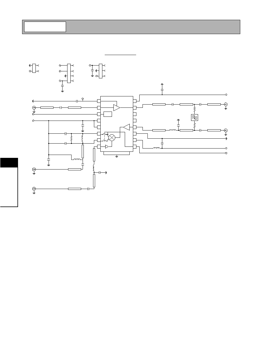
8-60
RF2444
Rev A3 010717
8
F
R
O
N
T
-
E
NDS
Evaluation Board Schematic
(Download Bill of Materials from www.rfmd.com.)
1
2
3
4
5
6
7
8
16
15
14
13
12
11
10
9
LNA
MIXER
RF AMP
Bias
Circuits
DIE FLAG (17)
C10
22 pF
GS
50
µ
strip
C1
2 pF
50
µ
strip
J1
LNA IN
CE
C11
22 nF
VCC1
VCC2
L2
220 nH
R1
1k
C3
3 pF
C4
3 pF
50
µ
strip
C19
4 pF
L3
47 nH
50
µ
strip
J3
IF OUT
C14
22 nF
L1
6.8 nH
50
µ
strip
C2
1 pF
50
µ
strip
C5
10 pF
50
µ
strip
J2
LO IN
OE
L7
2.7 nH
C9
22 nF
VCC3
VCC4
C6
22 nF
50
µ
strip
L5
4.7 nH
50
µ
strip
C8
1.5 pF
*C16
22 pF
50
µ
strip
J5
MIX IN
50
µ
strip
C7
3 pF
50
µ
strip
*C15
22 pF
50
µ
strip
J4
LNA OUT
*R2
0
*R3
0
GS
CE
GND
VCC4
C18
4.7
µ
F
P2
1
2
3
4
P1
1
2
GND
VCC1, VCC2
OE
GND
VCC3
C17
4.7
µ
F
P3
1
2
3
2444400 Rev. A
*For cascaded configuration, jumpers R2 and R3
need to be installed with C15 and C16 taken out.
Bandpass
Filter
*To test LNA and Mixer separately remove R2 and
R3, and fit C15 and C16.

8-61
RF2444
Rev A3 010717
8
F
R
O
N
T
-
E
NDS
Evaluation Board Layout
Board Thickness 0.031", Board Material FR-4
NOTE: In the following charts, all cascaded data measured with a bandpass filter inserted between LNA OUT and MIX
IN, having cut frequencies: f
L
=2400 MHz, f
M
=2484 MHz, and insertion loss= 1.2 dB.

8-62
RF2444
Rev A3 010717
8
F
R
O
N
T
-
E
NDS
LNA + Mixer Gain versus VCC (2.45 GHz),
Attenuator Off
25.0
26.0
27.0
28.0
29.0
30.0
31.0
32.0
33.0
2.7
3.0
3.3
3.6
VCC
Gain
(dB)
-40C Gain
25C Gain
85C Gain
LNA + Mixer IIP3 versus VCC (2.45 GHz),
Attenuator Off
-31.0
-30.0
-29.0
-28.0
-27.0
-26.0
-25.0
-24.0
2.7
3.0
3.3
3.6
VCC
IIP3
(dBm)
-40C IIP3
25C IIP3
85C IIP3
LNA + Mixer Gain versus RF Frequency (3.3 V),
Attenuator Off
26.00
27.00
28.00
29.00
30.00
31.00
32.00
33.00
34.00
2.40
2.45
2.50
RF Frequency (GHz)
Gain
(dB)
-40C Gain
25C Gain
85C Gain
LNA + Mixer IIP3 versus RF Frequency (3.3V),
Attenuator Off
-32.00
-31.00
-30.00
-29.00
-28.00
-27.00
-26.00
-25.00
-24.00
2.40
2.45
2.50
RF Frequency (GHz)
IIP3
(dBm)
-40C IIP3
25C IIP3
85C IIP3
LNA + Mixer Gain versus VCC (2.45 GHz),
Attenuator On
9.0
9.5
10.0
10.5
11.0
11.5
12.0
12.5
13.0
13.5
14.0
2.7
3.0
3.3
3.6
VCC
Gain
(dB)
-40C Gain
25C Gain
85C Gain
LNA + Mixer IIP3 versus VCC (2.45 GHz),
Attenuator On
-10.4
-10.2
-10.0
-9.8
-9.6
-9.4
-9.2
-9.0
-8.8
-8.6
2.7
3.0
3.3
3.6
VCC
IIP3
(dBm)
-40C IIP3
25C IIP3
85C IIP3

8-63
RF2444
Rev A3 010717
8
F
R
O
N
T
-
E
NDS
LNA + Mixer Gain versus RF Frequency (3.3 V),
Attenuator On
9.00
9.50
10.00
10.50
11.00
11.50
12.00
12.50
13.00
13.50
14.00
14.50
15.00
2.40
2.45
2.50
RF Frequency (GHz)
Gain
(dB)
-40C Gain
25C Gain
85C Gain
LNA + Mixer IIP3 versus RF Frequency (3.3 V),
Attenuator On
-11.00
-10.50
-10.00
-9.50
-9.00
-8.50
-8.00
-7.50
-7.00
2.40
2.45
2.50
RF Frequency (GHz)
IIP3
(dBm)
-40C IIP3
25C IIP3
85C IIP3
LNA + Mixer SSB Noise Figure versus VCC (2.45 GHz),
Attenuator Off
4.4
4.6
4.8
5.0
5.2
5.4
5.6
2.7
3.0
3.3
3.6
VCC
SSB
Noise
Figure
(
dB)
25C NF
85C NF
-40C NF
LNA + Mixer SSB Noise Figure versus
RF Frequency (3.3 V), Attenuator Off
3.00
3.50
4.00
4.50
5.00
5.50
2.40
2.45
2.50
RF Frequency (GHz)
SSB
Noise
Figure
(
dB)
25C NF
85C NF
-40C NF
LNA + Mixer SSB Noise Figure versus VCC (2.45 GHz),
Attenuator On
17.8
18.0
18.2
18.4
18.6
18.8
19.0
19.2
19.4
19.6
19.8
2.7
3.0
3.3
3.6
VCC
SSB
Noise
Figure
(
dB)
25C NF
85C NF
-40C NF
LNA + Mixer SSB Noise Figure versus
RF Frequency (3.3 V), Attenuator On
13.00
14.00
15.00
16.00
17.00
18.00
19.00
20.00
2.40
2.45
2.50
RF Frequency (GHz)
SSB
Noise
Figure
(
dB)
25C NF
85C NF
-40C NF

8-64
RF2444
Rev A3 010717
8
F
R
O
N
T
-
E
NDS
LNA + Mixer Gain versus IF Frequency (3.3 V)
26.0
27.0
28.0
29.0
30.0
31.0
32.0
0.0
50.0
100.0
150.0 200.0
250.0
300.0
350.0
400.0
450.0
500.0
IF Frequency (MHz)
Gain
(dB)
Gain
LNA + Mixer IIP3 versus IF Frequency (3.3 V)
-31.0
-30.0
-29.0
-28.0
-27.0
-26.0
-25.0
-24.0
-23.0
0.0
50.0
100.0 150.0
200.0
250.0
300.0 350.0 400.0
450.0 500.0
IF Frequency (MHz)
IIP3
(dBm)
IIP3
LNA I
CC
versus VCC
(PD = 1, RX EN = 0)
10.9
11.1
11.3
11.5
11.7
11.9
12.1
12.3
12.5
12.7
2.7
3.0
3.3
3.6
VCC
I
CC
(mA)
25C LNA Icc
85C LNA Icc
-40C LNA Icc
Total I
CC
versus VCC
(PD = 1, RX EN = 1)
18.0
18.5
19.0
19.5
20.0
20.5
21.0
2.7
3.0
3.3
3.6
VCC
I
CC
(mA)
25C Total Icc
85C Total Icc
-40C Total Icc
Isolation
-48.00
-43.00
-38.00
-33.00
-28.00
-23.00
-18.00
-13.00
2.12
2.17
2.22
LO Frequency (GHz)
Isolation
(
dB)
LO-mixin
LO-LNAin
LNAin-LNAout
LO-IFout

8-65
RF2444
Rev A3 010717
8
F
R
O
N
T
-
E
NDS
LNA Gain versus VCC (2.45 GHz),
Attenuator Off
9.5
9.6
9.7
9.8
9.9
10.0
10.1
10.2
10.3
10.4
10.5
2.7
3.0
3.3
3.6
VCC
Gain
(dB)
-40C Gain
25C Gain
85C Gain
LNA IIP3 versus VCC (2.45 GHz),
Attenuator Off
-2.8
-2.7
-2.6
-2.5
-2.4
-2.3
-2.2
-2.1
-2.0
2.7
3.0
3.3
3.6
VCC
IIP3
(dBm)
-40C IIP3
25C IIP3
85C IIP3
LNA Gain versus VCC (2.45 GHz),
Attenuator On
-5.6
-5.4
-5.2
-5.0
-4.8
-4.6
-4.4
-4.2
-4.0
2.7
3.0
3.3
3.6
VCC
Gain
(dB)
-40C Gain
25C Gain
85C Gain
LNA IIP3 versus VCC (2.45 GHz),
Attenuator On
-3.0
-2.8
-2.6
-2.4
-2.2
-2.0
-1.8
2.7
3.0
3.3
3.6
VCC
IIP3
(dBm)
-40C IIP3
25C IIP3
85C IIP3
LNA Gain versus RF Frequency (3.3 V),
Attenuator Off
9.70
9.80
9.90
10.00
10.10
10.20
10.30
10.40
10.50
10.60
10.70
2.40
2.45
2.50
RF Frequency (GHz)
Gain
(dB)
-40C Gain
25C Gain
85C Gain
LNA IIP3 versus RF Frequency (3.3 V),
Attenuator Off
-3.50
-3.00
-2.50
-2.00
-1.50
-1.00
-0.50
0.00
2.40
2.45
2.50
RF Frequency (GHz)
IIP3
(dBm)
-40C IIP3
25C IIP3
85C IIP3

8-66
RF2444
Rev A3 010717
8
F
R
O
N
T
-
E
NDS
LNA Gain versus RF Frequency (3.3 V),
Attenuator On
-5.50
-5.30
-5.10
-4.90
-4.70
-4.50
-4.30
-4.10
-3.90
-3.70
2.40
2.45
2.50
RF Frequency (GHz)
Gain
(dB)
-40C Gain
25C Gain
85C Gain
LNA IIP3 versus RF Frequency (3.3 V),
Attenuator On
-2.90
-2.80
-2.70
-2.60
-2.50
-2.40
-2.30
-2.20
-2.10
-2.00
-1.90
2.40
2.45
2.50
RF Frequency (GHz)
IIP3
(dBm)
-40C IIP3
25C IIP3
85C IIP3
LNA Noise Figure versus VCC (2.45 GHz),
Attenuator Off
2.10
2.12
2.14
2.16
2.18
2.20
2.22
2.24
2.26
2.28
2.30
2.32
2.70
3.00
3.30
3.60
VCC
Noise
Figure
(
dB)
-40C NF
25C NF
85C NF
LNA Noise Figure versus RF Frequency (3.3 V),
Attenuator Off
2.10
2.15
2.20
2.25
2.30
2.35
2.40
2.45
2.50
2.40
2.45
2.50
RF Frequency (GHz)
Noise
Figure
(
dB)
-40C NF
25C NF
85C NF
LNA Noise Figure versus VCC (2.45 GHz),
Attenuator On
5.0
5.5
6.0
6.5
7.0
7.5
8.0
8.5
9.0
2.7
3.0
3.3
3.6
VCC
Noise
Figure
(
dB)
-40C NF
25C NF
85C NF
LNA Noise Figure versus RF Frequency (3.3 V),
Attenuator On
5.00
5.50
6.00
6.50
7.00
7.50
8.00
8.50
9.00
2.40
2.45
2.50
RF Frequency (GHz)
Noise
Figure
(
dB)
-40C NF
25C NF
85C NF

8-67
RF2444
Rev A3 010717
8
F
R
O
N
T
-
E
NDS
Mixer Gain versus VCC (2.45 GHz)
16.0
17.0
18.0
19.0
20.0
21.0
22.0
2.7
3.0
3.3
3.6
VCC
Gain
(dB)
-40C Gain
25C Gain
85C Gain
Mixer IIP3 versus VCC (2.45 GHz)
-18.0
-17.5
-17.0
-16.5
-16.0
-15.5
-15.0
-14.5
2.7
3.0
3.3
3.6
VCC
IIP3
(dBm)
-40C IIP3
25C IIP3
85C IIP3
Mixer Gain versus RF Frequency (3.3 V)
16.00
17.00
18.00
19.00
20.00
21.00
22.00
2.40
2.45
2.50
RF Frequency (GHz)
Gain
(dB)
-40C Gain
25C Gain
85C Gain
Mixer IIP3 versus RF Frequency (3.3 V)
-18.50
-18.00
-17.50
-17.00
-16.50
-16.00
-15.50
-15.00
2.40
2.45
2.50
RF Frequency (GHz)
IIP3
(dBm)
-40C IIP3
25C IIP3
85C IIP3
Mixer SSB Noise Figure versus VCC (2.45 GHz)
10.0
10.5
11.0
11.5
12.0
12.5
13.0
13.5
2.7
3.0
3.3
3.6
VCC
SSB
Noise
Figure
(
dB)
-40C NF
25C NF
85C NF
Mixer SSB Noise Figure versus RF Frequency (3.3 V)
7.00
8.00
9.00
10.00
11.00
12.00
13.00
2.40
2.45
2.50
RF Frequency (GHz)
SSB
Noise
Figure
(
dB)
-40C NF
25C NF
85C NF

8-68
RF2444
Rev A3 010717
8
F
R
O
N
T
-
E
NDS
Mixer Gain versus LO Amplitude
(VCC = 3.3 V, RF Frequency = 2.45 GHz)
14
15
16
17
18
19
20
-24
-22
-20
-18 -16
-14 -12
-10
-8
-6
-4
-2
0
2
4
6
LO Amplitude (dBm)
Gain
(dB)
Gain
Mixer IIP3 versus LO Amplitude
(VCC = 3.3 V, RF Frequency = 2.45 GHz)
-20
-19
-18
-17
-16
-15
-14
-24 -22
-20
-18 -16 -14
-12
-10
-8
-6
-4
-2
0
2
4
6
LO Amplitude (dBm)
IIP3
(dBm)
IIP3