This product conforms to specifications per the terms of the Ramtron
Ramtron International Corporation
standard warranty. Production processing does not necessarily in-
1850 Ramtron Drive, Colorado Springs, CO 80921
clude testing of all parameters.
(800) 545-FRAM, (719) 481-7000, Fax (719) 481-7058
www.ramtron.com
Rev 2.0
Dec 2002
1 of 12
FM18L08
256Kb Bytewide FRAM Memory
Features
256K bit Ferroelectric Nonvolatile RAM
· Organized as 32,768 x 8 bits
· 10 year Data Retention
· Unlimited Read/Write Cycles
· NoDelayTM Writes
· Advanced High-Reliability Ferroelectric Process
Superior to Battery-Backed SRAM
· No Battery Concerns
· Monolithic Reliability
· True surface mount solution, no rework steps
· Superior for moisture, shock, and vibration
· Resistant to negative voltage undershoots
SRAM & EEPROM Compatible
· JEDEC 32Kx8 SRAM & EEPROM pinout
· 70 ns Access Time
· 140 ns Cycle Time
Low Power Operation
· 3.0V to 3.65V Operation
· 15 mA Active Current
· 15 µA Standby Current
Industry Standard Configuration
· Industrial Temperature -40° C to +85° C
· 28-pin SOIC or DIP
Description
The FM18L08 is a 256-kilobit nonvolatile memory
employing an advanced ferroelectric process. A
ferroelectric random access memory or FRAM is
nonvolatile and reads and writes like a RAM. It
provides data retention for 10 years while eliminating
the reliability concerns, functional disadvantages and
system design complexities of battery-backed SRAM
(BBSRAM). Fast write timing and high write
endurance make FRAM superior to other types of
nonvolatile memory.
In-system operation of the FM18L08 is very similar
to other RAM based devices. Read cycle and write
cycle times are equal. The FRAM memory, however,
is nonvolatile due to its unique ferroelectric memory
process. Unlike BBSRAM, the FM18L08 is a truly
monolithic nonvolatile memory. It provides the same
functional benefits of a fast write without the
disadvantages associated with modules and batteries
or hybrid memory solutions.
These capabilities make the FM18L08 ideal for
nonvolatile memory applications requiring frequent
or rapid writes in a bytewide environment. The
availability of a surface-mount package improves the
manufacturability of new designs, while the DIP
package facilitates simple design retrofits. Device
specifications are guaranteed over a temperature
range of -40°C to +85°C.
Pin Configuration
A14
A12
A7
A6
A5
A4
A3
A2
A1
A0
DQ0
DQ1
DQ2
VSS
DQ3
DQ4
DQ5
DQ6
DQ7
CE
A10
OE
A11
A9
A8
A13
WE
VDD
1
2
3
4
5
6
7
8
9
10
11
12
13
14
28
27
26
25
24
23
22
21
20
19
18
17
16
15
Ordering Information
FM18L08-70-S
70 ns access, 28-pin SOIC
FM18L08-70-P
70 ns access, 28-pin DIP
FM18L08
Rev 2.0
Dec 2002
2 of 12
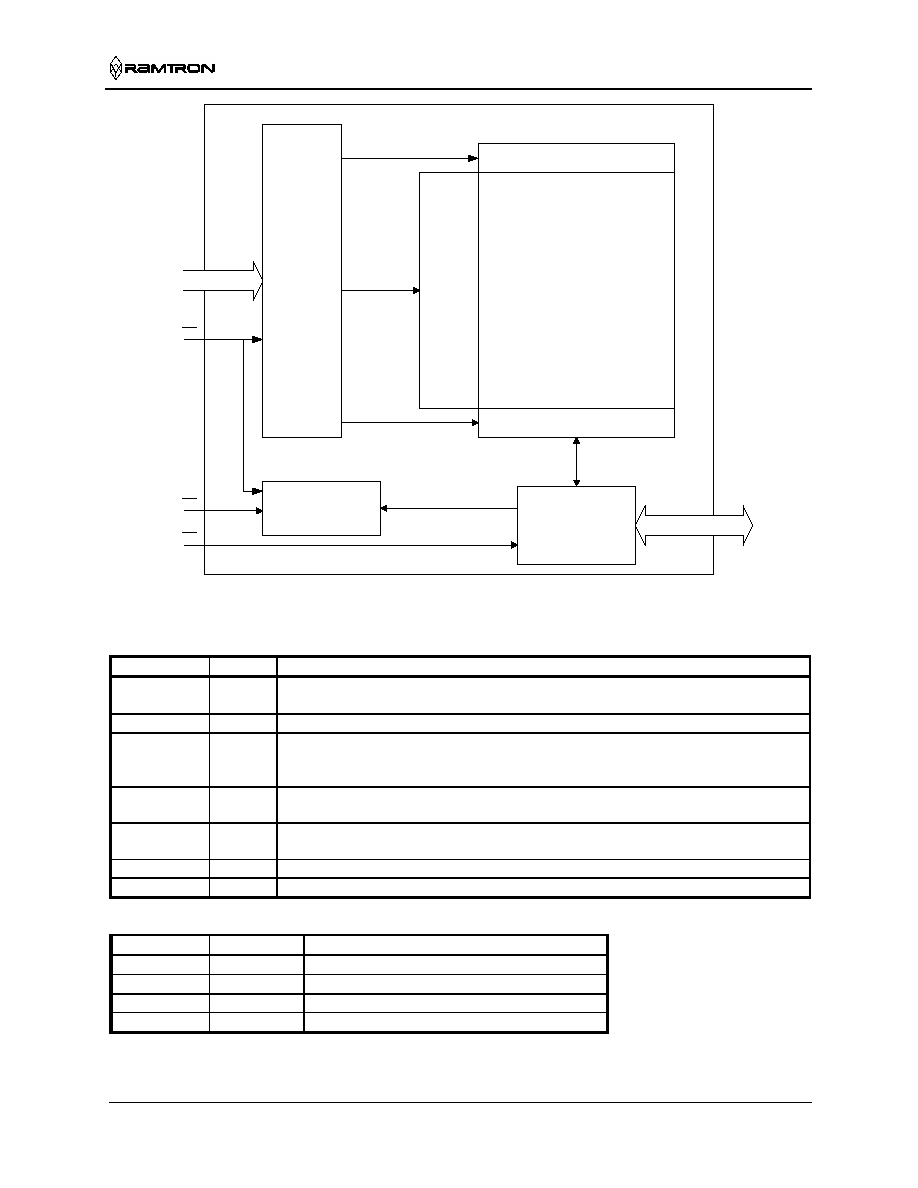
Address
Latch
A0-A14
CE
Control
Logic
WE
Row
Decoder
Block Decoder
Column Decoder
A0-A7
A8-A9
A10-A14
I/O Latch
Bus Driver
OE
32,768 x 8 FRAM Array
DQ0-7
Figure 1. Block Diagram
Pin Description
Pin Name
Type
Pin Description
A0-A14
Input
Address: The 15 address lines select one of 32,768 bytes in the FRAM array. The
address value is latched on the falling edge of /CE.
DQ0-7
I/O
Data: 8-bit bi-directional data bus for accessing the FRAM array.
/CE
Input
Chip Enable. /CE selects the device when low. Asserting /CE low causes the address
to be latched internally. Address changes that occur after /CE goes low will be
ignored until the next falling edge occurs.
/OE
Input
Output Enable: Asserting /OE low causes the FM18L08 to drive the data bus when
valid data is available. Deasserting /OE high causes the DQ pins to be tri-stated.
/WE
Input
Write Enable: Asserting /WE low causes the FM18L08 to write the contents of the
data bus to the address location latched by the falling edge of /CE.
VDD Supply
Supply
Voltage
VSS Supply
Ground
Functional Truth Table
/CE /WE
Function
H X
Standby/Precharge
X
Latch Address (and Begin Write if /WE=low)
L H
Read
L
Write
Note: The /OE pin controls only the DQ output buffers.

FM18L08
Rev 2.0
Dec 2002
3 of 12
Overview
The FM18L08 is a bytewide FRAM memory. The
memory array is logically organized as 32,768 x 8
and is accessed using an industry standard parallel
interface. All data written to the part is immediately
nonvolatile with no delay. Functional operation of the
FRAM memory is the same as SRAM type devices,
except the FM18L08 requires a falling edge of /CE to
start each memory cycle.
Memory Operation
Users access 32,768 memory locations each with 8
data bits through a parallel interface. The cycle time
is the same for read and write memory operations.
This simplifies memory controller logic and timing
circuits. Likewise the access time is the same for read
and write memory operations. When /CE is
deasserted high, a precharge operation begins, and is
required of every memory cycle. Thus unlike SRAM,
the access and cycle times are not equal. Writes occur
immediately at the end of the access with no delay.
Unlike an EEPROM, it is not necessary to poll the
device for a ready condition since writes occur at bus
speed.
Note that the FM18L08 contains a limited low
voltage write protection circuit. This will prevent
access when V
DD
is much lower than the specified
operating range. It is still the user's responsibility to
ensure that V
DD
is within data sheet tolerances to
prevent incorrect operation.
The FM18L08 is designed to operate in a manner
similar to other bytewide memory products. For users
familiar with SRAM, the performance is comparable
but the bytewide interface operates in a slightly
different manner as described below. For users
familiar with EEPROM, the obvious differences
result from the higher write performance of FRAM
technology including NoDelay writes and from
unlimited write endurance.
Read Operation
A read operation begins on the falling edge of /CE.
At this time, the address bits are latched and a
memory cycle is initiated. Once started, a full
memory cycle must be completed internally
regardless of the state of /CE. Data becomes available
on the bus after the access time has been satisfied.
After the address has been latched, the address value
may be changed upon satisfying the hold time
parameter. Unlike an SRAM, changing address values
will have no effect on the memory operation after the
address is latched.
The FM18L08 drives the data bus when /OE is
asserted to a low state. If /OE is asserted after the
memory access time has been satisfied, the data bus
will be driven with valid data. If /OE is asserted prior
to completion of the memory access, the data bus will
be driven when valid data is available. This feature
minimizes supply current in the system by eliminating
transients caused by invalid data being driven onto
the bus. When /OE is inactive the data bus will
remain tri-stated.
Write Operation
Writes operations require the same time as reads. The
FM18L08 supports both /CE- and /WE-controlled
write cycles. In all cases, the address is latched on the
falling edge of /CE.
In a /CE-controlled write, the /WE signal is asserted
prior to beginning the memory cycle. That is, /WE is
low when /CE falls. In this case, the device begins the
memory cycle as a write. The FM18L08 will not
drive the data bus regardless of the state of /OE.
In a /WE-controlled write, the memory cycle begins
on the falling edge of /CE. The /WE signal falls after
the falling edge of /CE. Therefore, the memory cycle
begins as a read. The data bus will be driven
according to the state of /OE until /WE falls. The
timing of both /CE- and /WE-controlled write cycles
is shown in the electrical specifications.
Write access to the array begins asynchronously after
the memory cycle is initiated. The write access
terminates on the rising edge of /WE or /CE,
whichever is first. Data set-up time, as shown in the
electrical specifications, indicates the interval during
which data cannot change prior to the end of the write
access.
Unlike other truly nonvolatile memory technologies,
there is no write delay with FRAM. Since the read
and write access times of the underlying memory are
the same, the user experiences no delay through the
bus. The entire memory operation occurs in a single
bus cycle. Therefore, any operation including read or
write can occur immediately following a write. Data
polling, a technique used with EEPROMs to
determine if a write is complete, is unnecessary.
Precharge Operation
The precharge operation is an internal condition
where the state of the memory is prepared for a new
access. All memory cycles consist of a memory
access and a precharge. The precharge is user

FM18L08
Rev 2.0
Dec 2002
4 of 12
initiated by taking the /CE signal high or inactive. It
must remain high for at least the minimum precharge
timing specification.
The user dictates the beginning of this operation since
a precharge will not begin until /CE rises. However,
the device has a maximum /CE low time specification
that must be satisfied.
Applications
As a true nonvolatile RAM, the FM18L08 fits into
many diverse applications. Clearly, its monolithic
nature and high performance make it superior to
battery-backed SRAM in many applications.
Unlimited endurance allows the FM18L08 to be used
in applications that could not take advantage of the
previous generation of RAM products. This
applications guide is intended to facilitate the
transition from BBSRAM to FRAM. It is divided into
two parts. First is a treatment of the advantages of
FRAM memory compared with battery-backed
SRAM. Second is a design guide, which highlights
design considerations that should be reviewed in both
retrofit and new design situations.
FRAM Advantages
Although battery-backed SRAM is a mature and
established solution, it has many weaknesses. These
stem directly or indirectly from the presence of the
battery. FRAM uses an inherently nonvolatile storage
mechanism that requires no battery. It therefore
eliminates these weaknesses. The major
considerations in upgrading to FRAM are as follows.
Construction Issues
1. Cost
The cost of both the component and the
manufacturing overhead of battery-backed SRAM is
high. FRAM with its monolithic construction is
inherently a lower cost solution. In addition, there is
no `built-in' rework step required for battery
attachment when using surface mount parts.
Therefore assembly is streamlined and more cost
effective. In the case of DIP battery-backed modules,
the user is constrained to through-hole assembly
techniques and a board wash using no water.
2. Humidity
A typical battery-backed SRAM module is qualified
at 60ş C, 90% Rh, but under no bias and no pressure.
These conditions are chosen because multi-
component assemblies are vulnerable to moisture and
dirt. FRAM is qualified using HAST highly
accelerated stress test. This requires 120ş C at 85%
Rh, 24.4 psia at VDD.
3. System reliability
Data integrity must be questioned when using a
battery-backed SRAM. They are inherently
vulnerable to shock and vibration. If the battery
contact comes loose, data will be lost. In addition a
negative voltage, even a momentary undershoot, on
any pin of a battery-backed SRAM can cause data
loss. The negative voltage causes current to be drawn
directly from the battery. These momentary short
circuits can greatly weaken a battery and reduce its
capacity over time. In general, there is no way to
monitor the lost battery capacity. Should an
undershoot occur in a battery backed system during a
power down, data can be lost immediately.
4. Space
Certain disadvantages of battery-backed SRAM, such
as susceptibility to shock, can be reduced by using the
old fashioned DIP module. However, this alternative
takes up board space, height, and dictates through-
hole assembly. FRAM offers a true surface-mount
solution that uses 25% of the board space. No multi-
piece assemblies, no connectors, and no modules. A
real nonvolatile RAM is finally available!
Direct Battery Issues
5. Field maintenance
No matter how mature batteries become, they are a
built-in maintenance problem. They eventually must
be replaced. Despite long life projections, it is
impossible to know if any individual battery will last
considering all of the factors that can degrade them.
6. Environmental
Lithium batteries are widely regarded as an
environmental problem. They are a potential fire
hazard and proper disposal can be a burden. In
addition, shipping of lithium batteries may be
restricted.
7. Style
Backing up an SRAM with a battery is an old-
fashioned approach. In many cases, such modules are
the only through-hole component in sight. FRAM is
the latest memory technology and it is changing the
way systems are designed.
FM18L08
Rev 2.0
Dec 2002
5 of 12
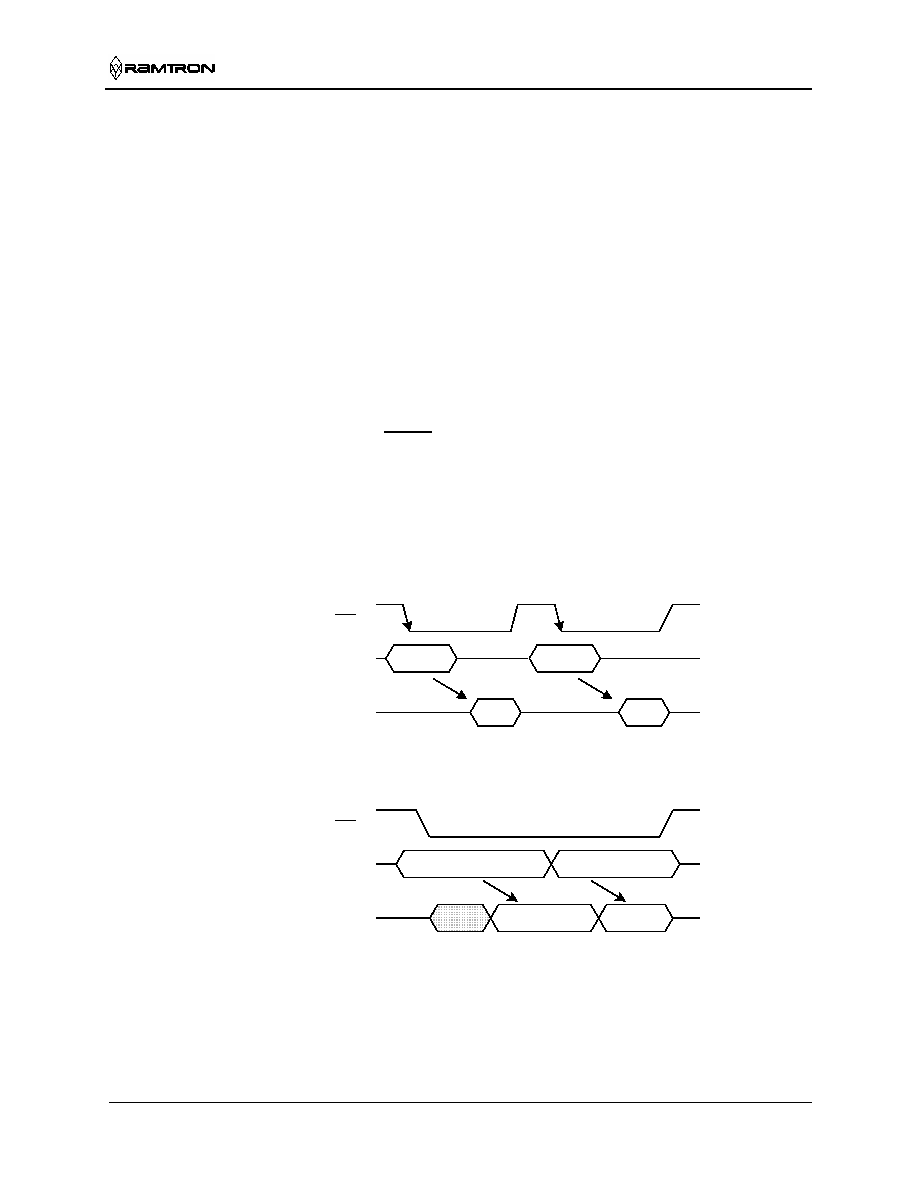
FRAM Design Considerations
When designing with FRAM for the first time, users
of SRAM will recognize a few minor differences.
First, bytewide FRAM memories latch each address
on the falling edge of chip enable. This allows the
address bus to change after starting the memory
access. Since every access latches the memory
address on the falling edge of /CE, users cannot
ground it as they might with SRAM.
Users who are modifying existing designs to use
FRAM should examine the memory controller for
timing compatibility of address and control pins.
Each memory access must be qualified with a low
transition of /CE. In many cases, this is the only
change required. An example of the signal
relationships is shown in Figure 2 below. Also shown
is a common SRAM signal relationship that will not
work for the FM18L08.
The reason for /CE to strobe for each address is two-
fold: it latches the new address and creates the
necessary precharge period while /CE is high.
A second design consideration relates to the level of
V
DD
during operation. Battery-backed SRAMs are
forced to monitor V
DD
in order to switch to battery
backup. They typically block user access below a
certain V
DD
level in order to prevent loading the
battery with current demand from an active SRAM.
The user can be abruptly cut off from access to the
nonvolatile memory in a power down situation with
no warning or indication.
FRAM memories do not need this system overhead.
The memory will not block access at any V
DD
level.
The user, however, should prevent the processor from
accessing memory when V
DD
is out-of-tolerance. The
common design practice of holding a processor in
reset when V
DD
drops is adequate; no special
provisions must be taken for FRAM design.
Address 1
Address 2
Data 1
Data 2
Valid Memory Signaling Relationship
CE
Address
Data
FRAM
signaling
Address 2
Data 1
CE
Address
Data
SRAM
signaling
Invalid Memory Signaling Relationship
Address 1
Data 2
Figure 2. Memory Address Relationships