
Philips
Semiconductors
SSTL16877
14-bit SSTL_2 registered driver with
differential clock inputs
Product specification
Supersedes data of 2000 Apr 11
2000 Apr 20
INTEGRATED CIRCUITS
Philips Semiconductors
Product specification
SSTL16877
14-bit SSTL_2 registered driver with
differential clock inputs
2
2000 Apr 20
853-2198 23523
FEATURES
À
Stub-series terminated logic for 2.5 V VDDQ (SSTL_2)
À
Optimized for DDR (Double Data Rate) SDRAM applications
À
Supports SSTL_2 signal inputs and outputs
À
Flow-through architecture optimizes PCB layout
À
Meets SSTL_2 class I and class II specifications
À
Latch-up protection exceeds 500mA per JEDEC Std 17
À
ESD protection exceeds 2000 V per MIL STD 833 Method 3015
and 200 V per Machine Model
À
Full DDR solution provided when used with PCK877 and CBT3867
DESCRIPTION
The SSTL16877 is a 14-bit SSTL_2 registered driver with differential
clock inputs, designed to operate between 2.3 V and 2.7 V. V
DDQ
must not exceed V
CC
. Inputs are SSTL_2 type with V
REF
normally at
0.5*V
DDQ
. The outputs support class I which can be used for
standard stub-series applications or capacitive loads. Master reset
(RESET) asynchronously resets all registers to zero.
The SSTL16877 is intended to be incorporated into standard DIMM
(Dual In-Line Memory Module) designs defined by JEDEC, such as
DDR (Double Data Rate) SDRAM or SDRAM II Memory Modules.
Different from traditional SDRAM, DDR SDRAM transfers data on
both clock edges (rising and falling), thus doubling the peak bus
bandwidth. A DDR DRAM rated at 166 MHz will have a burst rate of
333 MHz. The modules require between 23 and 27 registered
control and address lines, so two 14-bit wide devices will be used on
each module. The SSTL16877 is intended to be used for SSTL_2
input and output signals.
The device data inputs consist of differential receivers. One
differential input is tied to the input pin while the other is tied to a
reference input pad, which is shared by all inputs.
The clock input is fully differential to be compatible with DRAM
devices that are installed on the DIMM. However, since the control
inputs to the SDRAM change at only half the data rate, the device
must only change state on the positive transition of the CLK signal.
In order to be able to provide defined outputs from the device even
before a stable clock has been supplied, the device must support an
asynchronous input pin (reset), which when held to the LOW state
will assume that all registers are reset to the LOW state and all
outputs drive a LOW signal as well.
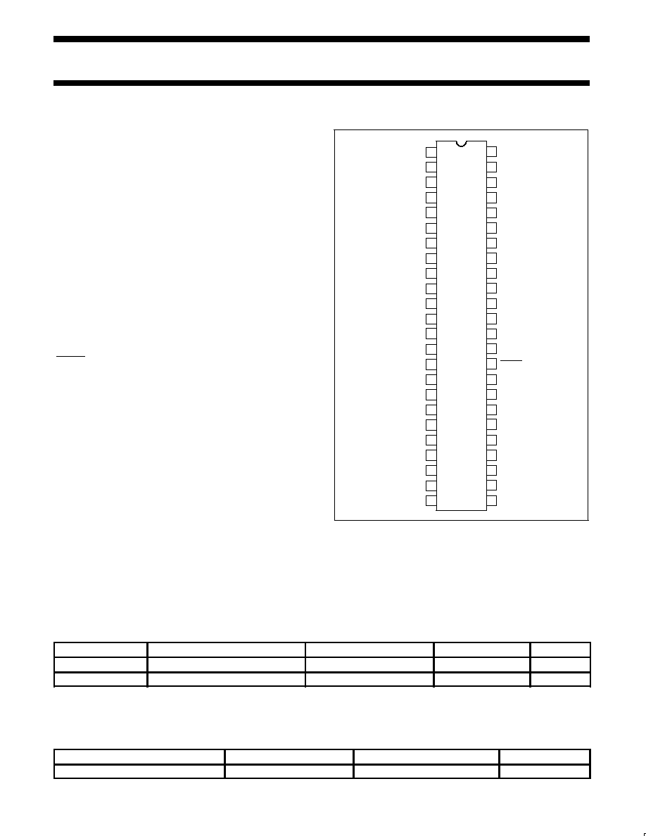
PIN CONFIGURATION
1
2
3
4
5
6
7
8
9
10
11
12
13
14
15
16
17
18
19
20
29
30
31
32
33
34
35
36
37
38
39
40
41
42
43
44
45
46
47
48
VDDQ
Q5
Q6
Q9
Q10
D12
D11
D10
D9
D8
RESET
VREF
GND
VCC
CLK+
CLK¡
D7
D6
D5
D4
D3
VCC
GND
D2
D1
21
22
23
24
25
26
27
28
VDDQ
Q14
D14
D13
GND
VCC
Q1
Q2
GND
Q3
Q4
GND
VDDQ
Q7
VDDQ
GND
Q8
VDDQ
GND
Q11
Q12
GND
Q13
SW00311
QUICK REFERENCE DATA
GND = 0 V; T
amb
= 25
░
C; t
r
=t
f
v
2.5 ns
SYMBOL
PARAMETER
CONDITIONS
TYPICAL
UNIT
t
PHL
/t
PLH
Propagation delay; CLK to Qn
C
L
= 30 pF; V
DDQ
= 2.5 V
2.4
ns
C
I
Input capacitance
V
CC
= 2.5 V
2.9
pF
NOTES:
1. C
PD
is used to determine the dynamic power dissipation (P
D
in
Á
W) P
D
= C
PD
V
CC
2
x f
i
)
(C
L
V
CC
2
f
o
) where:
f
i
= input frequency in MHz; C
L
= output load capacity in pF; f
o
= output frequency in MHz; V
CC
= supply voltage in V;
(C
L
V
CC
2
f
o
) = sum of the outputs.
ORDERING INFORMATION
PACKAGES
TEMPERATURE RANGE
ORDER CODE
DWG NUMBER
48-Pin Plastic TSSOP Type I
0
░
C to +70
░
C
SSTL16877 DGG
SOT362-1

Philips Semiconductors
Product specification
SSTL16877
14-bit SSTL_2 registered driver with
differential clock inputs
2000 Apr 20
3
PIN DESCRIPTION
PIN NUMBER
SYMBOL
NAME AND FUNCTION
34
RESET
LVCMOS asynchronous master
reset
(Active LOW)
48, 47, 44, 43,
42, 41, 40, 33,
32, 31, 30, 29,
26, 25
D1 ¡ D14
SSTL_2 data inputs
1, 2, 5, 6, 7, 10,
11, 14, 15, 18,
19, 20, 23, 24
Q1 ¡ Q14
SSTL_2 data outputs
35
VREF
SSTL_2 input reference level
3, 8, 13, 17, 22,
27, 36, 46
GND
Ground (0 V)
28, 37, 45
V
CC
Positive supply voltage
4, 9, 12, 16, 21
V
DDQ
Output supply voltage
38
39
CLK+
CLK¡
Differential clock inputs
FUNCTION TABLE
INPUTS
OUTPUT
RESET
CLK
CLK
D
Q
L
X
X
X
L
H
H
H
H
L
L
H
L or H
L or H
X
Q
0
H = High voltage level
L = High voltage level
= High-to-Low transition
= Low-to-High transition
X = Don't care
LOGIC DIAGRAM
SW00312
REGISTER
REGISTER
REGISTER
REGISTER
REGISTER
REGISTER
REGISTER
REGISTER
REGISTER
REGISTER
REGISTER
REGISTER
REGISTER
REGISTER
RESET
VREF
D1
D2
AD
D4
D5
D6
D7
D8
D9
D10
D11
D12
D13
D14
CLK+
CLK¡
Q1
Q2
Q3
Q4
Q5
Q6
Q7
Q8
Q9
Q10
Q11
Q12
Q13
Q14
ABSOLUTE MAXIMUM RATINGS
1, 2
SYMBOL
PARAMETER
CONDITION
LIMITS
UNIT
SYMBOL
PARAMETER
CONDITION
MIN
MAX
UNIT
V
CC
DC supply voltage
¡0.5
+4.6
V
I
IK
DC input diode current
V
I
< 0
¡50
mA
V
I
DC input voltage
3
¡0.5
V
DDQ
+ 0.5
V
I
OK
DC output diode current
V
O
< 0
¡50
mA
V
OUT
DC output voltage
3
Note 3
¡0.5
V
DDQ
+ 0.5
V
I
O
DC output current
V
O
= 0 to V
DDQ
▒
50
mA
I
OUT
Continuous current
4
V
CC
, V
DDQ
, or GND
▒
100
mA
T
STG
Storage temperature range
¡65
+150
░
C
NOTES:
1. Stresses beyond those listed may cause permanent damage to the device. These are stress ratings only and functional operation of the
device at these or any other conditions beyond those indicated under "recommended operating conditions" is not implied. Exposure to
absolute-maximum-rated conditions for extended periods may affect device reliability.
2. The performance capability of a high-performance integrated circuit in conjunction with its thermal environment can create junction
temperatures which are detrimental to reliability. The maximum junction temperature of this integrated circuit should not exceed 150
░
C.
3. The input and output voltage ratings may be exceeded if the input and output current ratings are observed.
4. The continuous current at V
CC
, V
DDQ
, or GND should not exceed
▒
100 mA.
Philips Semiconductors
Product specification
SSTL16877
14-bit SSTL_2 registered driver with
differential clock inputs
2000 Apr 20
4
RECOMMENDED OPERATING CONDITIONS
1
SYMBOL
PARAMETER
TEST CONDITIONS
MIN
TYP
MAX
UNIT
V
CC
Supply voltage
2.3
2.5
2.7
V
V
DDQ
Output supply voltage
2.3
2.5
2.7
V
V
REF
Reference voltage
(V
REF
= 0.5 x V
DDQ
)
1.15
1.25
1.35
V
V
TT
Termination voltage
V
REF
¡ 40 mV
V
REF
V
REF
+ 40 mV
V
V
I
Input voltage
0
V
CC
V
V
IH
AC HIGH-level input voltage
All inputs
V
REF
+ 350 mV
V
V
IL
AC LOW-level input voltage
All inputs
V
REF
¡ 350 mV
V
V
IH
DC HIGH-level input voltage
All inputs
V
REF
+ 180 mV
V
DDQ
+ 0.5 V
V
V
IL
DC LOW-level input voltage
All inputs
V
SS
¡ 0.5 V
V
REF
¡ 180 mV
V
I
OH
HIGH-level output current
¡20
mA
I
OL
LOW-level output current
20
mA
Tamb
Operating free-air temperature range
0
70
░
C
NOTE:
1. Unused control inputs must be held HIGH or LOW to prevent them from floating.
DC ELECTRICAL CHARACTERISTICS
Over recommended operating conditions. Voltages are referenced to GND (ground = 0 V).
LIMITS
SYMBOL
PARAMETER
TEST CONDITIONS
Temp = 0
░
C to +70
░
C
UNIT
MIN
TYP
2
MAX
V
IK
I/O supply voltage
V
CC
= 2.3 V; I
I
= ¡18 mA
¡1.2
V
CC
= 2.3 V to 2.7 V; I
OH
= ¡100
Á
A
V
CC
¡ 0.2
2.3
V
V
OH
HIGH level output voltage
V
CC
= 2.3 V; I
OH
= ¡8 mA
1.95
2.2
V
V
CC
= 2.3 V; I
OH
= ¡16 mA
1.95
2.1
V
CC
= 2.3 V to 2.7 V; I
OL
= ¡100
Á
A
0.002
0.2
V
OL
LOW level output voltage
V
CC
= 2.3 V; I
OL
= ¡8 mA
0.14
0.35
V
V
CC
= 2.3 V; I
OL
= ¡16 mA
0.30
0.35
V
CMR
CLK, CLK
Common mode range for reliable performance
0.97
1.53
V
V
PP
CLK, CLK
Minimum peak-to-peak input to ensure logic state
360
mV
Data inputs RESET
V
CC
= 2.7 V ; V
I
= 1.7 V or 0.8 V
V
= 1 15V or 1 35V
0.01
▒
5
Á
A
Data inputs, RESET
V
CC
= 2.7 V ; V
I
= 2.7 V or 0 V
V
REF
= 1.15V or 1.35V
0.01
▒
5
Á
A
I
I
CLK CLK
V
CC
= 2.7 V ; V
I
= 1.7 V or 0.8 V
V
= 1 15V or 1 35V
0.05
▒
5
Á
A
CLK, CLK
V
CC
= 2.7 V ; V
I
= 2.7 V or 0 V
V
REF
= 1.15V or 1.35V
0.05
▒
5
Á
A
V
REF
V
CC
= 2.7 V
V
REF
= 1.15V or 1.35V
0.05
▒
5
Á
A
I
CC
Quiescent supply current
CLK and CLK in opposite
V
CC
= 2.7 V ; V
I
= 1.7 V or 0.8 V
12
25
mA
I
CC
CLK and CLK in o
osite
state
1
V
CC
= 2.7 V ; V
I
= 2.7 V or 0 V
10
25
mA
NOTES:
1. When CLK and CLK are HIGH, typical I
CC
= 25 mA.
2. All typical values are at V
CC
= 3.3 V and T
amb
= 25
░
C (unless otherwise specified).

Philips Semiconductors
Product specification
SSTL16877
14-bit SSTL_2 registered driver with
differential clock inputs
2000 Apr 20
5
TIMING REQUIREMENTS
Over recommended operating conditions; T
amb
= 0
_
C to +70
_
C (unless otherwise noted) (see Figure 1)
LIMITS
SYMBOL
PARAMETER
TEST CONDITIONS
V
CC
= 2.5 V
▒
0.2 V
UNIT
MIN
MAX
f
clock
Clock frequency
200
MHz
t
w
Pulse duration, CLK, CLK HIGH or LOW
1.0
ns
t
Setup time
Data before CLK
, CLK
0.2
ns
t
su
Setup time
RESET HIGH before CLK
, CLK
0.8
ns
t
h
Hold time
1.2
ns
SWITCHING CHARACTERISTICS
Over recommended operating conditions; T
amb
= 0
_
C to +70
_
C; V
DDQ
= 2.3 ¡ 2.7 V and V
DDQ
does not exceed V
CC.
Class I, V
REF
= V
TT
= V
DDQ
x 0.5 and C
L
= 10 pF (unless otherwise noted) (see Figure 1)
LIMITS
SYMBOL
FROM
(INPUT)
TO
(OUTPUT)
V
CC
= 2.5 V
▒
0.2 V
UNIT
(INPUT)
(OUTPUT)
MIN
MAX
f
max
Maximum clock frequency
200
MHz
t
PLH
/t
PHL
CLK and CLK
Q
1.0
3.5
ns
t
PHL
RESET
Q
2.0
4.0
ns
184/200-pin DDR SDRAM DIMM
SDRAM
SDRAM
SDRAM
SDRAM
SDRAM
SDRAM
SDRAM
SDRAM
SDRAM
The PLL clock distribution device and SSTL registered drivers reduce
signal loads on the memory controller and prevent timing delays and
waveform distortions that would cause unreliable operation
SW00502
CBT3867 (9)
CBT
CBT
CBT
CBT
CBT
CBT
CBT
CBT
CBT
SDRAM
SDRAM
SDRAM
SDRAM
SDRAM
SDRAM
SDRAM
SDRAM
SDRAM
SSTL16877
PCK877
SSTL16877
BACK SIDE
FRONT SIDE

Philips Semiconductors
Product specification
SSTL16877
14-bit SSTL_2 registered driver with
differential clock inputs
2000 Apr 20
6
PARAMETER MEASUREMENT INFORMATION
AC WAVEFORMS
V
OL
t
PLH
t
PHL
OUTPUT
V
REF
V
REF
V
REF
V
IH
V
IL
CLK
V
OH
V
REF
SW00338
Waveform 1. Propagation delay times inverting and
non-inverting outputs
V
REF
V
REF
V
IH
V
IL
OUTPUT
t
PHL
SW00402
V
OH
V
OL
RESET
Waveform 2. Propagation delay RESET to output.
V
REF
V
REF
V
IH
V
IL
INPUT
SW00339
t
W
Waveform 3. Pulse duration
V
REF
V
IH
V
IL
TIMING INPUT
SW00340
V
REF
V
REF
V
IL
DATA INPUT
t
h
t
su
V
IH
Waveform 4. Setup and hold times
TEST CIRCUIT
V
TT
TEST
POINT
25
C
L
= 10pF or 30pF
25
= SSTL_2 Class II
50
= SSTL_2 Class I
NOTES:
C
L
includes probe and jig capacitance
All input pulses are supplied by generators having the following characteristics:
PRR
10MHz, Z
O
= 50
, t
r
1.25ns/V, t
f
1.25ns/V.
The outputs are measured one at a time with one transition per measurement.
V
TT
= V
REF
= V
DDQ
x 0.5
SW00337
Figure 1. Load circuitry
50pF
500
SW00336
Figure 2.
SW00335
50pF
Figure 3.

Philips Semiconductors
Product specification
SSTL16877
14-bit SSTL_2 registered driver with
differential clock inputs
2000 Apr 20
7
TSSOP48:
plastic thin shrink small outline package; 48 leads; body width 6.1 mm
SOT362-1

Philips Semiconductors
Product specification
SSTL16877
14-bit SSTL_2 registered driver with
differential clock inputs
2000 Apr 20
8
Definitions
Short-form specification -- The data in a short-form specification is extracted from a full data sheet with the same type number and title. For
detailed information see the relevant data sheet or data handbook.
Limiting values definition -- Limiting values given are in accordance with the Absolute Maximum Rating System (IEC 134). Stress above one
or more of the limiting values may cause permanent damage to the device. These are stress ratings only and operation of the device at these or
at any other conditions above those given in the Characteristics sections of the specification is not implied. Exposure to limiting values for extended
periods may affect device reliability.
Application information -- Applications that are described herein for any of these products are for illustrative purposes only. Philips
Semiconductors make no representation or warranty that such applications will be suitable for the specified use without further testing or
modification.
Disclaimers
Life support -- These products are not designed for use in life support appliances, devices or systems where malfunction of these products can
reasonably be expected to result in personal injury. Philips Semiconductors customers using or selling these products for use in such applications
do so at their own risk and agree to fully indemnify Philips Semiconductors for any damages resulting from such application.
Right to make changes -- Philips Semiconductors reserves the right to make changes, without notice, in the products, including circuits, standard
cells, and/or software, described or contained herein in order to improve design and/or performance. Philips Semiconductors assumes no
responsibility or liability for the use of any of these products, conveys no license or title under any patent, copyright, or mask work right to these
products, and makes no representations or warranties that these products are free from patent, copyright, or mask work right infringement, unless
otherwise specified.
Philips Semiconductors
811 East Arques Avenue
P.O. Box 3409
Sunnyvale, California 94088¡3409
Telephone 800-234-7381
®
Copyright Philips Electronics North America Corporation 2000
All rights reserved. Printed in U.S.A.
Date of release: 04-00
Document order number:
9397 750 07086
Philips
Semiconductors
Data sheet
status
Objective
specification
Preliminary
specification
Product
specification
Product
status
Development
Qualification
Production
Definition
[1]
This data sheet contains the design target or goal specifications for product development.
Specification may change in any manner without notice.
This data sheet contains preliminary data, and supplementary data will be published at a later date.
Philips Semiconductors reserves the right to make changes at any time without notice in order to
improve design and supply the best possible product.
This data sheet contains final specifications. Philips Semiconductors reserves the right to make
changes at any time without notice in order to improve design and supply the best possible product.
Data sheet status
[1]
Please consult the most recently issued datasheet before initiating or completing a design.