
DATA SHEET
Product specification
Supersedes data of 1999 May 17
File under Integrated Circuits, IC18
1999 Jun 04
INTEGRATED CIRCUITS
SAA1575HL
Global Positioning System (GPS)
baseband processor

1999 Jun 04
2
Philips Semiconductors
Product specification
Global Positioning System (GPS)
baseband processor
SAA1575HL
CONTENTS
1
FEATURES
2
GENERAL DESCRIPTION
3
QUICK REFERENCE DATA
4
ORDERING INFORMATION
5
BLOCK DIAGRAM
6
PINNING
7
FUNCTIONAL DESCRIPTION
7.1
Overview
7.2
The 80C51XA processor
7.3
The GPS correlators
7.4
Memory organization
7.4.1
Data memory space
7.4.2
Code memory space
7.5
CPU peripheral features
7.5.1
Timers/counters
7.5.2
Watchdog timer
7.5.3
UARTs
7.5.4
RF IC programming port
7.5.5
General purpose I/O
7.6
The real-time clock
7.7
The external bus
7.7.1
Program memory chip select
7.7.2
Data memory chip select
7.7.3
Read strobe
7.7.4
Write LOW byte strobe
7.7.5
Write HIGH byte strobe
7.8
Backup supplies and reset
7.8.1
Supply domains
7.8.2
Power-down design strategy
7.8.3
System reset control
7.8.4
Power saving modes
7.9
Clock signals and oscillators
7.9.1
System clock (XTAL1)
7.9.2
RTC clock (XTAL3)
7.9.3
Reference clock (RCLK)
8
LIMITING VALUES
9
THERMAL CHARACTERISTICS
10
DC CHARACTERISTICS
11
AC CHARACTERISTICS
12
DEFAULT APPLICATION AND
DEMONSTRATION BOARD
13
PACKAGE OUTLINE
14
SOLDERING
14.1
Introduction to soldering surface mount
packages
14.2
Reflow soldering
14.3
Wave soldering
14.4
Manual soldering
14.5
Suitability of surface mount IC packages for
wave and reflow soldering methods
15
DEFINITIONS
16
LIFE SUPPORT APPLICATIONS

1999 Jun 04
3
Philips Semiconductors
Product specification
Global Positioning System (GPS)
baseband processor
SAA1575HL
1
FEATURES
·
Single-chip GPS baseband solution with built-in 16-bit
microcontroller
·
All digital, 0.5 micron CMOS technology
·
Single power supply with full 3 V operation
·
Separate I/O power supply pins for operation with
3 or 5 V external devices
·
Up to 30 MHz system clock from on-chip crystal
oscillator or external clock input
·
2 kbytes words internal data memory for fast execution
·
External bus for up to 512 kbytes words data memory
and 512 kbytes words program memory
·
Programmable external bus timing to match external
memory speed
·
Chip selection outputs to reduce glue logic requirements
·
Reset controller for power-down detection and servicing
·
8 GPS channel correlators driven by firmware for
flexible GPS correlation algorithms
·
1 second pulse output of GPS time
·
2-bit digital IF GPS signal input synchronized to external
sample clock
·
2 fully duplex UARTs for communication with host
system processor and other devices
·
Real-time clock with 32.768 kHz crystal and supply for
low power timekeeping
·
Watchdog timer
·
Power-down modes under firmware control
·
100-pin LQFP package
·
50 mA supply current (typ.) when 8 GPS channels in
track (approximate).
2
GENERAL DESCRIPTION
The SAA1575HL is an integrated circuit which implements
a complete baseband function for Global Positioning
System (GPS) receivers. It combines a 16-bit Philips
80C51XA microcontroller, 8 GPS channel correlators and
related peripherals in a single IC. Users can implement a
complete GPS receiver using only the SAA1575HL, the
UAA1570HL front-end Philips IC (or similar), external
memory and a few discrete components.
The IC is aimed at low cost applications. A low power
solution was also used where possible, although this was
of secondary importance to cost. The core of the
SAA1575HL operates at 3 V.
However, for compatibility with current automotive
applications, the periphery is supplied from separate pins
and can be operated between 3 and 5 V, as required.
The function of the SAA1575HL is to read the 1 or 2-bit
sampled IF bitstream from a front-end IC and, under
control of firmware on an external ROM, calculate the full
GPS solution. The results are communicated to a host in
National Maritime Electronics Association (NMEA) format
via a standard serial port. A second serial port can be used
to provide differential GPS information to the processor for
more advance applications. In addition, various other
functions are integrated onto the IC such as a real-time
GPS clock, a power-down/reset controller, timer/counters
and a watchdog timer.
To summarise, the SAA1575HL has the following
functional units:
·
16-bit 80C51XA microcontroller core
·
2 kbytes words on-chip SRAM (16-bit words)
·
8 GPS channel correlators
·
2 UARTs
·
8 general purpose I/O lines
·
3 timer/counters
·
1 real-time clock
·
1 watchdog timer
·
1 power-down/reset controller.
The structure is based on a 16-bit microcontroller core
operating on all other units as memory mapped
peripherals and registers. A 16-bit data bus and a 19-bit
address bus are extended to external pins so that external
data and program memory can be accessed. On-chip
decoder circuits eliminate the need for external glue logic
for external memory access.
Each of the 8 GPS channel correlators includes a carrier
Numerically Controlled Oscillator (NCO), PN code
generator, phase rotator and low-pass filter. They
correlate the local PN sequence with the digitized input
GPS signal and generate the filtered correlation result for
the microcontroller. The firmware provided then generates
a navigation solution and provides standard GPS data
outputs to the user.
1999 Jun 04
4
Philips Semiconductors
Product specification
Global Positioning System (GPS)
baseband processor
SAA1575HL
The GPS firmware is located in off-chip program memory. It processes the GPS signals from up to 8 satellites and
generates GPS information that can be output to the host processor through one of the two serial ports. Much of
hardware configuration of the SAA1575HL can be controlled by the firmware and so details such as the external bus
timing may change between firmware revisions. For the purpose of this document, the standard Philips firmware has
been assumed (release HD00).
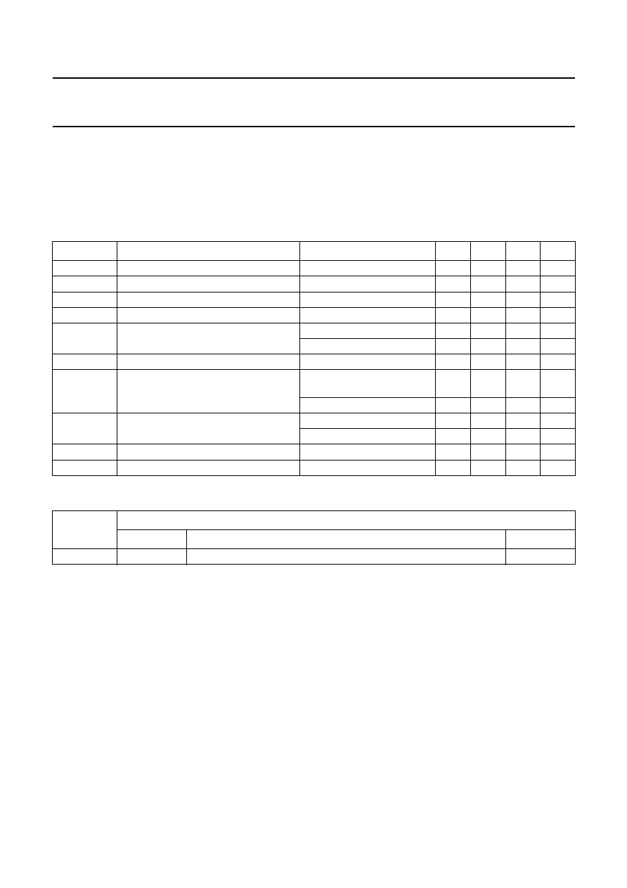
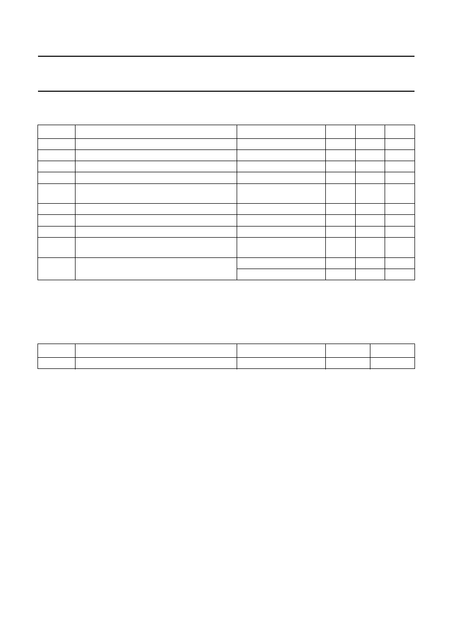
3
QUICK REFERENCE DATA
4
ORDERING INFORMATION
SYMBOL
PARAMETER
CONDITIONS
MIN.
TYP.
MAX.
UNIT
V
CC(core)
core supply voltage
2.7
3.3
3.6
V
V
CC(P)
peripheral supply voltage
2.7
5.0
5.5
V
V
CC(R)
real-time clock core supply voltage
2.4
3.3
3.6
V
V
CC(B)
backup peripheral supply voltage
2.7
5.0
5.5
V
I
CC(core)
core supply current
normal mode
-
35
-
mA
sleep mode
-
15
-
mA
I
CC(R)
real-time clock core supply current
f
RTC
= 32.768 kHz
-
10
30
µ
A
I
CC(B)
backup peripheral supply current
normal mode; dependent on
load
-
5
-
mA
sleep mode
-
1
-
µ
A
I
CC(P)
peripheral supply current
normal mode
-
20
-
mA
sleep mode
-
-
1
mA
f
osc
oscillator frequency
26
30
32
MHz
T
amb
ambient temperature
-
40
+25
+85
°
C
TYPE
NUMBER
PACKAGE
NAME
DESCRIPTION
VERSION
SAA1575HL
LQFP100
plastic low profile quad flat package; 100 leads; body 14
×
14
×
1.4 mm
SOT407-1
1999 Jun 04
5
Philips Semiconductors
Product specification
Global Positioning System (GPS)
baseband processor
SAA1575HL
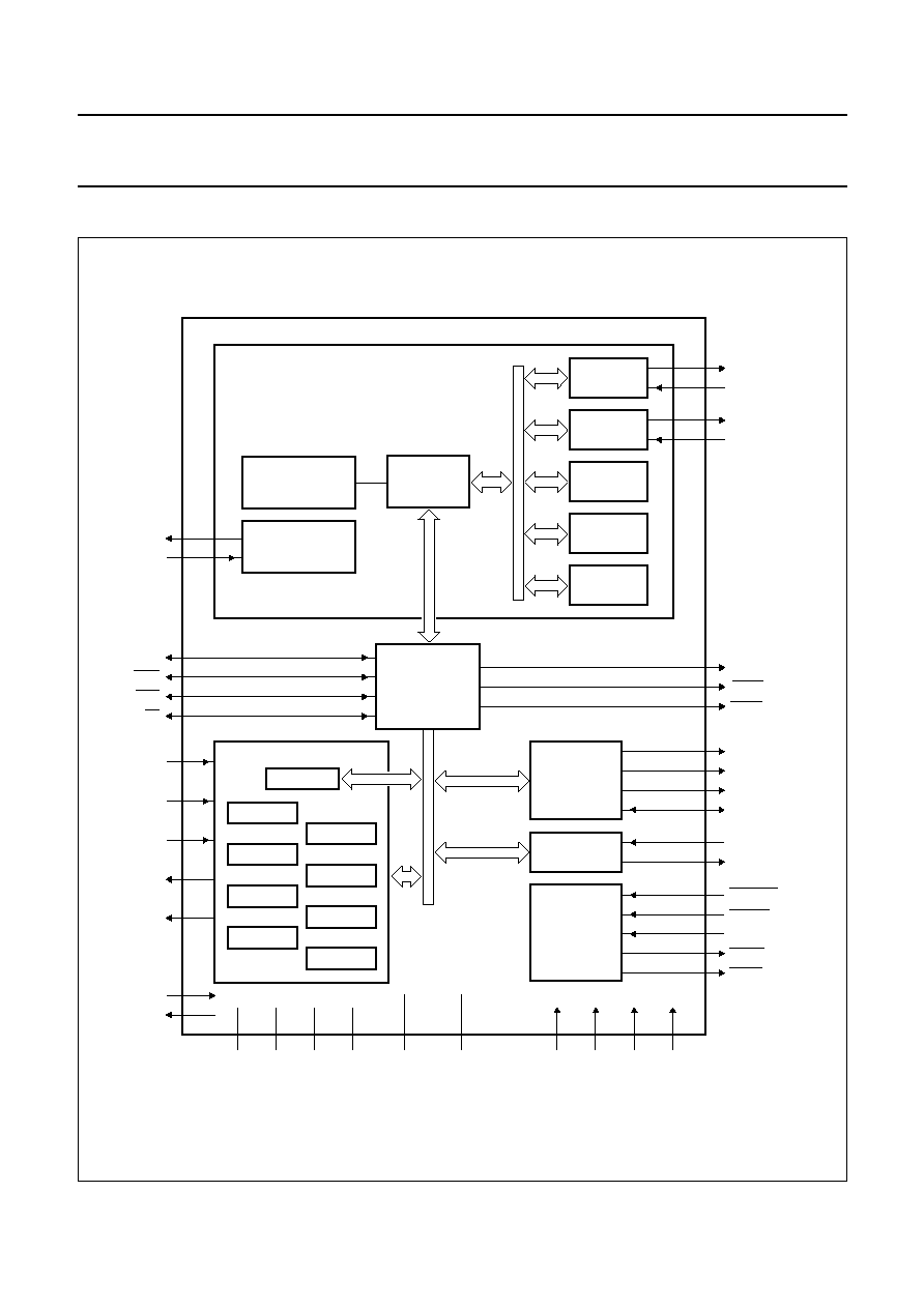
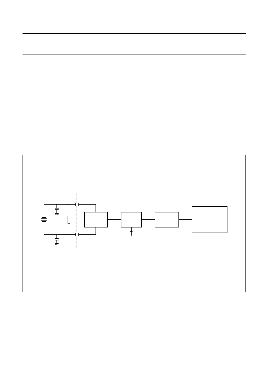
5
BLOCK DIAGRAM
Fig.1 Block diagram.
MHB460
handbook, full pagewidth
UART 0
UART 1
TIMER 0, 1
80C51XA
CORE
SAA1575HL
80C51XA PROCESSOR MODULE
EXTERNAL BUS
INTERFACE
TIMER 2
WATCHDOG
TIMER
ADDRESS
AND
DATA
STATIC RAM
(2 kbytes WORDS)
SYSTEM CLOCK
GENERATOR
14
48, 49, 53 to 59, 62 to 64, 67 to 70
15
2
100
93
92
98
99
8, 9
97
72
80
12, 30,
66
16, 25,
37, 51,
61, 86
13, 17, 26, 31,
38, 50, 60, 65,
71, 79, 85
4
3
42
44
1
45
46
47
83
81
84
82
CONTROL
REGISTERS
CORRELATORS
89
90
91
5 to 7, 87, 88,
94 to 96
REAL-TIME
CLOCK
CHANNEL 7
CHANNEL 6
CHANNEL 5
CHANNEL 4
CHANNEL 3
CHANNEL 2
CHANNEL 1
CHANNEL 0
CONTROL
76
75
RESET
CONTROLLER
74
78
52
43
77
10, 11, 18 to 24, 27 to 29, 32 to 36, 39, 40
41
73
SCLK
T1S
TEST2
TEST1
RCLK
n.c.
GPIO7 to GPIO0
A19 to A1
IF1
IF2
PMCS
TP2
RSTIME
TP1
D15 to D0
VSS
VCC(P)
VCC(R) VCC(B)
WRH
WRL
RD
XTAL1
XTAL2
TP3
TP4
VCC(core)
PWRM
PWRB
XTAL3
RXD0
TXD0
RXD1
TXD1
RFLE
RFCLK
RFDAT
PWRDN
XTAL4
PWRFAIL
DMCS

1999 Jun 04
6
Philips Semiconductors
Product specification
Global Positioning System (GPS)
baseband processor
SAA1575HL
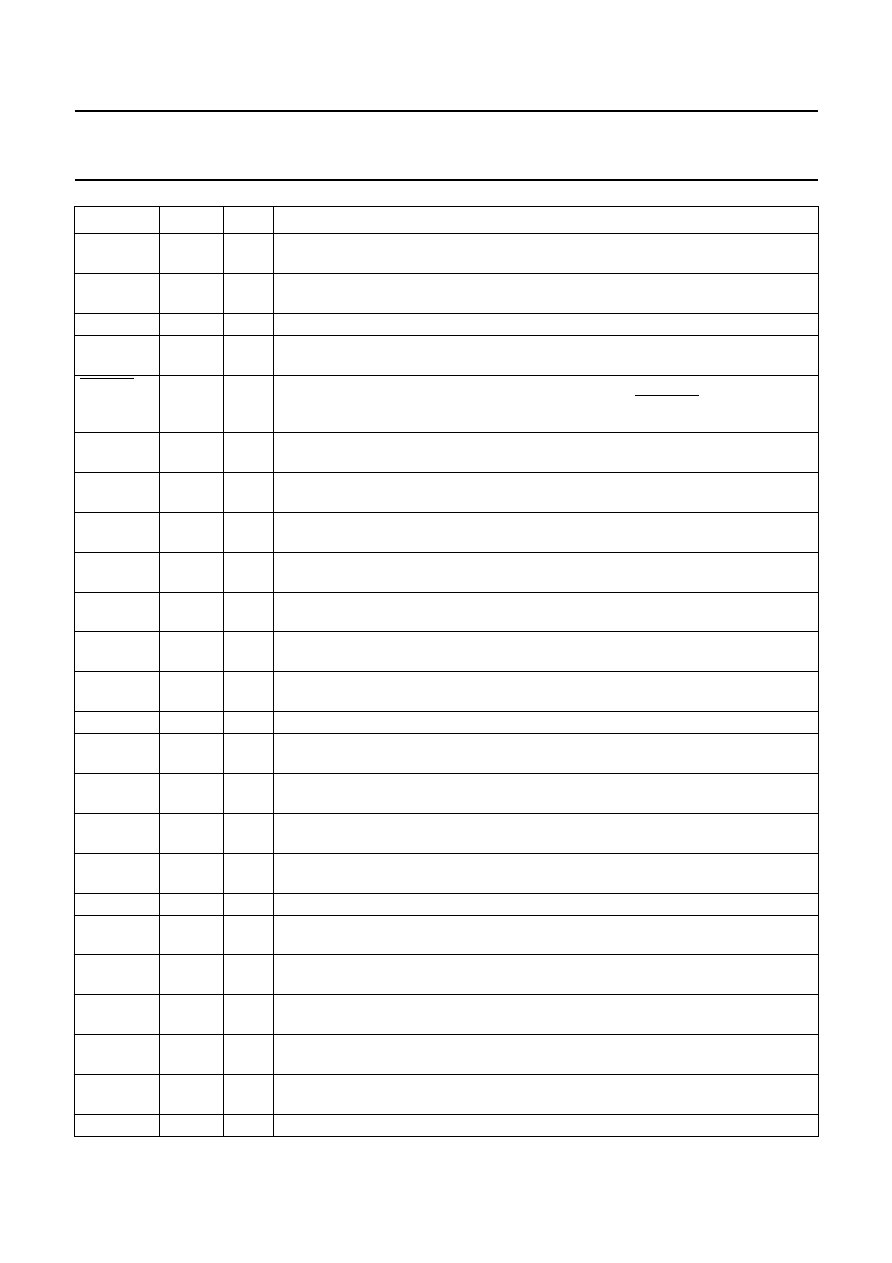
6
PINNING
SYMBOL
PIN
I/O
DESCRIPTION
SCLK
1
O
Sample clock: sample clock generated internally by dividing down the RCLK
(reference clock) input. This output is provided for use by the front-end IC.
T1S
2
O
GPS time pulse: a 1 pulse per second output whose rising or falling edge (firmware
controlled) is synchronized to GPS time when the receiver is tracking a GPS signal.
The pulse length is approximately 1 ms.
TP3
3
I
Test pin: tie HIGH
TP4
4
I
Test pin: tie HIGH
GPIO5
5
I/O
GPIO bit 5: standard general purpose I/O mapped into the segment 15 of the address
space. The top 4 bits can be used as the XA external timer control access pins
(T0, T1, T2 and T2EX).
GPIO6
6
I/O
GPIO bit 6: standard general purpose I/O mapped into the segment 15 of the address
space. The top 4 bits can be used as the XA external timer control access pins
(T0, T1, T2 and T2EX).
GPIO7
7
I/O
GPIO bit 7: standard general purpose I/O mapped into the segment 15 of the address
space. The top 4 bits can be used as the XA external timer control access pins
(T0, T1, T2 and T2EX).
n.c.
8
O
Not connected: do not connect
n.c.
9
O
Not connected: do not connect
A19
10
O
External memory address bus bit 19: 19-bit address bus; used to address external
RAM and program memory
A18
11
O
External memory address bus bit 18: 19-bit address bus; used to address external
RAM and program memory
V
CC(core)
12
-
Main core power supply: 2.7 to 3.6 V only; main supply for the core in normal
operation
V
SS
13
-
Ground: 0 V reference
XTAL1
14
I
Crystal 1: input to the inverting amplifier; used in the system oscillator circuit and
input to the internal clock generator circuits
XTAL2
15
O
Crystal 2: output from the system oscillator amplifier
V
CC(P)
16
-
Main I/O power supply: 2.7 to 5.5 V operating range; main supply for the periphery
in normal operation
V
SS
17
-
Ground: 0 V reference
A17
18
O
External memory address bus bit 17: 19-bit address bus; used to address external
RAM and program memory
A16
19
O
External memory address bus bit 16: 19-bit address bus; used to address external
RAM and program memory
A15
20
O
External memory address bus bit 15: 19-bit address bus; used to address external
RAM and program memory
A14
21
O
External memory address bus bit 14: 19-bit address bus; used to address external
RAM and program memory
A13
22
O
External memory address bus bit 13: 19-bit address bus; used to address external
RAM and program memory
A12
23
O
External memory address bus bit 12: 19-bit address bus; used to address external
RAM and program memory

1999 Jun 04
7
Philips Semiconductors
Product specification
Global Positioning System (GPS)
baseband processor
SAA1575HL
A11
24
O
External memory address bus bit 11: 19-bit address bus; used to address external
RAM and program memory
V
CC(P)
25
-
Main I/O power supply: 2.7 to 5.5 V operating range; main supply for the periphery
in normal operation
V
SS
26
-
Ground: 0 V reference
A10
27
O
External memory address bus bit 10: 19-bit address bus; used to address external
RAM and program memory
A9
28
O
External memory address bus bit 9: 19-bit address bus; used to address external
RAM and program memory
A8
29
O
External memory address bus bit 8: 19-bit address bus; used to address external
RAM and program memory
V
CC(core)
30
-
Main core power supply: 2.7 to 3.6 V only; main supply for the core in normal
operation
V
SS
31
-
Ground: 0 V reference
A7
32
O
External memory address bus bit 7: 19-bit address bus; used to address external
RAM and program memory
A6
33
O
External memory address bus bit 6: 19-bit address bus; used to address external
RAM and program memory
A5
34
O
External memory address bus bit 5: 19-bit address bus; used to address external
RAM and program memory
A4
35
O
External memory address bus bit 4: 19-bit address bus; used to address external
RAM and program memory
A3
36
O
External memory address bus bit 3: 19-bit address bus; used to address external
RAM and program memory
V
CC(P)
37
-
Main I/O power supply: 2.7 to 5.5 V operating range; main supply for the periphery
in normal operation
V
SS
38
-
Ground: 0 V reference
A2
39
O
External memory address bus bit 2: 19-bit address bus; used to address external
RAM and program memory
A1
40
O
External memory address bus bit 1: 19-bit address bus; used to address external
RAM and program memory
PMCS
41
O
External program memory select: external program memory read strobe
TP2
42
I
Test pin: tie LOW
RSTIME
43
I
Reset timer control: this controls the on-chip reset timer. If this is HIGH, reset will be
de-asserted approximately 10 ms after both PWRDN and PWRFAIL go HIGH. If this
is LOW, reset will be de-asserted approximately 10
µ
s after both
PWRDN and PWRFAIL go HIGH.
TP1
44
I
Test pin: tie LOW
WRH
45
I/O
Write MSB: write strobe for external data memory; asserted for both MSB and word
write operations; input mode only used for test purposes
WRL
46
I/O
Write LSB: write strobe for external data memory; asserted for both LSB and word
write operations; input mode only used for test purposes
RD
47
I/O
External data read: read strobe for external data memory; input mode only used for
test purposes
SYMBOL
PIN
I/O
DESCRIPTION
1999 Jun 04
8
Philips Semiconductors
Product specification
Global Positioning System (GPS)
baseband processor
SAA1575HL
D15
48
I/O
External memory data bus: 16-bit data bus; used to connect to external RAM and
program memory
D14
49
I/O
External memory data bus bit 14: 16-bit data bus; used to connect to external RAM
and program memory
V
SS
50
-
Ground: 0 V reference
V
CC(P)
51
-
Main I/O power supply: 2.7 to 5.5 V operating range; main supply for the periphery
in normal operation
PWRDN
52
I
Power-down indicator: a LOW on this pin asserts an XA interrupt intended for use
as a power fail interrupt. Once reset is asserted, either by PWRFAIL or the firmware, it
will remain asserted until a set time after this pin goes HIGH.
D13
53
I/O
External memory data bus bit 13: 16-bit data bus; used to connect to external RAM
and program memory
D12
54
I/O
External memory data bus bit 12: 16-bit data bus; used to connect to external RAM
and program memory
D11
55
I/O
External memory data bus bit 11: 16-bit data bus; used to connect to external RAM
and program memory
D10
56
I/O
External memory data bus bit 10: 16-bit data bus; used to connect to external RAM
and program memory
D9
57
I/O
External memory data bus bit 9: 16-bit data bus; used to connect to external RAM
and program memory
D8
58
I/O
External memory data bus bit 8: 16-bit data bus; used to connect to external RAM
and program memory
D7
59
I/O
External memory data bus bit 7: 16-bit data bus; used to connect to external RAM
and program memory
V
SS
60
-
Ground: 0 V reference
V
CC(P)
61
-
Main I/O power supply: 2.7 to 5.5 V operating range; main supply for the periphery
in normal operation
D6
62
I/O
External memory data bus bit 6: 16-bit data bus; used to connect to external RAM
and program memory
D5
63
I/O
External memory data bus bit 5: 16-bit data bus; used to connect to external RAM
and program memory
D4
64
I/O
External memory data bus bit 4: 16-bit data bus; used to connect to external RAM
and program memory
V
SS
65
-
Ground: 0 V reference
V
CC(core)
66
-
Main core power supply: 2.7 to 3.6 V only; main supply for the core in normal
operation
D3
67
I/O
External memory data bus bit 3: 16-bit data bus; used to connect to external RAM
and program memory
D2
68
I/O
External memory data bus bit 2: 16-bit data bus; used to connect to external RAM
and program memory
D1
69
I/O
External memory data bus bit 1: 16-bit data bus; used to connect to external RAM
and program memory
D0
70
I/O
External memory data bus bit 0: 16-bit data bus; used to connect to external RAM
and program memory
V
SS
71
-
Ground: 0 V reference
SYMBOL
PIN
I/O
DESCRIPTION

1999 Jun 04
9
Philips Semiconductors
Product specification
Global Positioning System (GPS)
baseband processor
SAA1575HL
V
CC(R)
72
-
Backup core power supply: 2.4 to 3.6 V only. Separate from the core supply to allow
a low capacity battery to be used to maintain the Real-Time Clock (RTC) function.
This should be powered from the main supply during normal operation and switched
to battery backup when the main supply fails.
DMCS
73
O
External data memory select: external RAM select pin, active LOW when the
external data memory space is addressed. This output is driven from V
CC(R)
and
V
CC(B)
supplies to ensure that the external RAM is not enabled during power-down.
PWRFAIL
74
I
Power fail indicator: a LOW on this pin forces the embedded microcontroller into
reset. Reset will not be de-asserted until a set time after both PWRDN and PWRFAIL
go HIGH. For correct start-up, this pin should be LOW on power-up.
XTAL4
75
O
Crystal 4: output from the RTC oscillator amplifier; this pin is only 3 V tolerant
XTAL3
76
I
Crystal 3: input to inverting amplifier used in the RTC oscillator circuits (32.768 kHz);
this pin is only 3 V tolerant
PWRB
77
O
Backup supply select: this output is intended to drive an external FET used to switch
the battery backup supply(s). It is active LOW and is controlled directly by the
PWRFAIL.
PWRM
78
O
Main supply select: this output is intended to drive an external FET used to switch
the main supply(s). It is active LOW and is controlled directly by PWRFAIL.
V
SS
79
-
Ground: 0 V reference
V
CC(B)
80
-
Backup I/O power supply: 2.4 to 5.5 V only. Supply for the RAM select, power fail
and power switching I/O pads only allowing these functions to be powered when the
main power supply fails. This should be powered from the main supply during normal
operation and switched to battery backup when the main supply fails.
TXD1
81
O
Transmitter output 1: transmit channel for serial port 1 (UART1) of the embedded
processor
RXD1
82
I
Receiver input 1: receive channel for serial port 1 (UART1) of the embedded
processor. It is intended that this serial port is dedicated to differential GPS
information (dependent on firmware).
TXD0
83
O
Transmitter output 0: transmit channel for serial port 0 (UART0) of the embedded
processor.
RXD0
84
I
Receiver input 0: receive channel for serial port 0 (UART0) of the embedded
processor. It is intended that this serial port is dedicated to the NMEA data stream
(dependent on firmware).
V
SS
85
-
Ground: 0 V reference
V
CC(P)
86
-
Main I/O power supply: 2.7 to 5.5 V operating range; main supply for the periphery
in normal operation
GPIO4
87
I/O
GPIO bit 4: standard general purpose I/O mapped into the segment 15 of the address
space. The top 4 bits can be used as the XA external timer control access pins
(T0, T1, T2 and T2EX).
GPIO3
88
I/O
GPIO bit 3: standard general purpose I/O mapped into the segment 15 of the address
space. The top 4 bits can be used as the XA external timer control access pins
(T0, T1, T2 and T2EX).
RFDAT
89
O
RFIC set-up data: serial data output used to set up the UAA1570HL front-end IC.
RFCLK
90
O
RFIC set-up data: clock output for the serial data output used to set up the
UAA1570HL front-end IC. The state of the RFDAT and RFLE lines is latched into the
front-end IC on the rising edge.
SYMBOL
PIN
I/O
DESCRIPTION

1999 Jun 04
10
Philips Semiconductors
Product specification
Global Positioning System (GPS)
baseband processor
SAA1575HL
RFLE
91
O
RFIC setup latch: output used to latch the RFIC set-up into the active UAA1570HL
control registers
IF2
92
I
MSB IF input: MSB of the 2-bit GPS digital IF signal input. Clocked in on the rising
edge of SCLK. If only a 1-bit IF input is available this input should be held HIGH.
IF1
93
I
LSB IF input: LSB of the 2-bit GPS digital IF signal input. Clocked in on the rising
edge of SCLK.
GPIO2
94
I/O
GPIO bit 2: standard general purpose I/O mapped into the segment 15 of the address
space. The top 4 bits can be used as the XA external timer control access pins
(T0, T1, T2 and T2EX).
GPIO1
95
I/O
GPIO bit 1: standard general purpose I/O mapped into the segment 15 of the address
space. The top 4 bits can be used as the XA external timer control access pins
(T0, T1, T2 and T2EX).
GPIO0
96
I/O
GPIO bit 0: standard general purpose I/O mapped into the segment 15 of the address
space. The top 4 bits can be used as the XA external timer control access pins
(T0, T1, T2 and T2EX).
n.c.
97
O
Not connected: do not connect
RCLK
98
I
Reference clock: input from the TXCO reference. Not used internally. This is divided
under firmware control to produce the sample clock, SCLK, used to gate the IF inputs.
TEST1
99
I
Test pin: connect to pin 100
TEST2
100
O
Test pin: connect to pin 99
SYMBOL
PIN
I/O
DESCRIPTION
1999 Jun 04
11
Philips Semiconductors
Product specification
Global Positioning System (GPS)
baseband processor
SAA1575HL
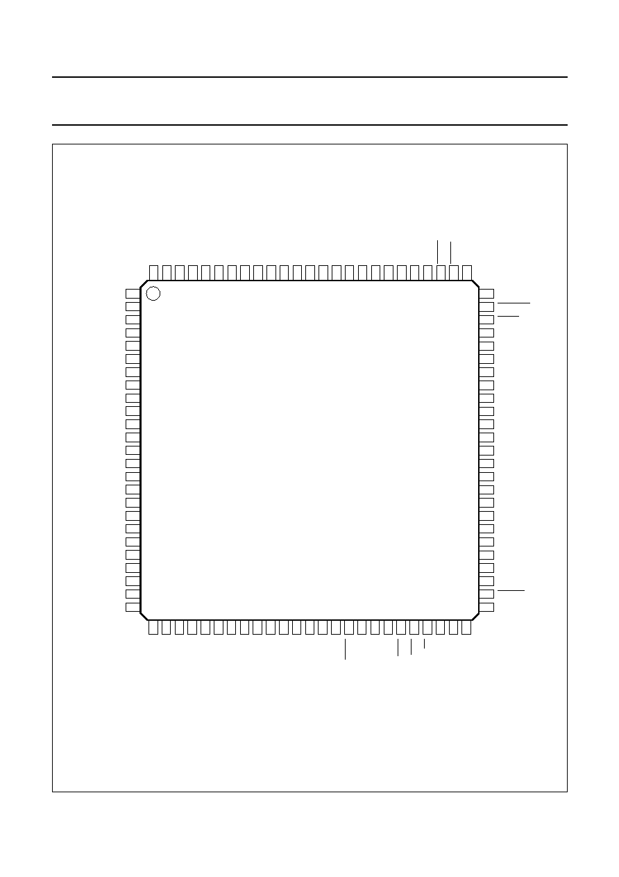
Fig.2 Pin configuration.
handbook, full pagewidth
75
74
73
72
71
70
69
68
67
66
65
64
63
62
61
60
59
58
57
56
55
54
53
52
51
80
79
78
77
76
V
CC(B)
V
SS
PWRM
PWRB
XTAL3
XTAL4
PWRFAIL
DMCS
VCC(R)
VSS
D0
D1
D2
D3
VCC(core)
VSS
D4
D5
D6
VCC(P)
VSS
D7
D8
D9
D10
D11
D12
D13
PWRDN
VCC(P)
SCLK
T1S
TP3
TP4
GPIO7
GPIO6
GPIO5
n.c.
n.c.
A19
A18
VCC(core)
VSS
XTAL1
XTAL2
VCC(P)
VSS
A17
A16
A15
A14
A13
A12
A11
VCC(P)
TEST2
TEST1
RCLK
n.c.
GPIO0
GPIO1
GPIO2
IF1
IF2
RFLE
RFCLK
RFDAT
GPIO3
GPIO4
V
CC(P)
V
SS
RXD0
TXD0
RXD1
TXD1
V
SS
A7
A6
A5
A4
A3
V
CC(P)
V
SS
A2
A1
PMCS
TP2
RSTIME
TP1
WRH
WRL
RD
D15
D14
V
SS
V
SS
A10
A9
A8
V
CC(core)
30
29
28
27
26
25
24
23
22
21
20
19
18
17
16
15
14
13
12
11
10
9
8
7
6
5
4
3
2
1
100
99
98
97
96
95
94
93
92
91
90
89
88
87
86
85
84
83
82
81
31
32
33
34
35
36
37
38
39
40
41
42
43
44
45
46
47
48
49
50
SAA1575HL
MHB461

1999 Jun 04
12
Philips Semiconductors
Product specification
Global Positioning System (GPS)
baseband processor
SAA1575HL
7
FUNCTIONAL DESCRIPTION
7.1
Overview
The function of the SAA1575HL is to accept any IF data
(1 or 2-bit) from a front-end RF IC (such as the
UAA1570HL) and provide a serial NMEA compatible GPS
position and time output. The IF input is sampled
synchronously with the front-end reference clock, SCLK.
Data is decoded from the IF input stream by one of eight
parallel correlators which allow up to eight satellites to be
tracked at one time. The acquisition, allocation and
tracking of the satellites is performed under firmware
control by the on-chip processor.
In addition to the SAA1575HL and an appropriate
front-end IC (such as the UAA1570HL), the only external
components required to complete a functional GPS
receiver are some RAM, the firmware ROM and some
discrete devices to control the power supplies. The need
for external glue logic is eliminated by various chip-select
functions implemented on the SAA1575HL.
The SAA1575HL also contains an optional independent
Real-Time Clock (RTC) which requires a separate
32.768 kHz crystal. This can be set to GPS time by the
processor and enables fast re-acquisition (a warm start) of
satellites after power has been switched off. A separate
supply pin is provided to allow the RTC to be powered
while the rest of the IC is turned off.
The block diagram of the SAA1575HL is shown in Fig.1.
The IC consists of a processor core, its associated
peripherals, some internal memory and a series of GPS
correlators.
The processor core is based on an embedded Philips
80C51XA (known as the XA). The XA peripherals (UARTs,
timers, watchdog and general purpose I/Os) are termed
special function registers and are memory mapped in
parallel with an area of the data memory. They are
connected to the core by dedicated data and address
buses. The internal data memory is also connected to the
core by a dedicated bus.
The rest of the IC (the correlators, RTC and system
control) is mapped into the external data memory space.
The multiplexed data and address buses provided by the
XA core are separated by an on-chip latch to provide the
distinct 16-bit data bus and 19-bit address bus. These are
made available externally for connection to external
memory via the external bus interface.
The correlators, RTC and system control blocks are
memory mapped into the highest page of the 16 pages in
the XA data structure.
Both the RTC and the correlators are asynchronous to the
system clock, with synchronization being achieved by
firmware and interrupts.
7.2
The 80C51XA processor
The microcontroller core in the SAA1575HL is a Philips
design called the XA (eXtended Architecture) which is an
extended 80C51-like 16-bit microcontroller. This is largely
compatible with the 8051 but with various improvements.
The main features of the XA compared to the 8051 can be
summarized as follows:
·
16-bit versus 8-bit data processing
·
20-bit versus 16-bit address bus
·
3 clock instruction cycle versus 12 clock instruction
cycle
·
10 Mips versus 1 Mips
·
20 CPU registers versus 1 accumulator
·
All 20 CPU registers in the XA can be used as the
accumulator register in the 8051
·
16
×
16 multiplication in 12 clocks,
32
/
16
division in
22 clocks
·
New type of instructions such as normalization, sign
extension and trap
·
Multi-tasking support versus no multi-tasking support.
7.3
The GPS correlators
The correlator block forms the GPS specific hardware for
correlating with the direct sequence spread spectrum GPS
signals. The 8 identical correlators share the 2-bit IF input
and the sample clock of the Analog-to-Digital Converter
(ADC) of the front-end. The input signal is the 50 bits/s
GPS data spread by the 1.023 Mbits/s PN code and
modulated by the residual carrier. The residual carrier
frequency is composed of the Doppler frequency and the
receiver local oscillator frequency offset.
To recover the GPS data and find the accurate timing of
the received data for GPS navigation from the low-level (as
low as
-
130 dBm) GPS signal, the residual carrier
frequency and phase have to be found by a Phase-Locked
Loop (PLL) with minimum tracking phase error.
The starting position of the PN code in the received signal
is found by correlation within a Delay-Locked Loop (DLL).
The channel correlator includes a local numerically
controlled oscillator and a programmable local PN code
generator with the phase rotation and correlation circuit.

1999 Jun 04
13
Philips Semiconductors
Product specification
Global Positioning System (GPS)
baseband processor
SAA1575HL
7.4
Memory organization
The memory space in the SAA1575HL is configured in a
Harvard architecture which means that the code and data
memory are organized in separate address spaces. This
section describes the SAA1575HL memory requirements.
7.4.1
D
ATA MEMORY SPACE
The SAA1575HL contains 2 kbytes words of internal data
memory. For correct firmware operation, a further
32 kbytes words of external data memory is needed with a
maximum access time of 100 ns.
The specifications of this external memory are firmware
dependent. The figures given in this document are for the
standard Philips firmware. With other revisions of firmware
the timings could differ by integer numbers of XTAL1 clock
cycles.
In the SAA1575HL, all of the data read and write cycles are
preceded by an internal Arithmetic and Logic Elements
(ALEs) cycle (as in any standard 80C51 system).
The multiplexed address/data bus and the ALE signal are
not available externally. However, for clarity, these are
illustrated in Figs 3 to 6.
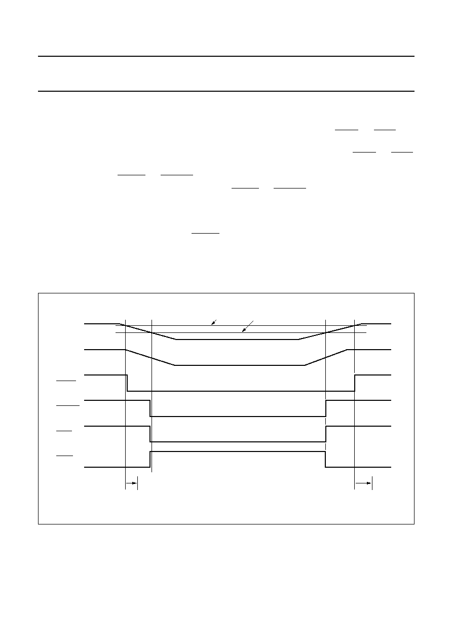
Fig.3 Example of external data read (standard firmware).
The timing is configurable under firmware control.
handbook, full pagewidth
MHB462
DMCS
RD
address bus
address/
data
ALE
internal
signals
XTAL1
address
external data
address

1999 Jun 04
14
Philips Semiconductors
Product specification
Global Positioning System (GPS)
baseband processor
SAA1575HL
Fig.4 Example of external data write (standard firmware).
The timing is configurable under firmware control.
handbook, full pagewidth
MHB463
DMCS
WRH/WRL
address bus
address/
data
ALE
internal
signals
XTAL1
address
external data
address
7.4.2
C
ODE MEMORY SPACE
The SAA1575HL has no internal code memory. The GPS
solution firmware resides in external memory. With the
standard Philips firmware, a ROM with a maximum access
time of 100 ns is required.
The classic operation of a multiplexed address/data bus
involves an address being set-up for every bus cycle.
The internal ALE signal is used to latch the address prior
to the cycle on which the data is set-up. An example of the
resulting timing is illustrated in Fig.5.
The SAA1575HL does not require an internal ALE cycle for
each code fetch. The lowest 3 address lines are not
multiplexed with the data lines and so these can be used
to incrementally read code locations.
The XA core can therefore issue up to 8 word reads
through sequential code memory for each ALE cycle. This
is termed a burst code read. An example of the resulting
timing is illustrated in Fig.6.
Any type of branch or jump in the program may require a
code fetch in a non-sequential manner and a new ALE
cycle will be needed. This may occur at any stage in a
code read. Thus the length of the read strobe in a burst
read is not necessarily an integer multiple of the individual
code read length.

1999 Jun 04
15
Philips Semiconductors
Product specification
Global Positioning System (GPS)
baseband processor
SAA1575HL
Fig.5 Example of code read with ALE (standard firmware).
The timing is configurable under firmware control.
handbook, full pagewidth
MHB464
DATA BUS
PMCS
address bus
address/
data
ALE
internal
signals
XTAL1
address
data input
address
Fig.6 Example of burst mode code read (standard firmware).
The timing is configurable under firmware control.
handbook, full pagewidth
MHB465
DATA BUS
PMCS
address
bus
address/
data
ALE
internal
signals
XTAL1
address 1
address 2
address 2
address 1
code word 2
code word 1

1999 Jun 04
16
Philips Semiconductors
Product specification
Global Positioning System (GPS)
baseband processor
SAA1575HL
7.5
CPU peripheral features
The SAA1575HL contains the hardware for 3 timers,
2 UARTs, a watchdog timer, a 3-bit RF IC programming
link and an 8-bit general purpose I/O port.
7.5.1
T
IMERS
/
COUNTERS
The SAA1575HL has 2 standard 16-bit timer/counters and
a third 16-bit up/down timer/counter. These timer/event
counters can perform the following functions:
·
Measure time intervals and pulse duration
·
Count external interrupts
·
Generate interrupt requests
·
Generate Pulse Width Modulation (PWM) or timed
output waveforms.
The timers are used by the standard Philips firmware to
generate the baud rates for the UART serial ports.
The additional features are not used in the standard
Philips firmware but are available for use in custom
firmware revisions.
All of the timers are configured in the 16-bit auto-reload
mode of operation. Timer 1 is used to generate the baud
rate for UART0 and Timer 2 is used to generate the baud
rate for UART1. In the standard Philips firmware, Timer 0
is not used.
7.5.2
W
ATCHDOG TIMER
The watchdog timer protects the system from incorrect
code execution by causing a processor reset if the
watchdog timer underflows as a result of a failure of the
firmware to feed the timer prior to it reaching its terminal
count.
In the standard Philips firmware, the watchdog is enabled
with a time-out period of 130 ms (at a clock frequency of
30 MHz).
7.5.3
UART
S
The SAA1575HL contains 2 UART ports, compatible with
the enhanced UART modes 1 to 3 on the 8xC51FB
(mode 0 operations not supported). With the exception of
the removal of the mode 0 operation, the UARTs in the
SAA1575HL are identical to those in the XA-G3 product.
Each UART rate is determined by either a fixed division of
the oscillator (in UART mode 2) or by one of the timer
overflow rates (in UART modes 1 and 3).
With the standard Philips firmware, both UARTs are
configured to be in Mode 1: variable rate 8-bit operation.
Ten bits are transmitted (via TXDn) or received
(via RXDn): a START bit, 8 data bits (LSB first), and a
STOP bit.
In general, the UART clocks (which are 16 times the baud
rate) are determined by the Timer 1 or Timer 2 overflow
rate. With the standard Philips firmware, Timer 1 is used to
generate the baud rate for UART0 and Timer 2 is used to
generate the baud rate for UART1. The baud rate is set to
be 4800 bits/s for both UARTs.
7.5.4
RF IC
PROGRAMMING PORT
The SAA1575HL is capable of programming the
UAA1570HL via a standard 3-wire serial link. This consists
of a clock line (SCLK), data line (D15 to D0) and a latch
enable (RFLE). Data is clocked into a holding register in
the UAA1570HL serially on each rising edge of the output
RFCLK. Once the complete serial packet has been
clocked into the RF IC, the latch enable output, RFLE, is
asserted which copies the new word from the holding
register in the RF IC into the control registers.
Proper timing of the clock, data and latch outputs is
ensured by firmware. An example sequence is illustrated
in Fig.7. The signals shown would result in the value 1001
being loaded into the last 4 bits of the RF IC serial register.
Each loading operation of the RF IC reloads the complete
RF control register.
With the standard Philips firmware, a 20-bit long word
0X5E320 is transmitted in this manner on start-up or
re-initialization. This gives full compatibility with the Philips
UAA1570HL front-end IC. See the
"UAA1570HL" for more
details about the configuration options of the front-end IC.

1999 Jun 04
17
Philips Semiconductors
Product specification
Global Positioning System (GPS)
baseband processor
SAA1575HL
7.5.5
G
ENERAL PURPOSE
I/O
The SAA1575HL possesses an 8-bit general purpose I/O register and 8 associated I/Os (see Fig.8). With the standard
Philips firmware, all 8 of these pins are configured as outputs.
With the standard Philips firmware, only pin GPIO0 is used. This is switched on at the end of the firmware initialization
sequence and remains on subsequently.
Fig.7 Example timing for UAA1570HL programming.
X = don't care.
handbook, full pagewidth
MHB466
RFCLK
RFDAT
control
holding
RFLE
1001
XXXX
XX10
1001
XXX1
X100
XXXX
Fig.8 GPIO pin drive circuits.
handbook, full pagewidth
MHB467
IOn
pull-up
FET
VCC(P)
GPIOn
pin
CLK
EN
D
DATA BUS
Q
WRITE ENABLE
READ ENABLE
CFGn
10
µ
A
1999 Jun 04
18
Philips Semiconductors
Product specification
Global Positioning System (GPS)
baseband processor
SAA1575HL
7.6
The real-time clock
The Real-Time Clock (RTC) is a functional unit used to
generate time information. Its purpose is to supply
approximate GPS time to the system firmware for the initial
acquisition of satellites (a warm start). The power supply
for the RTC is separate from the rest of the IC, allowing a
low capacity battery to be used to maintain the low power
RTC function.
The timebase for the RTC should be provided by a
dedicated 32.768 kHz crystal which can be omitted if the
RTC is not required. This is divided down by a fixed divider
to provide the 1 Hz timebase used for the rest of the RTC
block. A digital sampling circuit is also included to prevent
digital noise due to the on-chip processor causing
incorrect timekeeping.
The SAA1575HL uses a digital under-sampling system to
ensure that ground bounce does not cause RTC
timekeeping errors. This places a restriction on the ratio of
XTAL1 and XTAL3 frequencies for which the RTC will
operate correctly. This has been optimistic for the case
f
XTAL1
= 30 MHz, f
XTAL3
= 32 kHz and, assuming that the
RTC crystal frequency will always be 32 kHz, will operate
correctly for the entire specified range of system
frequencies.
Fig.9 Real-time clock circuit.
handbook, full pagewidth
MHB468
32 kHz
OSCILLATOR
XTAL4
XTAL3
XTAL
C
C
off-chip
(optional)
32 kHz
SAMPLER
system clock
1 Hz
PRE-SCALER
REAL-TIME
CLOCK COUNTERS

1999 Jun 04
19
Philips Semiconductors
Product specification
Global Positioning System (GPS)
baseband processor
SAA1575HL
7.7
The external bus
The off-chip memories and the on-chip registers are on the
same address and data bus. The routing of the data and
address signals between the on-chip registers and the
off-chip memories is controlled by a block known as the
external bus interface. In addition, certain chip enable
signals are decoded within the block to reduce the amount
of external glue logic required in the complete system.
The address latch, normally required on 80C51 systems,
is implemented within the SAA1575HL. Therefore, no ALE
signal is seen outside the IC and address and data lines
are brought out on separate pins.
However, since internally there is still the need to latch the
address from a common address/data bus, signals on the
data bus will be seen to change during the address set-up
cycles.
The lower 3 external address lines are driven directly by
the XA core and are not latched. This allows `burst' code
reads to be performed in which adjacent code locations
are accessed without the need for an address latch cycle.
Signals similar to those used by a standard 80C51 or XA
system are used to control the external bus activity.
Fig.10 SAA1575HL internal address and data routing.
handbook, full pagewidth
MHB469
ADDRESS
DECODER
LE
ALE
A4 to A19
D15 to D0
A3 to A1
ADDRESS
LATCH
XA
PMCS
WRH, WRL, RD
A3 to A1
D15 to D0
D15 to D0
to MMRS
ENABLE
A4 to A19
A1 to A8
PMCS
WRH, WRL, RD
DMCS
16
16
3
3
16
1999 Jun 04
20
Philips Semiconductors
Product specification
Global Positioning System (GPS)
baseband processor
SAA1575HL
7.7.1
P
ROGRAM MEMORY CHIP SELECT
This signal (PMCS) is an active LOW strobe used to
enable the output of the external code memory. It remains
HIGH when a read code is not in progress.
7.7.2
D
ATA MEMORY CHIP SELECT
This signal (DMCS) is an active LOW strobe used to
enable the external data memory. The SAA1575HL
hardware supports two distinct modes of operation of this
signal (selected in firmware) designed for optimum power
or optimum speed. The standard Philips firmware is
configured for optimum power.
DMCS is taken LOW during an external data read or write
operation to segments 0 to 14 of the memory map.
To prevent the corruption of external data memory, the
DMCS pin is driven on the backup supply voltage and will
be held HIGH once the PWRFAIL signal has been
asserted LOW.
With the standard Philips firmware, the DMCS signal is
gated by the external access read and write strobes. This
should significantly reduce the power consumption of the
external RAM but may require the use of a slightly faster
external memory (depending on clock speed and details of
the external memory used).
7.7.3
R
EAD STROBE
This signal (RD) is an active LOW strobe used to indicate
that the XA is expecting data from the external bus.
7.7.4
W
RITE
LOW
BYTE STROBE
This signal (WRL) is an active LOW strobe used to indicate
that the XA is performing an external write. This strobe
only applies to the lower data byte of the 16-bit data word,
allowing byte writes to be performed from the 16-bit data.
This strobe will also be taken LOW for word write
operations.
7.7.5
W
RITE
HIGH
BYTE STROBE
This signal (WRH) is an active LOW strobe used to
indicate that the XA is performing an external write. This
strobe only applies to the higher data byte of the 16-bit
data word, allowing byte writes to be performed from the
16-bit data. This strobe will also be taken LOW for word
write operations.
7.8
Backup supplies and reset
The SAA1575HL is designed to operate correctly in
situations when the main power supply fails. In addition to
the main core and peripheral power supplies, separate
pins are provided for backup core and peripheral supplies
which enable critical (and low-power) functions to be
maintained during the loss of main power. There is also an
on-chip reset timer which will aid the design of a full
power-down strategy.
7.8.1
S
UPPLY DOMAINS
To allow for the use of inexpensive 5 V external
components, the periphery of the SAA1575HL can be
powered with a higher voltage than the core. Therefore
there is a distinction between the core and peripheral
power supplies. In addition, there is the need to maintain
certain functionality on a low-power supply in the event of
main power failure. Therefore there are 2 additional
supplies required for so-called backup operation. Thus
there are four distinct power supply domains, two for the
core supplies and two for the peripheral supplies.
Table 1
Supply domains
In normal operation, the backup core and pad supplies
should be provided from the main power supply rather than
a low-capacity battery since the power drawn on the
backup supplies while the processor is operating may be
significant. Two output pins, PWRM and PWRB are
provided to control this switching.
SUPPLY
DESCRIPTION
PURPOSE
V
CC(core)
main core
supply (3 V)
provides power for all core
circuits, excluding those
mentioned below
V
CC(P)
main peripheral
supply
(3 to 5 V)
provides power for all pins,
excluding those mentioned
below
V
CC(R)
RTC core
supply
(2.4 to 3 V)
powers the real-time clock,
the 32 kHz oscillator and
the 32 kHz de-bounce
circuit; it also produces the
signals for DMCS, PWRM
and PWRB
V
CC(B)
backup
peripheral
supply
(2.4 to 5 V)
provides power for the
following pins: DMCS,
PWRM, PWRB and
PWRFAIL
1999 Jun 04
21
Philips Semiconductors
Product specification
Global Positioning System (GPS)
baseband processor
SAA1575HL
The power consumption of the SAA1575HL in the
power-down mode is minimal since no outputs are
changing. The only active circuit in power-down is the
real-time clock.
Isolation between the power domains is controlled by the
PWRFAIL input pin. This must be driven LOW in a
power-failure situation to ensure that the backup domains
are isolated from the main supply domains. If this is not
done, it is possible that the registers contained in the
backup supply domain will be corrupted as the main supply
is cycled. It is also possible that under these
circumstances a high backup supply current will be drawn
(depending on details of the external supply circuitry).
7.8.2
P
OWER
-
DOWN DESIGN STRATEGY
In power-down operation the main supplies are assumed
to have failed. The backup core and pad supplies should
be switched to backup power. The detection of the power
failure and the power supply switching is the responsibility
of the user. However, the SAA1575HL does provide
several functions to aid this task.
The power-down and power-fail operations of the
SAA1575HL are controlled by two inputs, PWRDN and
PWRFAIL, which are assumed to be connected to external
voltage comparators. The use of external comparators
allows the voltage thresholds to be set by the system
designer. It also allows a certain amount of flexibility as to
which supplies are monitored for power failure.
7.8.2.1
Power-down control signals
The power-down control signal pins (see Table 2) are
either inputs or outputs associated with the SAA1575HL
power control. The descriptions are for the intended use of
the control signals in a normal application.
For a correct reset to occur, it is important that PWRFAIL
should be held LOW as long as minimum voltages have
been established on all four of the power supply domains.
If this is not done various serious consequences may
occur, including main oscillator failure, a high supply
current state, a processor crash or RTC register
corruption.
Table 2
Power-down control signals
SIGNAL
FUNCTION
PWRDN
Power-down indicator: this should be driven LOW by an external comparator to indicate impending
power failure. Internally it sends an interrupt to the processor used to initiate a power-fail routine. At the
end of this routine the standard firmware forces the processor into reset. This also inhibits the external
RAM chip select. Reset is only de-asserted a set time after both PWRDN and PWRFAIL go HIGH,
controlled by the RSTIME input.
PWRFAIL
Power fail indicator: this should be driven LOW by an external comparator to indicate immediate power
failure. Internally it forces immediate reset of the processor, isolation of the RTC and inhibition of the
external RAM chip select. It also controls the power switch outputs PWRB and PWRM. Reset is only
de-asserted a set time after both go HIGH, controlled by the RSTIME input.
RSTIME
Reset timer control: this sets the time delay between de-assertion of both PWRDN and PWRFAIL and
the de-assertion of the processor reset. If HIGH, the delay is approximately 10 ms. If LOW the delay is
approximately 10
µ
s.
DMCS
External RAM chip select: this is driven via the backup supplied core and pads. In power-down this is
isolated from the rest of the IC and the output held HIGH to prevent corruption of the external RAM.
PWRM
Main power supply control: in normal operation this is held LOW. This can be used to switch the main
supplies to all of the supply input pins. In normal operation the backup pad supply pin should be driven
by the main supply and the backup core supply pins should be driven by the main core supply. When the
IC goes into power-down mode this output goes HIGH. In power-down the backup supply pins should be
driven by their appropriate supplies.
PWRB
Backup power supply control: this is the inverse of PWRM
1999 Jun 04
22
Philips Semiconductors
Product specification
Global Positioning System (GPS)
baseband processor
SAA1575HL
7.8.2.2
Example of strategy for slow supplies
The ultimate use of the power control signals is up to the
user. However, two possibilities are presented as design
examples. The first example will operate correctly in
circuits where the rise times of the power supplies is slow
compared to any delay between the supplies to the
peripheral and core power domains.
In this example, both the PWRDN and PWRFAIL logic
inputs to the SAA1575HL are derived by comparing the
V
CC(P)
supply voltage against known references.
In general, since it is a lower voltage, the V
CC(core)
supply
may hold and reach it's nominal voltage quicker than the
V
CC(P)
supply.
As V
CC(P)
falls, the first threshold is reached and PWRDN
is taken LOW. This triggers an interrupt in the firmware
which is used to perform any required housekeeping. It is
assumed that there is time for this to be completed before
complete supply failure.
At the end of the interrupt routine, the firmware places the
SAA1575HL into reset. As V
CC(P)
continues to fall, the
second threshold is reached and is taken LOW. This
toggles the power controls, both PWRM and PWRB, and
will force a reset if it has not already occurred.
On power-up, the power controls both PWRM and PWRB
will be switched once the second threshold voltage is
reached. As the supply voltage rises further, the first
voltage threshold will be reached at which time both
PWRDN and PWRFAIL will be HIGH. This starts the reset
counter and the SAA1575HL will remain in reset until a set
time after this, depending on the state of the input pin
RSTIME.
Fig.11 Example of power-down strategy with slow supplies.
handbook, full pagewidth
MHB470
PWRB
delay while XA in
interrupt routine
reset timer delay
set by RSTIME
Vt1
VCC(P)
VCC(core)
Vt2
PWRFAIL
PWRDN
PWRM

1999 Jun 04
23
Philips Semiconductors
Product specification
Global Positioning System (GPS)
baseband processor
SAA1575HL
7.8.2.3
Example of strategy for fast supplies
The second example will operate correctly in circuits
where the delay between the supplies to the peripheral
and core power domains is significant compared to the rise
times of the power supplies. This may occur in cases
where the core supply is a regulated (delayed) version of
the peripheral supply. If the previous strategy were used in
this situation, it would be possible for the SAA1575HL to
miss the PWRFAIL LOW state at power-up, resulting in the
IC not being given a correct reset.
In this example, the PWRDN logic input is derived as
before by comparing the V
CC(P)
supply voltage against a
known reference voltage. But in this instance the
PWRFAIL logic input is derived by comparing the V
CC(core)
core supply against a threshold voltage.
As V
CC(P)
falls, the first threshold level is reached and
PWRDN is taken LOW. This triggers an interrupt in the
firmware which is used to perform any required
housekeeping. At the end of the interrupt routine, the
firmware places the SAA1575HL into reset.
However, if the fall times on the supplies is fast, it is likely
that the PWRFAIL input will go LOW before the interrupt
routine has been completed. This would force the
SAA1575HL into immediate reset. At this time both PWRM
and PWRB toggle to switch backup supply sources.
On power-up, the V
CC(P)
supply rises quickly. However,
since this only controls an interrupt flag and the
SAA1575HL is still held in reset by PWRFAIL, this has no
effect. Only once the V
CC(core)
supply rises will PWRFAIL
be de-asserted. This can only occur once the V
CC(core)
voltage has reached the set threshold, and so there is no
risk of the IC `missing' the reset pulse. The SAA1575HL
will come out of reset a set time after this, depending on
the state of the input pin RSTIME.
Fig.12 Example of power-down strategy with fast supplies.
handbook, full pagewidth
MHB471
PWRB
delay while XA in
interrupt routine
reset timer delay
set by RSTIME
Vt1
Vt3
VCC(P)
VCC(core)
PWRFAIL
PWRDN
PWRM

1999 Jun 04
24
Philips Semiconductors
Product specification
Global Positioning System (GPS)
baseband processor
SAA1575HL
7.8.3
S
YSTEM RESET CONTROL
The SAA1575HL contains an internal timer and control
logic to perform various system reset tasks. Control of this
logic is by three external pins, PWRDN, PWRFAIL, and
RSTIME. This allows the system designer to set the
voltage thresholds at which the system goes into and
comes out of reset.
7.8.3.1
The reset timer
The heart of the reset system is a 20-bit counter with
asynchronous reset, clocked from the XTAL1 system
clock. The reset counter is asynchronously reset if the
PWRFAIL pin is LOW. Once reset, the counter will only be
enabled once both PWRFAIL and PWRDN go HIGH. This
prevents the SAA1575HL from leaving the reset state until
both power detect inputs have flagged the power system
as healthy.
The internal reset signal is generated by decoding the
reset counter. The decode value, and hence the time
delay, is controlled by the reset time control pin, RSTIME.
Table 3
Reset time control
The internal reset is de-asserted a given number of XTAL1
clock cycles after PWRFAIL and PWRDOWN go HIGH.
It is suggested that for most applications RSTIME should
be held HIGH, giving a reset time of approximately 10 ms.
This would be needed to allow the on-chip oscillator to
stabilize after power-up. The shorter reset time can be
used for applications using an external XTAL1 clock signal
which does not need a long stabilization period.
It is important that PWRFAIL should be LOW during
power-up of the IC to give the correct reset.
RSTIME
INPUT
NUMBER OF
CYCLES BEFORE
RESET
DE-ASSERTED
TIME DELAY
(f
XTAL1
= 30 MHz)
1
294 912
9.8 ms
0
288
9.6
µ
s
7.8.3.2
Overall reset operation
The assertion of the reset signal (by means already
described) will cause the following to occur:
·
Internal XA processor reset
·
Internal registers reset
·
Data bus pins set to be inputs
·
Read and write strobes de-asserted
·
GPIO pins set to be inputs
·
On-chip XTAL1 oscillator enabled.
7.8.3.3
CPU reset operation
Assuming that the correct external PWRFAIL sequence is
generated on power-up, the internal XA will receive the
correct reset signal from the on-chip reset block. If the
proper PWRFAIL is not performed, the operation of the
on-chip reset block cannot be guaranteed and the XA may
fail wholly or in part.
The embedded XA requires a minimum length of reset to
complete the various tasks. This minimum length is
guaranteed by the on-chip reset block. The only restriction
on the length of the pulse is that is should be long enough
to be asynchronously detected by the SAA1575HL
(typically 10 ns).
The embedded CPU can also be reset by the watchdog
timer (this may be disabled on some custom firmware
revisions).
7.8.4
P
OWER SAVING MODES
The SAA1575HL supports two power saving modes; Idle
mode and sleep mode. Both modes are selected by
firmware (or message over the serial link if included in the
firmware). In addition, the input to any of the correlators
can be inhibited individually (by firmware) which will
reduce the power consumed by the block to only the clock
tree dissipation.

1999 Jun 04
25
Philips Semiconductors
Product specification
Global Positioning System (GPS)
baseband processor
SAA1575HL
7.8.4.1
Sleep mode
The sleep mode is intended to overlay the function of the
standard 80C51XA Idle mode. Sleep is initiated by a
firmware or external serial link command. This initiates a
firmware routine which performs the following:
1. Send serial command to power-down RF IC
(UAA1570HL)
2. Inhibit RCLK, IF2 and IF1 inputs to SAA1575HL
3. Enter standard 80C51XA Idle state.
In sleep mode the RCLK and IF inputs are prevented from
entering the IC. This capability is included to cover the
situation in which the SAA1575HL is used with a front-end
which does not respond to the power-down command in a
similar way to the UAA1570HL. Sleep mode can be exited
by any active hardware interrupt, for example a UART
interrupt. The sleep mode has no effect on the operation of
the RTC.
7.8.4.2
Idle mode
The Idle mode is initiated by a firmware or external serial
link command. This is a direct use of the standard
80C51XA Idle mode. The interrupt signals from the active
peripherals such as UARTs, timers, host interface and
external interrupts will cause the CPU to resume execution
from the point at which it was halted. In the Idle mode, all
of the output pins retain their logic states from their
`pre-idle' position. No other action is taken on entering Idle
mode. In particular, the correlators will remain active since
RCLK, IF1 and IF2 will not be prevented from entering the
IC.
7.9
Clock signals and oscillators
The SAA1575HL requires 3 clock signals for full operation:
·
XTAL1: Processor (system) clock
·
XTAL3: Real-time clock crystal frequency (optional)
·
RCLK: GPS reference clock.
Two of these clocks, XTAL1 and XTAL3, can be generated
by on-chip oscillator circuits. The third, RCLK, must be
supplied from an external source; in most applications a
temperature compensated oscillator module.
7.9.1
S
YSTEM CLOCK
(XTAL1)
The SAA1575HL requires a system clock for the on-chip
processor and related peripheral blocks. This can be
provided from an external clock source via the XTAL1
input pin or by using the on-chip oscillator circuit with an
external resonating element connected between the
XTAL1 and XTAL2 pins. In most circumstances this would
be an external crystal accompanied by two capacitors
connected to ground, a series resistor (to optimize power
consumption) and a shunt resistor to ensure start-up under
all conditions.
Optimum values of C, R
P
and R
S
will depend on the crystal
used. However, typical values would be C = 20 pF,
R
P
= 1 M
and R
S
= 200
. The hardware places a
restriction on the range of frequencies for which correct
operation will occur; 26 MHz < f
XTAL1
< 32 MHz.
However, the restriction on operating frequency imposed
by the firmware is tighter than this. The standard Philips
firmware has been written on the assumption of a 30 MHz
system clock frequency.
Fig.13 System clock oscillator circuit.
handbook, halfpage
MHB472
OSCILLATOR
XTAL2
XTAL1
XTAL
C
C
off-chip
on-chip
RP
(optional)
RS
(optional)
system
clock

1999 Jun 04
26
Philips Semiconductors
Product specification
Global Positioning System (GPS)
baseband processor
SAA1575HL
7.9.2
RTC
CLOCK
(XTAL3)
If the on-chip real-time clock is required (as with the
standard Philips firmware), a low frequency clock signal is
required to run the clock. The SAA1575HL is designed so
that a standard 32.768 kHz watch crystal can be used for
this purpose. Since this is much slower than the system
clock, a much lower power is required to run just the
real-time clock, allowing it to be powered from a
low-capacity battery when the main power supply fails.
As with the system clock, there is an on-chip oscillator so
that only a few passive external components are required.
These would be an external crystal accompanied by two
capacitors connected to ground, a series resistor
(optional) and a shunt resistor to ensure start-up under all
conditions.
Optimum values of C and R
P
will depend on the crystal
used. However, typical values would be C = 22 pF and
R
P
= 1 M
.
7.9.3
R
EFERENCE CLOCK
(RCLK)
The reference clock input, RCLK, is used as the source for
the sampling of the IF input signal. A divided-down version
of RCLK is output on the sample clock pin, SCLK, for use
by the front-end IC.
The division ratio of RCLK/SCLK is programmable in
firmware. In the standard Philips firmware this ratio is set
to 3.
Fig.14 RTC clock oscillator circuit.
handbook, halfpage
MHB473
OSCILLATOR
XTAL4
XTAL3
XTAL
C
C
RP
(optional)
RTC clock
off-chip
on-chip
1999 Jun 04
27
Philips Semiconductors
Product specification
Global Positioning System (GPS)
baseband processor
SAA1575HL
8
LIMITING VALUES
In accordance with the Absolute Maximum Rating System (IEC 134).
Notes
1. Human body model: C = 100 pF; R = 1.5 k
.
2. Machine model: C = 200 pF; L = 0.75
µ
H; R = 0
.
9
THERMAL CHARACTERISTICS
SYMBOL
PARAMETER
CONDITIONS
MIN.
MAX.
UNIT
V
CC(core)
core supply voltage
-
0.5
+3.6
V
V
CC(R)
RTC core supply voltage
-
0.5
+3.6
V
V
CC(P)
peripheral DC supply voltage
-
0.5
+5.5
V
V
CC(B)
backup peripheral DC supply voltage
-
0.5
+5.5
V
V
CC
absolute voltage differences between two V
CC
pins
-
550
mV
P
tot
total power dissipation
-
500
mW
T
stg
storage temperature
-
65
+150
°
C
T
j
junction temperature
-
150
°
C
T
amb
ambient temperature
V
CC(core)
= V
CC(R)
= 3.3 V;
V
CC(P)
= V
CC(B)
= 5.0 V
-
40
+85
°
C
V
es
electrostatic handling
note 1
2000
-
V
note 2
200
-
V
SYMBOL
PARAMETER
CONDITIONS
VALUE
UNIT
R
th(j-a)
thermal resistance from junction to ambient
in free air
45
K/W
1999 Jun 04
28
Philips Semiconductors
Product specification
Global Positioning System (GPS)
baseband processor
SAA1575HL
10 DC CHARACTERISTICS
V
CC(P)
= V
CC(B)
= 5 V; V
CC(core)
= V
CC(R)
= 3 V; T
amb
= 20
°
C; f
osc
= 30 MHz; standard Philips firmware (release HD00);
note 1; unless otherwise specified.
SYMBOL
PARAMETER
CONDITIONS
MIN.
TYP.
MAX.
UNIT
Supplies
V
CC(core)
core supply voltage
2.7
3.3
3.6
V
V
CC(P)
peripheral supply voltage
2.7
5.0
5.5
V
V
CC(R)
RTC core supply voltage
2.4
3.3
3.6
V
V
CC(B)
backup peripheral supply voltage
2.7
5.0
5.5
V
I
CC(core)
core supply current
normal mode
-
35
-
mA
idle mode
-
15
-
mA
sleep mode
-
-
10
µ
A
I
CC(P)
peripheral supply current
normal mode; note 2
-
20
-
mA
idle mode
-
-
1
mA
sleep mode
-
-
1
mA
I
CC(R)
RTC core supply current
normal mode; note 3
-
10
30
µ
A
idle mode; note 3
-
10
30
µ
A
sleep mode; note 3
-
10
30
µ
A
I
CC(B)
backup peripheral supply current
normal mode; note 2
-
5
-
mA
idle mode
-
1
-
µ
A
sleep mode
-
1
-
µ
A
Inputs: pins PWRFAIL, PWRDN, RSTIME, RXD1, RXD0, IF2, IF1, RCLK, TEST1, TP1, TP2, TP3 and TP4
V
IL
LOW-level input voltage
-
-
1.5
V
V
IH
HIGH-level input voltage
3.5
-
-
V
Outputs (LOW drive current): pins PWRB, PWRM, T1S, RFCLK, RFDAT, RFLE and TEST2
V
OL
LOW-level output voltage
I
OL
= 2.0 mA
-
-
0.4
V
V
OH
HIGH-level output voltage
I
OH
= 0.5 mA
2.4
-
-
V
I
drive(max)
maximum drive current
-
-
2
mA
C
L(max)
maximum load capacitance
-
-
50
pF
t
d(t)
transition delay
C
L
= 5 pF
-
7.4
-
ns
C
L
= 25 pF
-
8.8
-
ns
Outputs (HIGH drive current): pins A19 to A1, DMCS, PMCS, TXD0, TXD1 and SCLK
V
OL
LOW-level output voltage
I
OL
= 4.0 mA
-
-
0.4
V
V
OH
HIGH-level output voltage
I
OH
= 1.0 mA
2.4
-
-
V
I
drive(max)
maximum drive current
-
-
4
mA
C
L(max)
maximum load capacitance
-
-
100
pF
t
d(t)
transition delay
C
L
= 10 pF
-
6.8
-
ns
C
L
= 50 pF
-
8.1
-
ns

1999 Jun 04
29
Philips Semiconductors
Product specification
Global Positioning System (GPS)
baseband processor
SAA1575HL
Notes
1. XTAL1, XTAL2, XTAL3 and XTAL4 are not specified with respect to levels.
2. Depends on all the external circuit driven by outputs.
3. Specified at RTC clock frequency of 32.768 kHz.
I/O: pins WRL, WRH and RD
V
IL
LOW-level input voltage
-
-
1.5
V
V
IH
HIGH-level input voltage
3.5
-
-
V
V
OL
LOW-level output voltage
I
OL
= 4.0 mA
-
-
0.4
V
V
OH
HIGH-level output voltage
I
OH
= 1.0 mA
2.4
-
-
V
I
drive(max)
maximum drive current
-
-
4
mA
C
L(max)
maximum load capacitance
-
-
100
pF
t
d(t)
transition delay
C
L
= 10 pF
-
7.0
-
ns
C
L
= 50 pF
-
8.7
-
ns
I/O (pull-up): pins D15 to D0 and GPIO7 to GPIO0
V
IL
LOW-level input voltage
-
-
1.5
V
V
IH
HIGH-level input voltage
3.5
-
-
V
V
OL
LOW-level output voltage
I
OL
= 4.0 mA
-
-
0.4
V
V
OH
HIGH-level output voltage
I
OH
= 1.0 mA
2.4
-
-
V
I
drive(max)
maximum drive current
-
-
4
mA
C
L(max)
maximum load capacitance
-
-
100
pF
t
d(t)
transition delay
C
L
= 10 pF
-
8.9
-
ns
C
L
= 50 pF
-
11.0
-
ns
I
pu
pull-up current
-
10
-
µ
A
SYMBOL
PARAMETER
CONDITIONS
MIN.
TYP.
MAX.
UNIT
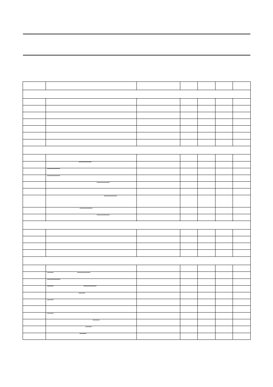
1999 Jun 04
30
Philips Semiconductors
Product specification
Global Positioning System (GPS)
baseband processor
SAA1575HL
11 AC CHARACTERISTICS
V
CC(P)
= V
CC(B)
= 5 V; V
CC(core)
= V
CC(R)
= 3 V; T
amb
= 20
°
C; f
osc
= 30 MHz; standard Philips firmware (release HD00);
unless otherwise specified.
SYMBOL
PARAMETER
CONDITIONS
MIN.
TYP.
MAX.
UNIT
External clock
f
osc
oscillator frequency
26
30
32
MHz
T
clk
clock period and CPU timing cycle
-
33.3
-
ns
t
CLKH
clock HIGH time
40 to 60% duty cycle
-
6.7
-
ns
t
CLKL
clock LOW time
40 to 60% duty cycle
-
6.7
-
ns
t
r(clk)
clock rise time
-
5
-
ns
t
f(clk)
clock fall time
-
5
-
ns
f
clk(ref)
reference clock frequency
-
14.4
35
MHz
External program memory read (non-burst code read); see Fig.16
t
AVAU
address valid time period
163.7
165.7
-
ns
t
AVPL
address valid to PMCS asserted
62.7
65.7
-
ns
t
W(PMCS)
PMCS pulse width
97.0
98.0
-
ns
t
PLIV
PMCS LOW to instruction valid
-
82.0
85.0
ns
t
h(I)
instruction hold time after PMCS de-asserted
0.0
-
-
ns
t
AVIV
address valid to instruction valid (access time)
-
148.7
151.7
ns
t
su(I)
instruction set-up time before PMCS
de-asserted
14.0
16.0
-
ns
t
PXIZ
bus 3-state after PMCS de-asserted
-
30.0
36.0
ns
t
h
hold time of a (3 : 1) after PMCS de-asserted
0.0
1.0
-
ns
External program memory read (burst code read); see Figs 16 and 17
t
AVAU
address valid time period
131.3
132.3
-
ns
t
AVIV
address valid to instruction valid (access time)
-
115.3
118.3
ns
t
IVAU
instruction valid to address undefined
15.0
17.0
-
ns
t
AUIU
address valid to instruction undefined
0.0
-
-
ns
External data memory read; see Fig.18
t
AVAU
address valid time period
163.7
164.7
-
ns
t
RLEL
RD asserted to DMCS asserted
note 1
-
2.0
4.0
ns
t
W(DMCS)
DMCS pulse width
97.0
98.0
-
ns
t
RHEH
RD de-asserted to DMCS de-asserted
-
2.0
6.0
ns
t
AVRL
address valid to RD asserted
64.7
65.7
-
ns
t
W(RD)
RD pulse width
98.0
-
-
ns
t
AVDV
address valid to data valid (access time)
-
148.7
151.7
ns
t
RLDV
RD asserted to data valid
-
82.0
85.0
ns
t
su(D)
data set-up time before RD de-asserted
15.0
16.0
-
ns
t
h(D)
data hold time after RD de-asserted
0.0
-
-
ns
t
RHDZ
bus 3-state after RD de-asserted
-
30.0
36.0
ns
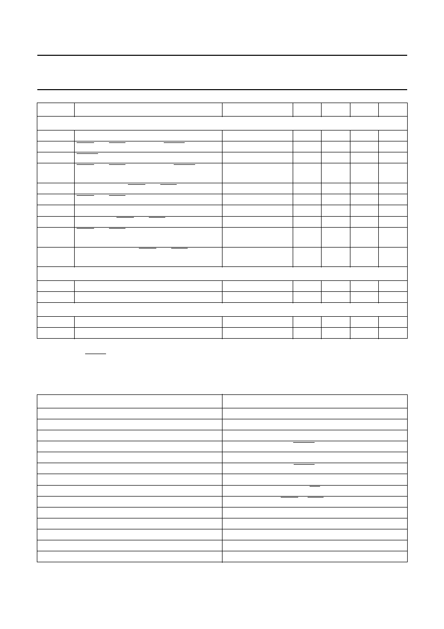
1999 Jun 04
31
Philips Semiconductors
Product specification
Global Positioning System (GPS)
baseband processor
SAA1575HL
Notes
1. For default DCMS operation.
2. The 1 s pulse output is only valid when at least one channel is locked.
Table 4
Explanation of symbol characters in Chapter "AC characteristics"
External data memory write; see Fig.19
t
AVAU
address valid time
164.7
-
-
ns
t
WLDL
WRH and WRL asserted to DMCS asserted
note 1
-
2.0
4.0
ns
t
W(DMCS)
DMCS pulse width
65.7
-
-
ns
t
WHDH
WRH and WRL de-asserted to DMCS
de-asserted
-
2.0
4.0
ns
t
AVWL
address valid to WRH and WRL asserted
63.7
-
-
ns
t
WLWH
WRH and WRL pulse width
64.7
65.7
-
ns
t
AVQV
address valid to data valid
67.7
-
-
ns
t
QVWL
data valid to WRH and WRL de-asserted
-
9.0
-
4.0
-
ns
t
WHAU
WRH and WRL de-asserted to address
undefined
2.0
-
-
ns
t
h(D)
data hold time after WRH and WRL
de-asserted
0
1.0
-
ns
GPS IF input timing; see Fig.20
t
FVSH
IF set-up time before rising edge of SCLK
-
10
-
ns
t
SHFV
IF hold time after rising edge of SCLK
0
-
-
ns
1 second pulse output; see Fig.21
t
W(T1S)
T1S pulse width
-
1.0
-
µ
s
T
T1S
T1S pulse period
note 2
-
1.0
-
s
SYMBOL CHARACTER
DESCRIPTION
A
address
C
clock
D
input data
E
DMCS strobe
I
instruction (program memory)
P
PCMS strobe
Q
output data
R
RD
W
WRH or WRL strobes
H
logic high
L
logic low
U
undefined
V
valid
Z
high impedance or pull-up
SYMBOL
PARAMETER
CONDITIONS
MIN.
TYP.
MAX.
UNIT
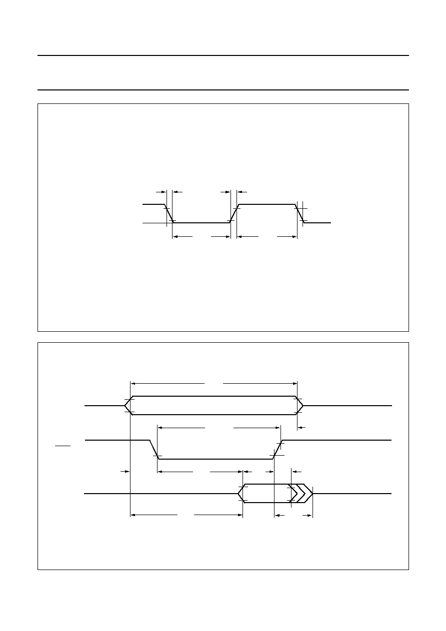
1999 Jun 04
32
Philips Semiconductors
Product specification
Global Positioning System (GPS)
baseband processor
SAA1575HL
Fig.15 External XTAL1 clock drive.
handbook, full pagewidth
MHB474
XTAL1
tCHCL
tCLCH
4.5 V
0.45 V
3.5 V
0.9 V
tCLKL
tCLKH
Fig.16 External program memory read cycle (non-burst).
handbook, full pagewidth
MHB475
D15 to D0
PMCS
A19 to A1
2.4 V
0.4 V
tAVIV
tAVAU
2.4 V
0.4 V
2.4 V
0.4 V
0.4 V
tAVPL
tW(PMCS)
tsu(l)
th(l)
tPLIV
tPXIZ
th
2.4 V
0.4 V

1999 Jun 04
33
Philips Semiconductors
Product specification
Global Positioning System (GPS)
baseband processor
SAA1575HL
Fig.17 External program memory read cycle (burst).
handbook, full pagewidth
MHB476
tIVAU
tAUIU
2.4 V
0.4 V
tAVAU
tAVIV
2.4 V
0.4 V
D15 to D0
PMCS
A19 to A1
Fig.18 External data memory read cycle.
Default DMCS operation.
handbook, full pagewidth
MHB477
RD
D15 to D0
DMCS
A19 to A1
2.4 V
0.4 V
tAVDV
tW(DMCS)
tRLEL
2.4 V
tAVAU
0.4 V
2.4 V
2.4 V
0.4 V
0.4 V
tAVRL
tW(RD)
tsu(D)
tRLDV
tRHDZ
tRHEH
2.4 V
0.4 V
DATA IN
th(D)
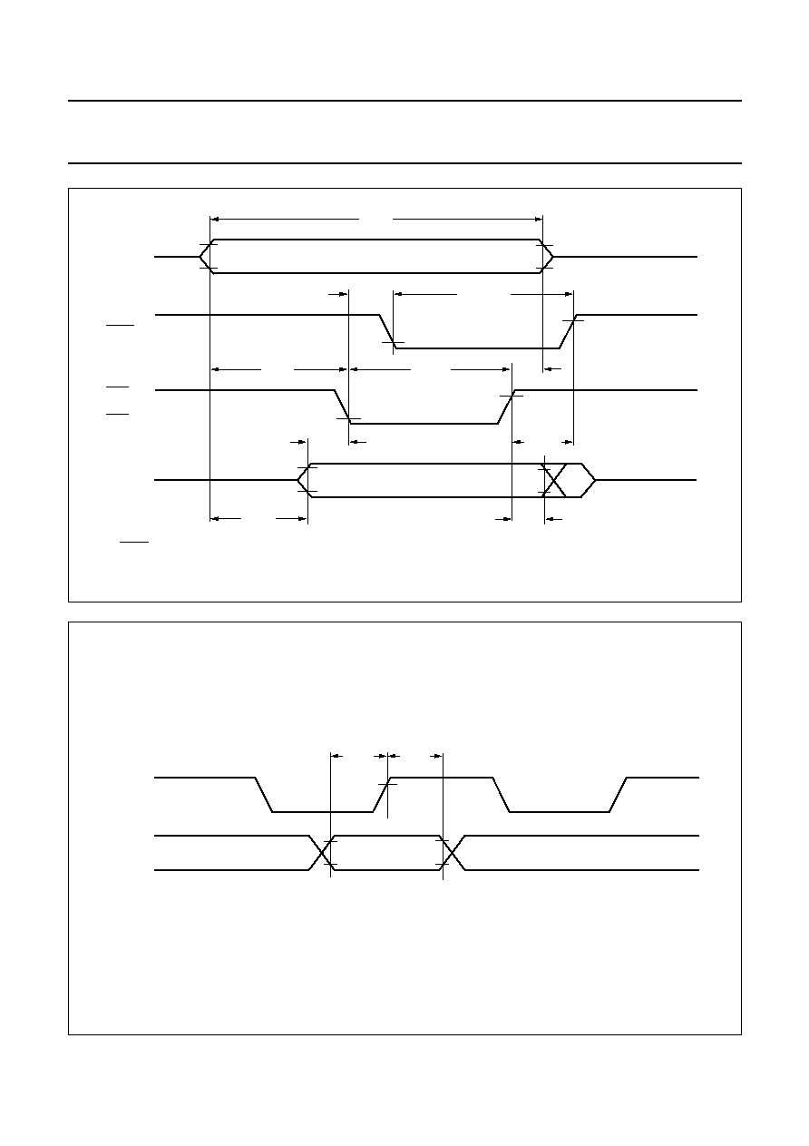
1999 Jun 04
34
Philips Semiconductors
Product specification
Global Positioning System (GPS)
baseband processor
SAA1575HL
Fig.19 External data memory write cycle.
Default DMCS operation.
handbook, full pagewidth
MHB478
WRH
or
WRL
D15 to D0
DMCS
A19 to A1
2.4 V
0.4 V
tAVQV
tW(DMCS)
tWLDL
2.4 V
tAVAU
0.4 V
2.4 V
2.4 V
0.4 V
0.4 V
tAVWL
tWLWH
tQVWL
tWHDH
th(D)
tWHAU
2.4 V
0.4 V
DATA OUT
Fig.20 IF input timing.
handbook, full pagewidth
MHB479
IF1, IF2
SCLK
tFVSH
tSHFV
2.4 V
0.4 V
2.4 V
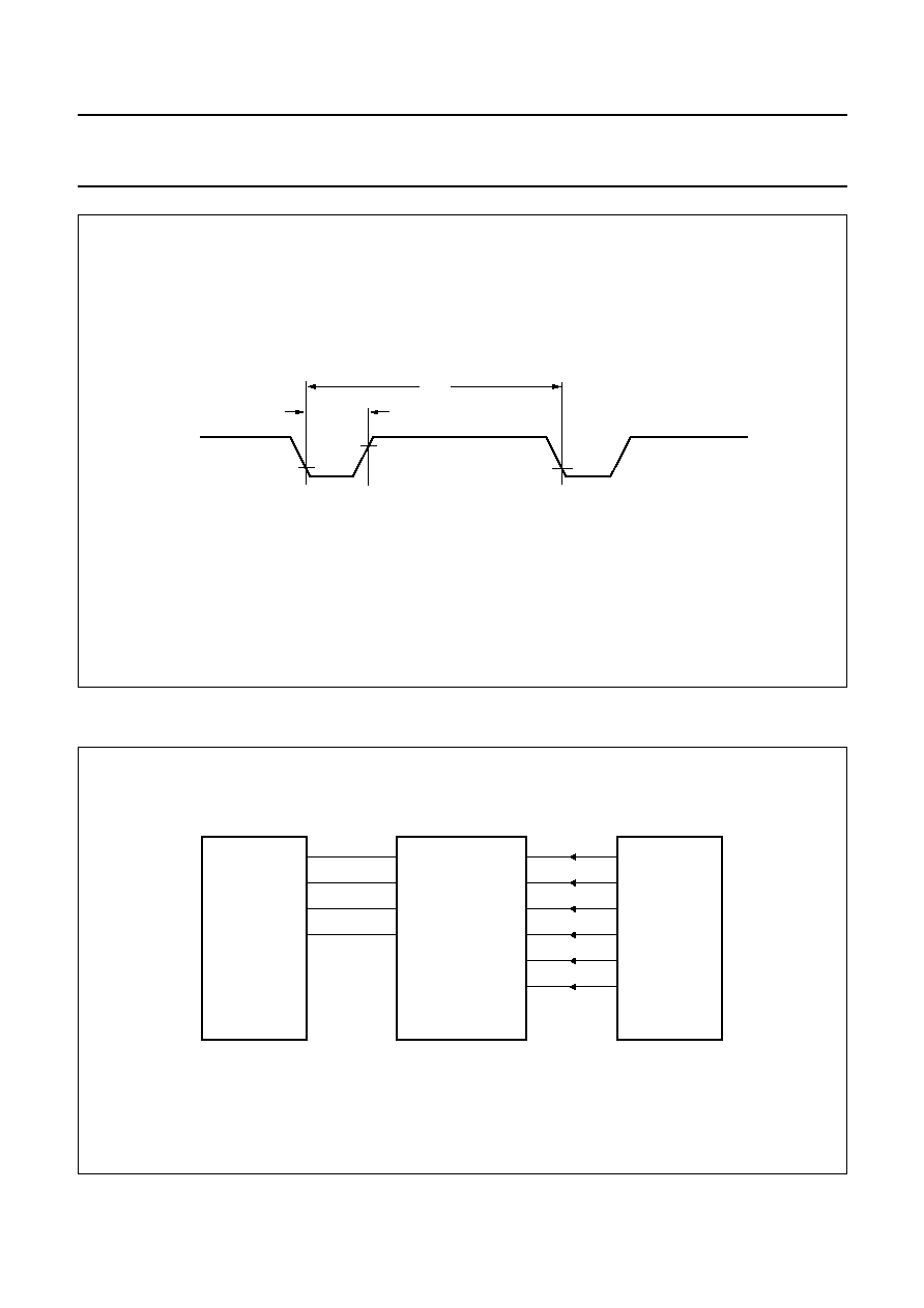
1999 Jun 04
35
Philips Semiconductors
Product specification
Global Positioning System (GPS)
baseband processor
SAA1575HL
12 DEFAULT APPLICATION AND DEMONSTRATION BOARD
Fig.21 T1S output pulse timing.
Signal may be inverted under firmware control.
handbook, full pagewidth
MHB480
T1S
tW(T1S)
2.4 V
0.4 V
0.4 V
TT1S
Fig.22 Overall schematic.
handbook, full pagewidth
MHB289
DIGITAL
PROCESSOR
RCLK
SCLK
SIGN
RFDATA
RFCLK
RFLE
RF
FRONT-END
RCLK
SCLK
SIGN
RFDATA
POWER
SUPPLY
VRTC
VBB
BATT_ON
BATT_OFF
VRTC
VBB
BATT_ON
BATT_OFF
RFCLK
RFLE
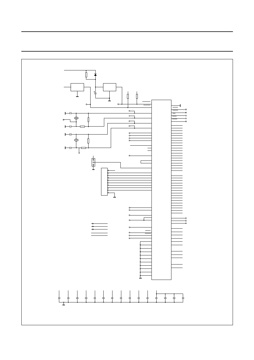
1999 Jun 04
36
Philips Semiconductors
Product specification
Global Positioning System (GPS)
baseband processor
SAA1575HL
Fig.23 Baseband circuitry (continued in Fig.24).
MHB290
handbook, full pagewidth
44
73
47
46
45
41
40
74
14
15
52
76
WRL
WRH
A1
TP1
PMCS
DMCS
RD
39
35
34
33
32
36
29
28
A6
A7
A8
A9
A2
A3
A4
A5
27
A10
24
22
21
20
19
23
18
11
A15
A16
A17
A18
A11
A12
A13
A14
10
A19
70
68
67
64
63
69
62
59
D4
D5
D6
D7
D0
D1
D2
D3
58
D8
57
55
54
53
56
D13
D9
D10
D11
D12
49
48
D14
D15
89
RFDAT
90
91
RFCLK
RFLE
16
25
37
51
61
86
VCC(P)
VCC(P)
VCC(P)
VCC(P)
VCC(P)
VCC(P)
VCC1
VCC2
VCC3
VCC4
VCC5
VCC6
12
30
66
VCC(core)
VCC(core)
VCC(core)
VDD1
VDD2
VDD3
72
80
VCC(B)
VCC(R)
VRTC1
VBB1
XTAL2
XTAL3
PWRFAIL
PWRDN
XTAL1
75
83
84
81
82
4
TxD1
RxD1
TP4
XTAL4
TxD0
RxD0
42
96
95
94
GPIO1
GPIO2
TP2
GPIO0
88
87
5
6
GPIO7
GPIO6
GPIO3
GPIO4
7
GPIO5
8
9
n.c.
n.c.
U204
SAA1575HL
R207
470
R206
10 k
D201
BAS16
RCLK
SCLK
SIGN
BATT_ON
BATT_OFF
RCLK
SCLK
SIGN
BATT_ON
BATT_OFF
VCC
VCC
VCC
VCC
R205
10 k
R204
1 M
VCC
10 pF
C207
C208
180
R203
VCC
VCC
1
JP202
HEADER 10
2
3
4
5
6
7
9
8
10
10 pF
JP201
JMP3
TP218
TP216
TP225
TP219
TP220
TP221
TP211
TP210
TP209
TP208
98
1
RCLK
SCLK
TP201
TP202
93
92
3
IF1
IF2
TP3
TP203
2
T1S
TP204
VCC
VCC
77
78
43
RSTIME
PWRB
PWRM
SIGN
T1S_OUT
BATT_ON
BATT_OFF
13
VSS
17
VSS
26
VSS
31
VSS
38
VSS
50
VSS
60
VSS
65
VSS
71
VSS
79
VSS
85
VSS
TP205
TP206
97
99
100
TEST1
TEST2
n.c.
TP207
TP222
TP223
TP224
1
2
3
VCC
OUT
GND
U207
ZM33164
TP217
TP229
1
2
3
VCC
OUT
GND
U206
ZM33064
C209
10
µ
F
(6.3 V)
Y201
30 MHz
R202
10 M
27 pF
C205
C206
0
R201
27 pF
TP212
TP213
TP214
TP215
TP230
Y202
32.678
kHz
GND
GND
GND
GND
GND
GND
GND
GND
GND
GND
VCC
C224
33 nF
C223
33 nF
C222
33 nF
C221
33 nF
VCC6
C220
33 nF
VCC5
C219
33 nF
VCC4
C218
33 nF
VCC3
C217
33 nF
VCC2
C216
33 nF
VCC1
C215
33 nF
VRTC1
C214
33 nF
VBB1
C213
33 nF
VDD3
C212
33 nF
VDD2
C211
33 nF
VDD1
C210
33 nF
GND
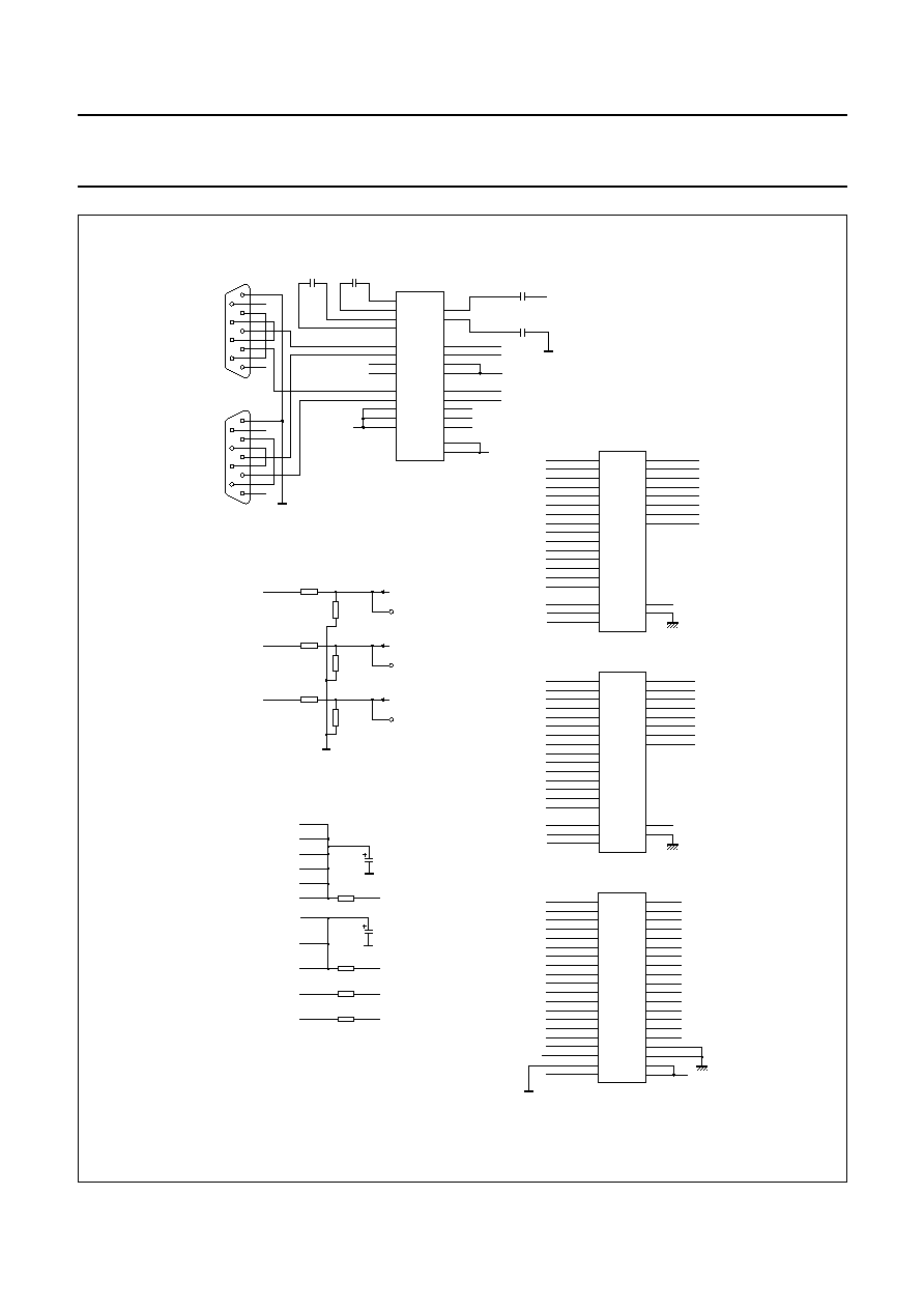
1999 Jun 04
37
Philips Semiconductors
Product specification
Global Positioning System (GPS)
baseband processor
SAA1575HL
Fig.24 Baseband circuitry (continued from Fig.23).
MHB291
handbook, full pagewidth
R224
220
R210
open
R223
220
R209
open
R222
220
R208
open
RFLE
RFCLK
RFDATA
RFLE
RFCLK
RFDATA
RFL
RFC
RFD
TP227
TP226
TP228
GND
VCC1
VCC
VCC2
VCC3
VCC4
VCC5
VCC6
C225
47
µ
F
(6.3 V)
1
R216
VDD1
VDD
VDD2
VDD3
VRTC1
VBB1
C226
47
µ
F
(6.3 V)
1
R213
VRTC
1
R212
VBB
1
R211
GND
GND
11
13
15
16
17
12
18
19
10
8
7
6
5
9
4
3
D4
D5
D6
D7
D0
D1
D2
D3
D12
D13
D14
D15
D8
D9
D10
D11
A5
A6
A7
A8
A1
A2
A3
A4
A4
A5
A6
A7
A0
A1
A2
A3
25
21
23
2
26
24
1
20
A13
A14
A15
/DMCS
A9
A10
A11
A12
A12
A13
A14
/CE
A8
A9
A10
A11
22
/RD
/OE
28
VBB
14
GND
27
/WRH
/WE
U202
M5M5256BVP
11
13
15
16
17
12
18
19
10
8
7
6
5
9
4
3
D4
D5
D6
D7
D0
D1
D2
D3
D4
D5
D6
D7
D0
D1
D2
D3
A5
A6
A7
A8
A1
A2
A3
A4
A4
A5
A6
A7
A0
A1
A2
A3
25
21
23
2
26
24
1
20
A13
A14
A15
/DMCS
A9
A10
A11
A12
A12
A13
A14
/CE
A8
A9
A10
A11
22
/RD
/OE
27
/WRL
/WE
U203
M5M5256BVP
21
19
18
17
16
20
15
14
24
26
27
28
29
25
30
31
D4
D5
D6
D7
D0
D1
D2
D3
11
9
8
7
6
10
5
4
D13
D14
D15
D16
D8
D9
D11
D12
2
43
VPP
VCC
VCC
/PGM
A5
A6
A7
A8
A1
A2
A3
A4
A4
A5
A6
A7
A0
A1
A2
A3
32
36
37
38
39
35
40
A13
A14
A15
A9
A10
A11
A12
A12
A13
A14
A8
A9
A10
A11
41
42
44
A16
A17
A15
A16
3
/CE
22
/PMCS
/OE
U205
27C202
GND
13
7
6
20
21
17
8
5
12
15
16
2
3
14
1
28
/T3IN
/T4IN
R1OUT
R2OUT
V
+
V
-
/T1IN
/T2IN
RXD0
RXD1
TXD0
TXD1
26
22
19
24
25
R4OUT
R5OUT
EN
/SHDN
R3OUT
T1OUT
T2OUT
T3OUT
T4OUT
C1
+
C1
-
C2
+
C2
-
9
27
23
18
4
/R5IN
/R1IN
/R2IN
/R3IN
/R4IN
U201
J201
DB9
DB9
J202
MAX213EAI
VCC
VCC
VCC
VCC
3
7
2
6
1
5
9
4
8
3
7
2
6
1
5
9
4
8
C203
100 nF
(50 V)
C204
100 nF
(50 V)
100 nF
(50 V)
100 nF
(50 V)
C202
C201
GND
GND
28
VBB
14
GND
12
34
GND

1999 Jun 04
38
Philips Semiconductors
Product specification
Global Positioning System (GPS)
baseband processor
SAA1575HL
Fig.25 RF front-end circuit (continued in Fig.26).
MHB292
handbook, full pagewidth
R315
2.7 k
R314
2.7 k
R313
6.8 k
R320
2.21 k
R321
2.21 k
C346
33 nF
C333
33 nF
VCC
VCCA
C344
10 nF
(50 V)
C339
4.7 pF
C340
150 pF
C341
3.9 nF
C342
4700 pF
C337
33 nF
C336
33 nF
C335
33 nF
C338
15 pF
C348
10 pF
C343
4700 pF
VRF
VRF
VRF
VRF
L305
6.8 nH
R326
10 k
R327
10 k
R319
20 k
R316
10 k
R312
3.9 k
R318
10 k
R317
10 k
5
4 5
6
7
8
1
2
3
8
39
12
10
32
40
7
8
1
4
6
X301
TCO-987Q
-
+
2
1
3
D301
SMV1233-004
RFDATA
7
RFCLK
23
RFLE
34
SIGN
R310
18
R311
18
37
30
29
28
27
C334
33 nF
R309
open
R325
1
C347
open
C330
33 nF
1
36
31
33
C332
33 nF
C329
33 nF
19
16
C331
33 nF
9
41
43
SCLK
LIMINN
BFCN
VCCA(LNA1)
VCCA(LNA2)
VCCA(PLL)
VCCA(LIM)
VCCA(MX2)
VCCA(MX1P)
VCCA(VCO)
P41GND
VDDD
LIMINP
SCLK
BFCP
REFIN
P39GND
COMP
P12GND
TANK
DATA
CLOCK
STROBE
SIGN
VRF
VDDD
VCCD
RCLK
U302
MAX903ESA
DGND AGND
AGND
AGND
AGND
AGND
AGND
DGND
AGND
R322
R324
open
12 k
C345
1
µ
F
(16 V)
C308
open
VRF
M1BIASP
M1BIASN
L306
180 nH
L307
180 nH
R323
R304
0
2.21 k
VRF
M2BIASP
M2BIASN
L308
27
µ
H
L309
open
AGND
AGND
AGND
AGND
AGND
AGND
AGND
AGND
UAA1570HL
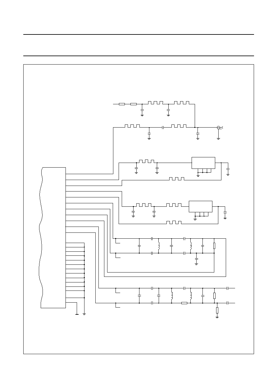
1999 Jun 04
39
Philips Semiconductors
Product specification
Global Positioning System (GPS)
baseband processor
SAA1575HL
Fig.26 RF front-end circuit (continued from Fig.25).
MHB293
handbook, full pagewidth
R306
909
R303
9
R307
9
C315
6.8 pF
C316
6.8 pF
C317
8.2 pF
C318
8.2 pF
C325
27 pF
C328
33 nF
(50 V)
C327
10 pF
(50 V)
C324
1.5 pF
C326
0.56 pF
L303
330 nH
L304
330 nH
45
LNA1IN
48
3
LNA1OUT
LNA2IN
LNA2OUT
UAA1570HL
VRF
L = 367 mils (9.3 mm)
W = 33 mils
50
W = 6 mils 100
C321
0.27 pF
C307
open
C305
open
C323
2.2 pF
L = 355 mils (9 mm)
W = 6 mils
100
L = 286 mils (7.3 mm)
W = 6 mils 100
L = 386 mils (10 mm)
L = 1020 mils
W = 8.8 mils
L = 900 mils
W = 8.8 mils
L = 315 mils (8.1 mm)
W = 6 mils
100
J301
SMA-F
1
2
5
3
4
6
BPF301
MF1012S-1
I/O
I/O
6
14
MX1IN
17
IF1P
M1BIASP
18
IF1N
21
IF2INN
22
IF2INP
24
IF2P
25
IF2N
LIMINP
LIMINN
M1BIASN
M2BIASP
M2BIASN
C320
1.2 pF
C313
36 pF
C314
36 pF
C319
39 pF
R305
820
R302
0
0
R301
C302
47 pF
C304
open
C303
47 pF
C312
1000 pF
C311
1000 pF
L301
22
µ
H
L302
22
µ
H
44
LNA1GND1
46
BIASGND1
47
LNA1GND2
5
LNA2GND2
4
BIASGND2
2
LNA2GND1
42
P42GND
38
PLLGND
26
LIMGND
20
MX2GND
13
MXPGND
35
DGND
15
MX1GND
11
VCOGND
C301
82 pF
C309
18 pF
C310
68 pF
C306
0.47 pF
C322
2.2 pF
L = 412 mils (10.5 mm)
W = 6 mils
100
L = 217 mils (5.5 mm)
W = 33 mils
50
1
2
5
3
4
6
BPF302
MF1012S-1
I/O
I/O
DGND AGND
AGND
AGND
AGND
AGND
AGND
AGND
AGND
AGND
AGND
AGND
AGND
AGND
AGND
AGND
AGND
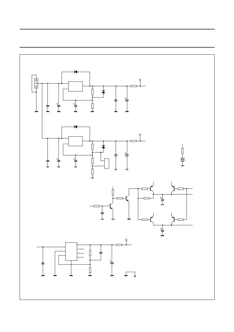
1999 Jun 04
40
Philips Semiconductors
Product specification
Global Positioning System (GPS)
baseband processor
SAA1575HL
Fig.27 Power supply circuitry.
handbook, full pagewidth
MHB294
GND
VBAT
R117
1 k
B101
3 V
170 mAh
C114
22
µ
F
(6.3 V)
V103
BC858
V105
BC858
GND
GND
VCC
VCC
VBAT
R113
47 k
R109
470
R110
1 M
R112
1 M
R115
10 M
BATT_ON
BATT_OFF
VBB
C113
22
µ
F
(6.3 V)
V104
BC858
V102
BC848
V101
BC848
V106
BC858
GND
GND
VDD
VBAT
R114
47 k
R116
10 M
VRTC
R111
1 M
C112
470 nF
GND
U103
LP2951CM
IN
8
SD
3
6
VTAP
2
SNSE
1
OUT
FB
7
4
C105
100 nF
TP103
VDD(IN)
VDD
VCC
C106
100 nF
C111
10
µ
F
(6.3 V)
R106
18 k
R108
12 k
R103
1
GND
GND
GND
GND
GND
GND
GND
5
ERR
U101
PL101
JMP3
IN
2
OUT
3
ADJ
1
C101
1 nF
D102
LL4007
TP101
VCC
VCC
D101
LL4007
C109
10
µ
F
(10 V)
C107
1
µ
F
(20 V)
C102
1 nF
C108
22
µ
F
(5 V)
R118
270
R119
820
R101
1
GND
GND
GND
GND
GND
GND
GND
U102
LM317T(3)
LM317T(3)
IN
2
OUT
3
ADJ
1
3 V/5 V
JP101
1
2
C103
1 nF
D104
LL4007
TP102
VRF
VRF
D103
LL4007
C116
10
µ
F
(10 V)
C115
1
µ
F
(20 V)
C104
1 nF
C110
22
µ
F
(5 V)
R120
240
R121
390
R122
330
R102
1
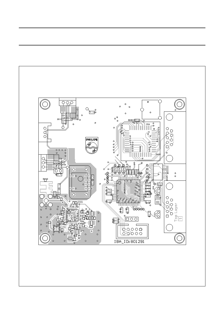
1999 Jun 04
41
Philips Semiconductors
Product specification
Global Positioning System (GPS)
baseband processor
SAA1575HL
The GPS system application demonstration board consists of 6 layers with a total final thickness of 1.5 mm. The PCB
material is FR4.
Fig.28 Demonstration board top layer plus components (real size 88.9 mm
×
88.9 mm).
MHB295
handbook, full pagewidth
C326
BPF302
L303
*
*
D301
L304
R314
R316
R325
R309
R306
R319
R310
R311
R305
R301
C310
C303
R216
C220
R211
C213
R302
L305
L302
L301
C322
C311
C312
C301
U301
C325
C324
C314
C317
C305
C319 C302
C309
C341
JP202
C318
C334
C320
C338
C306
C327
C328
C329
PMCS
WRH
C217
DMCS
PWRFAIL
C211
WRL
RD
PWRDN
PTEST
VRF IN
X301
RS232 #0
U204
C216
C213
C219
C215
C210
R206
PL101
C103
R120
R121
R102
C101
C107
C109
U101
R103
U102 C116
C115
R122
R303
R307
1
BATT_OFF U201
R326
R327
U206
C209
R212
C212
GND/VCC
VCC IN
VDD IN
R118
+
+
R119
C102
R101
JP101
1
BATT_ON
RXD1
TXD1
TXD0
RXD0
RFCLK
RFDATA
RFLE
SIGN
DAC
RCLK
SCLK
T1S_OUT
1
C223
U205
3 V/170 mAh
R205
U207
R224
R210
R223
R209
R222
R208
R213
C214
RS232 #1
GPS DEMO BOARD
Version 1.3

1999 Jun 04
42
Philips Semiconductors
Product specification
Global Positioning System (GPS)
baseband processor
SAA1575HL
Fig.29 Demonstration board 2nd layer.
MHB296
handbook, full pagewidth

1999 Jun 04
43
Philips Semiconductors
Product specification
Global Positioning System (GPS)
baseband processor
SAA1575HL
Fig.30 Demonstration board 3rd layer.
MHB297
handbook, full pagewidth
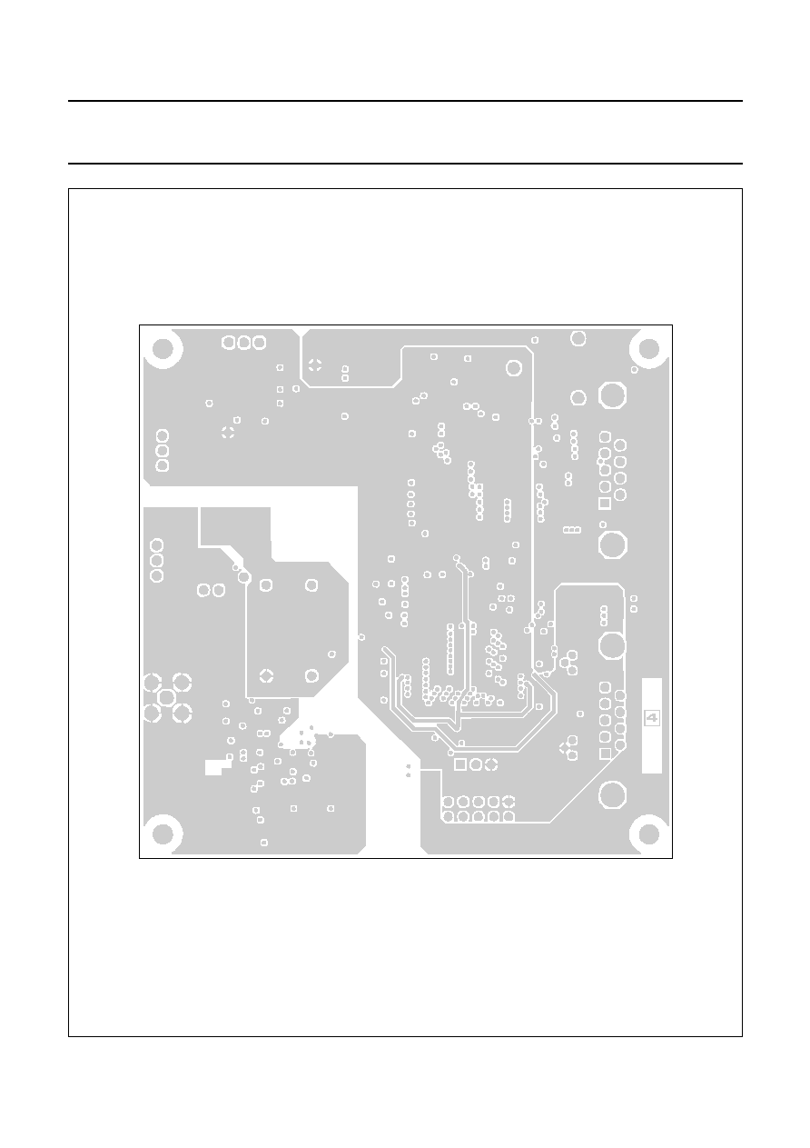
1999 Jun 04
44
Philips Semiconductors
Product specification
Global Positioning System (GPS)
baseband processor
SAA1575HL
Fig.31 Demonstration board 4th layer.
MHB298
handbook, full pagewidth
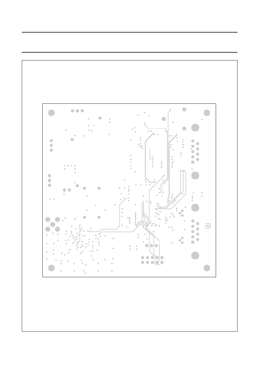
1999 Jun 04
45
Philips Semiconductors
Product specification
Global Positioning System (GPS)
baseband processor
SAA1575HL
Fig.32 Demonstration board 5th layer.
MHB299
handbook, full pagewidth
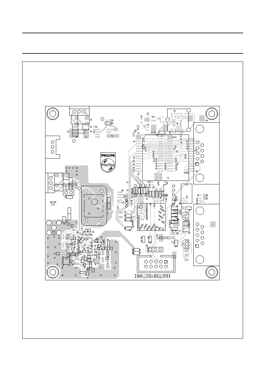
1999 Jun 04
46
Philips Semiconductors
Product specification
Global Positioning System (GPS)
baseband processor
SAA1575HL
Fig.33 Demonstration board bottom layer plus components.
MHB300
handbook, full pagewidth
C326
BPF302
L303
*
*
D301
L304
R314
R316
R325
R309
R306
R319
R310
R311
R305
R301
C310
C303
R216
C220
R211
C213
R302
L305
L302
L301
C322
C311
C312
C301
U301
C325
C324
C314
C317
C305
C319 C302
C309
C341
JP202
C318
C334
C320
C338
C306
C327
C328
C329
PMCS
WRH
C217
DMCS
PWRFAIL
C211
WRL
RD
PWRDN
PTEST
VRF IN
X301
RS232 #0
U204
C216
C213
C219
C215
C210
R206
PL101
C103
R120
R121
R102
C101
C107
C109
U101
R103
U102 C116
C115
R122
R303
R307
1
BATT_OFF U201
R326
R327
U206
C209
R212
C212
GND/VCC
VCC IN
VDD IN
R118
+
+
R119
C102
R101
JP101
1
BATT_ON
RXD1
TXD1
TXD0
RXD0
RFCLK
RFDATA
RFLE
SIGN
DAC
RCLK
SCLK
T1S_OUT
1
C223
U205
3 V/170 mAh
R205
U207
R224
R210
R223
R209
R222
R208
R213
C214
RS232 #1
GPS DEMO BOARD
Version 1.3

1999 Jun 04
47
Philips Semiconductors
Product specification
Global Positioning System (GPS)
baseband processor
SAA1575HL
Table 5
Component list for GPS demonstration board
COMPONENT
TYPE
COMPONENT CHARACTERISTICS
VALUE
TOLERANCE
PACKAGE
B101
Lithium battery
3 V/170 mAh
-
CR1/3
C101 to C104, C311 and C312
ceramic capacitor
1 nF/50 V
10%
603
C105, C106, C201 to C204
ceramic capacitor
100 nF/50 V
20%
603
C107 and C115
ceramic capacitor
1
µ
F/63 V
20%
1210
C108 and C110
tantalum capacitor
22
µ
F/16 V
20%
-
C109 and C116
tantalum capacitor
10
µ
F/16 V
20%
-
C111 and C209
tantalum capacitor
10
µ
F/6.3 V
20%
-
C112
ceramic capacitor
470 nF/63 V
20%
1206
C113 and C114
tantalum capacitor
22
µ
F/6.3 V
20%
-
C205, C206 and C325
ceramic capacitor
27 pF/50 V
5%
603
C207, C208, C327 and C348
ceramic capacitor
10 pF/50 V
5%
603
C210 to C224, C328 to C337 and C346
ceramic capacitor
33 nF/63 V
10%
603
C225 and C226
tantalum capacitor
47
µ
F/6.3 V
20%
-
C301
ceramic capacitor
82 pF/50 V
5%
603
C302 and C303
ceramic capacitor
47 pF/50 V
5%
603
C304, C305, C307, C308 and C347
-
not loaded
-
-
C306
ceramic capacitor
0.47 pF/50 V
±
0.1 pF
603
C309
ceramic capacitor
18 pF/50 V
5%
603
C310
ceramic capacitor
68 pF/50 V
5%
603
C313 and C314
ceramic capacitor
36 pF/50 V
5%
603
C315 and C316
ceramic capacitor
6.8 pF/50 V
±
0.25 pF
603
C317 and C318
ceramic capacitor
8.2 pF/50 V
±
0.25 pF
603
C319
ceramic capacitor
39 pF/50 V
5%
603
C320
ceramic capacitor
1.2 pF/50 V
±
0.25 pF
603
C321
ceramic capacitor
0.27 pF/50 V
±
0.1 pF
603
C322 and C323
ceramic capacitor
2.2 pF/50 V
±
0.25 pF
603
C324
ceramic capacitor
1.5 pF/50 V
±
0.25 pF
603
C326
ceramic capacitor
0.56 pF/50 V
±
0.1 pF
603
C338
ceramic capacitor
15 pF/50 V
5%
603
C339
ceramic capacitor
4.7 pF/50 V
±
0.25 pF
603
C340
ceramic capacitor
150 pF/50 V
5%
603
C341
ceramic capacitor
3.9 nF/50 V
10%
603
C342 and C343
ceramic capacitor
4.7 nF/50 V
5%
603
C344
ceramic capacitor
10 nF/50 V
10%
603
C345
tantalum capacitor
1
µ
F/16 V
20%
-
D101 to D104
LL4007 diode,
equivalent to 1N4007
-
-
-
D201
SMD diode BAS 16
-
-
SOT23

1999 Jun 04
48
Philips Semiconductors
Product specification
Global Positioning System (GPS)
baseband processor
SAA1575HL
D301
Alpha SMV1204-133
varactor
-
-
SOT23
L301 and L302
SMD inductor
22
µ
H
5%
1008
L303 and L304
SMD inductor
330 nH
5%
1008
L305
SMD inductor
6.8 nH
±
5%
603
L306 and L307
SMD inductor
180 nH
±
5%
1008
L308
SMD inductor
27
µ
H
5%
1008
L309
-
not loaded
-
-
R101, R102, R103, R211, R212, R213,
R216 and R325
SMD resistor
1
5%
603
R106
SMD resistor
18 k
5%
603
R108 and R322
SMD resistor
12 k
1%
603
R109 and R207
SMD resistor
470
1%
603
R110, R111, R112 and R204
SMD resistor
1 M
1%
603
R113 and R114
SMD resistor
47 k
1%
603
R115, R116 and R202
SMD resistor
10 M
1%
603
R117
SMD resistor
1 k
1%
603
R118
SMD resistor
270
1%
603
R119 and R305
SMD resistor
820
1%
603
R120
SMD resistor
240
1%
603
R121
SMD resistor
390
1%
603
R122
SMD resistor
330
1%
603
R201, R301, R302 and R304
SMD resistor
0
-
603
R203
SMD resistor
180
5%
603
R205, R206, R316, R317, R318,
R326 and R327
SMD resistor
10 k
1%
603
R208, R209, R210, R309 and R324
-
not loaded
-
-
R222 to R224
SMD resistor
220
5%
603
R303 and R307
SMD resistor
9.1
5%
603
R306
SMD resistor
910
1%
603
R310 and R311
SMD resistor
18
1%
603
R312
SMD resistor
3.9 k
1%
603
R313
SMD resistor
6.8 k
1%
603
R314 and R315
SMD resistor
2.7 k
1%
603
R319
SMD resistor
20 k
5%
603
R320, R321 and R323
SMD resistor
2.2 k
1%
603
U101 and U102
(1)
LM317T voltage
regulator
-
-
TO220
U103
LP2951CM voltage
regulator (National)
-
-
SO8
COMPONENT
TYPE
COMPONENT CHARACTERISTICS
VALUE
TOLERANCE
PACKAGE

1999 Jun 04
49
Philips Semiconductors
Product specification
Global Positioning System (GPS)
baseband processor
SAA1575HL
Note
1. With heat sink depending on input voltage.
U201
MAX213EAIRS2312
transceiver (Maxim)
-
-
SSOP28
U202 and U203
SRAM
M5M5256BFP-70LL
32k
×
8 (Mitsubishi)
-
-
SO28
U205
27C202 EPROM
-
-
PLCC44
U206
ZM33064 power monitor
-
-
-
U207
ZM33164 power monitor
-
-
-
U302
MAX903ESA
comparator (Maxim)
-
-
SO8
V101 and V102
BC848 or BC847C
NPN transistor
-
-
SOT23
V103 to V106
BC858 PNP transistor
-
-
SOT23
X301
TCXO TCO-987Q
-
-
-
Y201
30 MHz crystal,
16 pF load capacitance
-
-
-
Y202
SMD crystal
32.768 kHz
±
30 ppm
-
BPF301 and BPF302
MF1012S-1 saw filter
-
-
-
COMPONENT
TYPE
COMPONENT CHARACTERISTICS
VALUE
TOLERANCE
PACKAGE
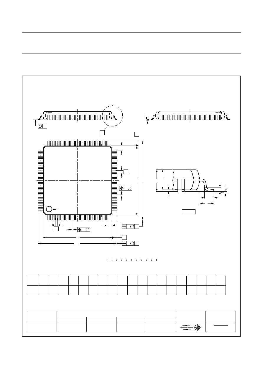
1999 Jun 04
50
Philips Semiconductors
Product specification
Global Positioning System (GPS)
baseband processor
SAA1575HL
13 PACKAGE OUTLINE
UNIT
A
max.
A
1
A
2
A
3
b
p
c
E
(1)
e
H
E
L
L
p
Z
y
w
v
REFERENCES
OUTLINE
VERSION
EUROPEAN
PROJECTION
ISSUE DATE
IEC
JEDEC
EIAJ
mm
1.6
0.20
0.05
1.5
1.3
0.25
0.28
0.16
0.18
0.12
14.1
13.9
0.5
16.25
15.75
1.15
0.85
7
0
o
o
0.12
0.1
0.2
1.0
DIMENSIONS (mm are the original dimensions)
Note
1. Plastic or metal protrusions of 0.25 mm maximum per side are not included.
0.75
0.45
SOT407-1
95-12-19
97-08-04
D
(1)
(1)
(1)
14.1
13.9
H
D
16.25
15.75
E
Z
1.15
0.85
D
b
p
e
E
A
1
A
L
p
detail X
L
(A )
3
B
25
c
D
H
b
p
E
H
A
2
v
M
B
D
ZD
A
Z E
e
v
M
A
X
1
100
76
75
51
50
26
y
pin 1 index
w
M
w
M
0
5
10 mm
scale
LQFP100: plastic low profile quad flat package; 100 leads; body 14 x 14 x 1.4 mm
SOT407-1

1999 Jun 04
51
Philips Semiconductors
Product specification
Global Positioning System (GPS)
baseband processor
SAA1575HL
14 SOLDERING
14.1
Introduction to soldering surface mount
packages
This text gives a very brief insight to a complex technology.
A more in-depth account of soldering ICs can be found in
our
"Data Handbook IC26; Integrated Circuit Packages"
(document order number 9398 652 90011).
There is no soldering method that is ideal for all surface
mount IC packages. Wave soldering is not always suitable
for surface mount ICs, or for printed-circuit boards with
high population densities. In these situations reflow
soldering is often used.
14.2
Reflow soldering
Reflow soldering requires solder paste (a suspension of
fine solder particles, flux and binding agent) to be applied
to the printed-circuit board by screen printing, stencilling or
pressure-syringe dispensing before package placement.
Several methods exist for reflowing; for example,
infrared/convection heating in a conveyor type oven.
Throughput times (preheating, soldering and cooling) vary
between 100 and 200 seconds depending on heating
method.
Typical reflow peak temperatures range from
215 to 250
°
C. The top-surface temperature of the
packages should preferable be kept below 230
°
C.
14.3
Wave soldering
Conventional single wave soldering is not recommended
for surface mount devices (SMDs) or printed-circuit boards
with a high component density, as solder bridging and
non-wetting can present major problems.
To overcome these problems the double-wave soldering
method was specifically developed.
If wave soldering is used the following conditions must be
observed for optimal results:
·
Use a double-wave soldering method comprising a
turbulent wave with high upward pressure followed by a
smooth laminar wave.
·
For packages with leads on two sides and a pitch (e):
larger than or equal to 1.27 mm, the footprint
longitudinal axis is preferred to be parallel to the
transport direction of the printed-circuit board;
smaller than 1.27 mm, the footprint longitudinal axis
must be parallel to the transport direction of the
printed-circuit board.
The footprint must incorporate solder thieves at the
downstream end.
·
For packages with leads on four sides, the footprint must
be placed at a 45
°
angle to the transport direction of the
printed-circuit board. The footprint must incorporate
solder thieves downstream and at the side corners.
During placement and before soldering, the package must
be fixed with a droplet of adhesive. The adhesive can be
applied by screen printing, pin transfer or syringe
dispensing. The package can be soldered after the
adhesive is cured.
Typical dwell time is 4 seconds at 250
°
C.
A mildly-activated flux will eliminate the need for removal
of corrosive residues in most applications.
14.4
Manual soldering
Fix the component by first soldering two
diagonally-opposite end leads. Use a low voltage (24 V or
less) soldering iron applied to the flat part of the lead.
Contact time must be limited to 10 seconds at up to
300
°
C.
When using a dedicated tool, all other leads can be
soldered in one operation within 2 to 5 seconds between
270 and 320
°
C.
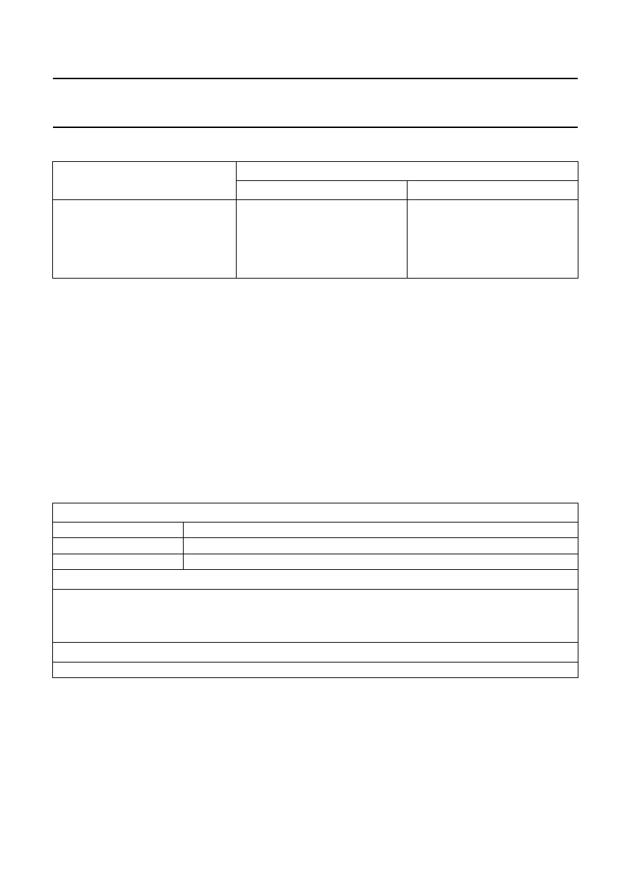
1999 Jun 04
52
Philips Semiconductors
Product specification
Global Positioning System (GPS)
baseband processor
SAA1575HL
14.5
Suitability of surface mount IC packages for wave and reflow soldering methods
Notes
1. All surface mount (SMD) packages are moisture sensitive. Depending upon the moisture content, the maximum
temperature (with respect to time) and body size of the package, there is a risk that internal or external package
cracks may occur due to vaporization of the moisture in them (the so called popcorn effect). For details, refer to the
Drypack information in the
"Data Handbook IC26; Integrated Circuit Packages; Section: Packing Methods".
2. These packages are not suitable for wave soldering as a solder joint between the printed-circuit board and heatsink
(at bottom version) can not be achieved, and as solder may stick to the heatsink (on top version).
3. If wave soldering is considered, then the package must be placed at a 45
°
angle to the solder wave direction.
The package footprint must incorporate solder thieves downstream and at the side corners.
4. Wave soldering is only suitable for LQFP, TQFP and QFP packages with a pitch (e) equal to or larger than 0.8 mm;
it is definitely not suitable for packages with a pitch (e) equal to or smaller than 0.65 mm.
5. Wave soldering is only suitable for SSOP and TSSOP packages with a pitch (e) equal to or larger than 0.65 mm; it is
definitely not suitable for packages with a pitch (e) equal to or smaller than 0.5 mm.
15 DEFINITIONS
16 LIFE SUPPORT APPLICATIONS
These products are not designed for use in life support appliances, devices, or systems where malfunction of these
products can reasonably be expected to result in personal injury. Philips customers using or selling these products for
use in such applications do so at their own risk and agree to fully indemnify Philips for any damages resulting from such
improper use or sale.
PACKAGE
SOLDERING METHOD
WAVE
REFLOW
(1)
BGA, SQFP
not suitable
suitable
HLQFP, HSQFP, HSOP, HTSSOP, SMS not suitable
(2)
suitable
PLCC
(3)
, SO, SOJ
suitable
suitable
LQFP, QFP, TQFP
not recommended
(3)(4)
suitable
SSOP, TSSOP, VSO
not recommended
(5)
suitable
Data sheet status
Objective specification
This data sheet contains target or goal specifications for product development.
Preliminary specification
This data sheet contains preliminary data; supplementary data may be published later.
Product specification
This data sheet contains final product specifications.
Limiting values
Limiting values given are in accordance with the Absolute Maximum Rating System (IEC 134). Stress above one or
more of the limiting values may cause permanent damage to the device. These are stress ratings only and operation
of the device at these or at any other conditions above those given in the Characteristics sections of the specification
is not implied. Exposure to limiting values for extended periods may affect device reliability.
Application information
Where application information is given, it is advisory and does not form part of the specification.

1999 Jun 04
53
Philips Semiconductors
Product specification
Global Positioning System (GPS)
baseband processor
SAA1575HL
NOTES

1999 Jun 04
54
Philips Semiconductors
Product specification
Global Positioning System (GPS)
baseband processor
SAA1575HL
NOTES

1999 Jun 04
55
Philips Semiconductors
Product specification
Global Positioning System (GPS)
baseband processor
SAA1575HL
NOTES

© Philips Electronics N.V.
SCA
All rights are reserved. Reproduction in whole or in part is prohibited without the prior written consent of the copyright owner.
The information presented in this document does not form part of any quotation or contract, is believed to be accurate and reliable and may be changed
without notice. No liability will be accepted by the publisher for any consequence of its use. Publication thereof does not convey nor imply any license
under patent- or other industrial or intellectual property rights.
Internet: http://www.semiconductors.philips.com
1999
65
Philips Semiconductors a worldwide company
Netherlands: Postbus 90050, 5600 PB EINDHOVEN, Bldg. VB,
Tel. +31 40 27 82785, Fax. +31 40 27 88399
New Zealand: 2 Wagener Place, C.P.O. Box 1041, AUCKLAND,
Tel. +64 9 849 4160, Fax. +64 9 849 7811
Norway: Box 1, Manglerud 0612, OSLO,
Tel. +47 22 74 8000, Fax. +47 22 74 8341
Pakistan: see Singapore
Philippines: Philips Semiconductors Philippines Inc.,
106 Valero St. Salcedo Village, P.O. Box 2108 MCC, MAKATI,
Metro MANILA, Tel. +63 2 816 6380, Fax. +63 2 817 3474
Poland: Ul. Lukiska 10, PL 04-123 WARSZAWA,
Tel. +48 22 612 2831, Fax. +48 22 612 2327
Portugal: see Spain
Romania: see Italy
Russia: Philips Russia, Ul. Usatcheva 35A, 119048 MOSCOW,
Tel. +7 095 755 6918, Fax. +7 095 755 6919
Singapore: Lorong 1, Toa Payoh, SINGAPORE 319762,
Tel. +65 350 2538, Fax. +65 251 6500
Slovakia: see Austria
Slovenia: see Italy
South Africa: S.A. PHILIPS Pty Ltd., 195-215 Main Road Martindale,
2092 JOHANNESBURG, P.O. Box 58088 Newville 2114,
Tel. +27 11 471 5401, Fax. +27 11 471 5398
South America: Al. Vicente Pinzon, 173, 6th floor,
04547-130 SĂO PAULO, SP, Brazil,
Tel. +55 11 821 2333, Fax. +55 11 821 2382
Spain: Balmes 22, 08007 BARCELONA,
Tel. +34 93 301 6312, Fax. +34 93 301 4107
Sweden: Kottbygatan 7, Akalla, S-16485 STOCKHOLM,
Tel. +46 8 5985 2000, Fax. +46 8 5985 2745
Switzerland: Allmendstrasse 140, CH-8027 ZÜRICH,
Tel. +41 1 488 2741 Fax. +41 1 488 3263
Taiwan: Philips Semiconductors, 6F, No. 96, Chien Kuo N. Rd., Sec. 1,
TAIPEI, Taiwan Tel. +886 2 2134 2886, Fax. +886 2 2134 2874
Thailand: PHILIPS ELECTRONICS (THAILAND) Ltd.,
209/2 Sanpavuth-Bangna Road Prakanong, BANGKOK 10260,
Tel. +66 2 745 4090, Fax. +66 2 398 0793
Turkey: Yukari Dudullu, Org. San. Blg., 2.Cad. Nr. 28 81260 Umraniye,
ISTANBUL, Tel. +90 216 522 1500, Fax. +90 216 522 1813
Ukraine: PHILIPS UKRAINE, 4 Patrice Lumumba str., Building B, Floor 7,
252042 KIEV, Tel. +380 44 264 2776, Fax. +380 44 268 0461
United Kingdom: Philips Semiconductors Ltd., 276 Bath Road, Hayes,
MIDDLESEX UB3 5BX, Tel. +44 181 730 5000, Fax. +44 181 754 8421
United States: 811 East Arques Avenue, SUNNYVALE, CA 94088-3409,
Tel. +1 800 234 7381, Fax. +1 800 943 0087
Uruguay: see South America
Vietnam: see Singapore
Yugoslavia: PHILIPS, Trg N. Pasica 5/v, 11000 BEOGRAD,
Tel. +381 11 62 5344, Fax.+381 11 63 5777
For all other countries apply to: Philips Semiconductors,
International Marketing & Sales Communications, Building BE-p, P.O. Box 218,
5600 MD EINDHOVEN, The Netherlands, Fax. +31 40 27 24825
Argentina: see South America
Australia: 34 Waterloo Road, NORTH RYDE, NSW 2113,
Tel. +61 2 9805 4455, Fax. +61 2 9805 4466
Austria: Computerstr. 6, A-1101 WIEN, P.O. Box 213,
Tel. +43 1 60 101 1248, Fax. +43 1 60 101 1210
Belarus: Hotel Minsk Business Center, Bld. 3, r. 1211, Volodarski Str. 6,
220050 MINSK, Tel. +375 172 20 0733, Fax. +375 172 20 0773
Belgium: see The Netherlands
Brazil: see South America
Bulgaria: Philips Bulgaria Ltd., Energoproject, 15th floor,
51 James Bourchier Blvd., 1407 SOFIA,
Tel. +359 2 68 9211, Fax. +359 2 68 9102
Canada: PHILIPS SEMICONDUCTORS/COMPONENTS,
Tel. +1 800 234 7381, Fax. +1 800 943 0087
China/Hong Kong: 501 Hong Kong Industrial Technology Centre,
72 Tat Chee Avenue, Kowloon Tong, HONG KONG,
Tel. +852 2319 7888, Fax. +852 2319 7700
Colombia: see South America
Czech Republic: see Austria
Denmark: Sydhavnsgade 23, 1780 COPENHAGEN V,
Tel. +45 33 29 3333, Fax. +45 33 29 3905
Finland: Sinikalliontie 3, FIN-02630 ESPOO,
Tel. +358 9 615 800, Fax. +358 9 6158 0920
France: 51 Rue Carnot, BP317, 92156 SURESNES Cedex,
Tel. +33 1 4099 6161, Fax. +33 1 4099 6427
Germany: Hammerbrookstraße 69, D-20097 HAMBURG,
Tel. +49 40 2353 60, Fax. +49 40 2353 6300
Hungary: see Austria
India: Philips INDIA Ltd, Band Box Building, 2nd floor,
254-D, Dr. Annie Besant Road, Worli, MUMBAI 400 025,
Tel. +91 22 493 8541, Fax. +91 22 493 0966
Indonesia: PT Philips Development Corporation, Semiconductors Division,
Gedung Philips, Jl. Buncit Raya Kav.99-100, JAKARTA 12510,
Tel. +62 21 794 0040 ext. 2501, Fax. +62 21 794 0080
Ireland: Newstead, Clonskeagh, DUBLIN 14,
Tel. +353 1 7640 000, Fax. +353 1 7640 200
Israel: RAPAC Electronics, 7 Kehilat Saloniki St, PO Box 18053,
TEL AVIV 61180, Tel. +972 3 645 0444, Fax. +972 3 649 1007
Italy: PHILIPS SEMICONDUCTORS, Piazza IV Novembre 3,
20124 MILANO, Tel. +39 02 67 52 2531, Fax. +39 02 67 52 2557
Japan: Philips Bldg 13-37, Kohnan 2-chome, Minato-ku,
TOKYO 108-8507, Tel. +81 3 3740 5130, Fax. +81 3 3740 5057
Korea: Philips House, 260-199 Itaewon-dong, Yongsan-ku, SEOUL,
Tel. +82 2 709 1412, Fax. +82 2 709 1415
Malaysia: No. 76 Jalan Universiti, 46200 PETALING JAYA, SELANGOR,
Tel. +60 3 750 5214, Fax. +60 3 757 4880
Mexico: 5900 Gateway East, Suite 200, EL PASO, TEXAS 79905,
Tel. +9-5 800 234 7381, Fax +9-5 800 943 0087
Middle East: see Italy
Printed in The Netherlands
285002/02/pp56
Date of release: 1999 Jun 04
Document order number:
9397 750 06055