
PTN3331
High speed differential line driver
Rev. 01 -- 06 August 2002
Product data
1.
Description
The PTN3331 is a differential line driver that implements the electrical characteristics
of Low-Voltage Differential Signaling (LVDS) that meets or exceeds the requirements
of the ANSI
TIA/EIA-644 Standard. LVDS is used to achieve higher data rates on
commonly used media. LVDS overcomes the limitations of achievable slew rates and
EMI restrictions of previous differential signaling techniques. The PTN3331 operates
at 3.3 volt supply levels and current mode output drivers. The output drivers will
deliver a minimum of 247 mV into a 100
load when enabled.
The intended application of this device is for point-to-point baseband transmission
rates over a controlled impedance media of approximately 100
. The maximum rate
and distance of data transfer is dependent upon the attenuation characteristics of the
media selected and the noise coupling to the environment.
The PTN3331 is designed to function over the full industrial temperature range of
-
40
�
C to +85
�
C.
2.
Features
s
Meets or exceeds the requirements of ANSI
TIA/EIA-644 Standard
s
Low-Voltage Differential Signaling with output voltage of 350 mV across a 100
load
s
300 ps maximum channel to channel output skew
s
500 ps typical output voltage rise and fall times
s
Power dissipation of 100 mW typical at 200 MHz
s
Driver at high impedance when disabled or with V
CC
= 0 V
s
5 volt tolerant inputs with Low Voltage TTL (LVTTL) logic input levels
s
Pin-compatible with AM26LS31 and SN65LVDS31.
3.
Applications
s
Low voltage, low EMI, high speed differential signaling
s
Point-to-point high speed data transmission
s
High performance switches and routers.

Philips Semiconductors
PTN3331
High speed differential line driver
Product data
Rev. 01 -- 06 August 2002
2 of 14
9397 750 08339
� Koninklijke Philips Electronics N.V. 2002. All rights reserved.
4.
Ordering information
5.
Functional diagram
Table 1:
Ordering information
Type number
Package
Name
Description
Version
PTN3331DH
TSSOP16
plastic thin shrink small outline package; 16 leads; body width 4.4 mm
SOT403-1
PTN3331D
SO16
plastic small outline package; 16 leads; body width 3.9 mm
SOT109-1
Fig 1.
Functional diagram.
002aaa017
PTN3331
1Y
1Z
2Y
2Z
3Y
3Z
4Y
4Z
G
G
1A
2A
3A
4A
LVDS
LVDS
LVDS
LVDS
4
12
1
7
9
15
2
3
6
5
10
11
14
13
Philips Semiconductors
PTN3331
High speed differential line driver
Product data
Rev. 01 -- 06 August 2002
3 of 14
9397 750 08339
� Koninklijke Philips Electronics N.V. 2002. All rights reserved.
6.
Pinning information
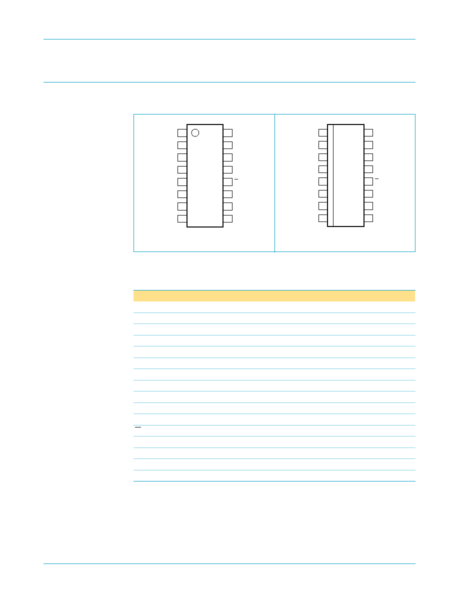
6.1 Pinning
6.2 Pin description
Fig 2.
TSSOP16 pin configuration.
Fig 3.
SO16 pin configuration.
PTN3331DH
002aaa025
1
2
3
4
5
6
7
8
1A
1Y
1Z
G
2Z
2Y
2A
GND
V
CC
4A
4Y
4Z
G
3Z
3Y
3A
16
15
14
13
12
11
10
9
PTN3331D
002aaa018
1
2
3
4
5
6
7
8
1A
1Y
1Z
G
2Z
2Y
2A
GND
V
CC
4A
4Y
4Z
G
3Z
3Y
3A
16
15
14
13
12
11
10
9
Table 2:
Pin description
Symbol
Pin
Description
1A
1
LVTTL input
1Y
2
LVDS non-inverting output
1Z
3
LVDS inverting output
G
4
Enable (active-HIGH)
2Z
5
LVDS inverting output
2Y
6
LVDS non-inverting output
2A
7
LVTTL input
GND
8
Ground
3A
9
LVTTL input
3Y
10
LVDS non-inverting output
3Z
11
LVDS inverting output
G
12
Enable (active-LOW)
4Z
13
LVDS inverting output
4Y
14
LVDS non-inverting output
4A
15
LVTTL input
V
CC
16
Supply

Philips Semiconductors
PTN3331
High speed differential line driver
Product data
Rev. 01 -- 06 August 2002
4 of 14
9397 750 08339
� Koninklijke Philips Electronics N.V. 2002. All rights reserved.
7.
Functional description
7.1 Function table
8.
Limiting values
[1]
Values beyond absolute maximum ratings can cause the device to be prematurely damaged.
Absolute maximum ratings are stress ratings only and functional device operation is not implied.
9.
Recommended operating conditions
Table 3:
Function table
H = HIGH level; L = LOW level; X = irrelevant; Z = high impedance.
Input
Enables
Outputs
A
G
G
Y
Z
H
H
X
H
L
L
H
X
L
H
H
X
L
H
L
L
X
L
L
H
X
L
H
Z
Z
Open
H
X
L
H
Open
X
L
L
H
Table 4:
Limiting values
In accordance with the Absolute Maximum Rating System (IEC 60134).
Symbol
Parameter
Min
Max
Unit
V
CC
supply voltage
-
0.5
4.0
V
V
I
input voltage
-
0.5
V
CC
+ 0.5
V
short circuit duration
Continuous
sec
T
amb
operating ambient temperature range
-
40
+85
�
C
T
j
operating junction temperature
-
40
+150
�
C
T
stg
storage temperature range
-
65
+150
�
C
ESD
>2
-
kV
Table 5:
Recommended operating conditions
Symbol
Parameter
Min
Nom
Max
Unit
V
CC
supply voltage
3
3.3
3.6
V
V
IH
HIGH-level input voltage
2
-
-
V
V
IL
LOW-level input voltage
-
-
0.8
V

Philips Semiconductors
PTN3331
High speed differential line driver
Product data
Rev. 01 -- 06 August 2002
5 of 14
9397 750 08339
� Koninklijke Philips Electronics N.V. 2002. All rights reserved.
10. Static characteristics
[1]
All typical values are at T
amb
= 25
�
C and V
CC
= 3.3 V.
Table 6:
DC electrical characteristics
Over recommended operating conditions, unless otherwise noted.
Symbol
Parameter
Conditions
Min
Typ
[1]
Max
Unit
V
OD
differential output voltage
R
L
= 100
See
Figure 4
.
247
340
454
mV
V
OD
change in differential voltage
magnitude between logic states
-
50
-
+50
mV
V
OC(SS)
Steady-state common-mode output
voltage
1.125
1.2
1.375
V
V
OC(SS)
Change in steady-state
common-mode output voltage
between logic states
-
50
-
+50
mV
V
OC(PP)
Peak-to-peak common-mode output
voltage
-
50
150
mV
I
CC
Supply current
V
I
= 0.8 or 2 V;
enabled, no load
-
22
30
mA
V
I
= 0.8 or 2 V;
enabled, R
L
= 100
-
25
35
mA
V
I
= 0 V or V
CC
;
disabled
-
0.25
1
mA
I
IH
HIGH-level input current
V
IH
= 2 V
-
4
20
�
A
I
IL
LOW-level input current
V
IL
= 0.8 V
-
0.1
10
�
A
I
OS
Output short circuit current
V
O(Y)
or V
O(Z)
= 0 V
-
-
4
-
24
mA
I
OZ
High-impedance output current
V
OD
= 0 V or 2.4 V
-
�
1
-
�
A
I
O(OFF)
Power-off output current
V
CC
= 0 V; V
O
= 2.4 V
1
-
-
1
�
A
C
i
Input capacitance
-
3
-
pF

Philips Semiconductors
PTN3331
High speed differential line driver
Product data
Rev. 01 -- 06 August 2002
6 of 14
9397 750 08339
� Koninklijke Philips Electronics N.V. 2002. All rights reserved.
11. Dynamic characteristics
[1]
All typical values are at T
amb
= 25
�
C, and V
CC
= 3.3 V.
[2]
t
sk(o)
is the skew between specified outputs of a single device with all driving inputs connected together and the outputs switching in the
same direction while driving identical specified loads.
[3]
t
sk(p-p)
is the magnitude of the difference in propagation delay times between any specified terminals of two devices when both devices
operate with the same supply voltages, same temperature, and have identical packages and test circuits.
[4]
Guaranteed by design and characterization.
Table 7:
AC electrical characteristics
Over recommended operating conditions, unless otherwise noted.
Symbol
Parameter
Conditions
Min
Typ
[1]
Max
Unit
t
PLH
Propagation delay, LOW-to-HIGH level
output
R
L
= 100
;
C
L
= 10 pF
See
Figure 5
.
0.5
1.4
2
ns
t
PHL
Propagation delay, HIGH-to-LOW level
output
1
1.7
2.5
ns
t
r
Differential output rise time (20 to 80%)
[4]
0.4
0.5
0.6
ns
t
f
Differential output fall time (80 to 20%)
[4]
0.4
0.5
0.6
ns
t
sk(p)
Pulse skew (t
PHL
-
t
PLH
)
-
0.3
0.6
ns
t
sk(o)
Channel-to-channel output skew
[2]
,
[4]
-
0
0.3
ns
t
sk(p-p)
Part-to-part skew
[3]
,
[4]
-
-
800
ps
t
PZH
Propagation delay, high-impedance to
HIGH-level output
See
Figure 6
.
-
5.4
15
ns
t
PZL
Propagation delay, high-impedance to
LOW-level output
-
2.5
15
ns
t
PHZ
Propagation delay, HIGH-level to
high-impedance output
-
8.1
15
ns
t
PLZ
Propagation delay, LOW-level to
high-impedance output
-
7.3
15
ns
Philips Semiconductors
PTN3331
High speed differential line driver
Product data
Rev. 01 -- 06 August 2002
7 of 14
9397 750 08339
� Koninklijke Philips Electronics N.V. 2002. All rights reserved.
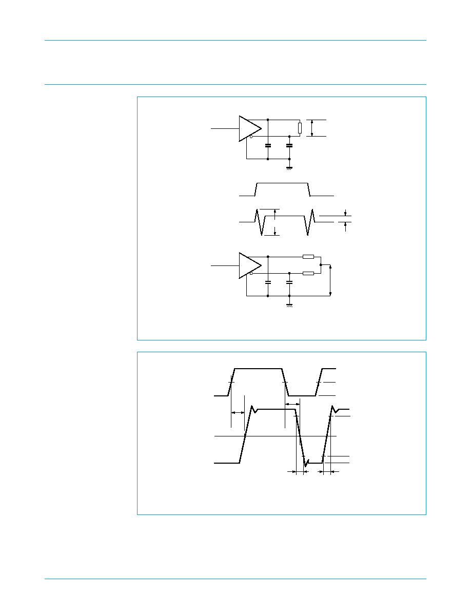
12. Test figures
Fig 4.
Test circuit and voltage definitions.
Fig 5.
Propagation delay definitions.
002aaa019
LVDS
A
Y
Z
C
L
10 pF
C
L
10 pF
R
100
�
1%
A
V
OD
V
OC(PP)
V
OC
V
OC(SS)
LVDS
A
Y
Z
C
L
10 pF
C
L
10 pF
R = 49.9
�
1%
(2 PLACES)
V
OC
002aaa020
2 V
1.4 V
0.8 V
100%
80%
20%
0%
A INPUT
t
PLH
V
OD
t
PHL
t
f
t
r

Philips Semiconductors
PTN3331
High speed differential line driver
Product data
Rev. 01 -- 06 August 2002
8 of 14
9397 750 08339
� Koninklijke Philips Electronics N.V. 2002. All rights reserved.
Fig 6.
Enable and disable time definitions.
002aaa021
t
PZH
t
PZL
2 V
1.4 V
0.8 V
2 V
1.4 V
0.8 V
G
G
100%,
1.4 V
50%
0%, 1.2 V
t
PLZ
t
PHZ
0%,
1 V
50%
100%, 1.2 V
Philips Semiconductors
PTN3331
High speed differential line driver
Product data
Rev. 01 -- 06 August 2002
9 of 14
9397 750 08339
� Koninklijke Philips Electronics N.V. 2002. All rights reserved.
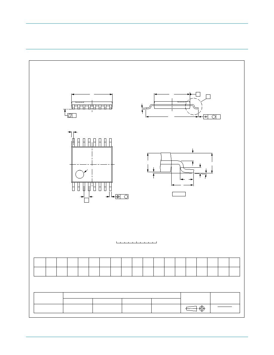
13. Package outline
Fig 7.
TSSOP16 package outline (SOT403-1).
UNIT
A
1
A
2
A
3
b
p
c
D
(1)
E
(2)
(1)
e
H
E
L
L
p
Q
Z
y
w
v
REFERENCES
OUTLINE
VERSION
EUROPEAN
PROJECTION
ISSUE DATE
IEC
JEDEC
EIAJ
mm
0.15
0.05
0.95
0.80
0.30
0.19
0.2
0.1
5.1
4.9
4.5
4.3
0.65
6.6
6.2
0.4
0.3
0.40
0.06
8
0
o
o
0.13
0.1
0.2
1.0
DIMENSIONS (mm are the original dimensions)
Notes
1. Plastic or metal protrusions of 0.15 mm maximum per side are not included.
2. Plastic interlead protrusions of 0.25 mm maximum per side are not included.
0.75
0.50
SOT403-1
MO-153
95-04-04
99-12-27
w
M
b
p
D
Z
e
0.25
1
8
16
9
A
A
1
A
2
L
p
Q
detail X
L
(A )
3
H
E
E
c
v
M
A
X
A
y
0
2.5
5 mm
scale
TSSOP16: plastic thin shrink small outline package; 16 leads; body width 4.4 mm
SOT403-1
A
max.
1.10
pin 1 index

Philips Semiconductors
PTN3331
High speed differential line driver
Product data
Rev. 01 -- 06 August 2002
10 of 14
9397 750 08339
� Koninklijke Philips Electronics N.V. 2002. All rights reserved.
Fig 8.
SO16 package outline (SOT109-1).
X
w
M
A
A
1
A
2
b
p
D
H
E
L
p
Q
detail X
E
Z
e
c
L
v
M
A
(A )
3
A
8
9
1
16
y
pin 1 index
UNIT
A
max.
A
1
A
2
A
3
b
p
c
D
(1)
E
(1)
(1)
e
H
E
L
L
p
Q
Z
y
w
v
REFERENCES
OUTLINE
VERSION
EUROPEAN
PROJECTION
ISSUE DATE
IEC
JEDEC
EIAJ
mm
inches
1.75
0.25
0.10
1.45
1.25
0.25
0.49
0.36
0.25
0.19
10.0
9.8
4.0
3.8
1.27
6.2
5.8
0.7
0.6
0.7
0.3
8
0
o
o
0.25
0.1
DIMENSIONS (inch dimensions are derived from the original mm dimensions)
Note
1. Plastic or metal protrusions of 0.15 mm maximum per side are not included.
1.0
0.4
SOT109-1
97-05-22
99-12-27
076E07
MS-012
0.069
0.010
0.004
0.057
0.049
0.01
0.019
0.014
0.0100
0.0075
0.39
0.38
0.16
0.15
0.050
1.05
0.041
0.244
0.228
0.028
0.020
0.028
0.012
0.01
0.25
0.01
0.004
0.039
0.016
0
2.5
5 mm
scale
SO16: plastic small outline package; 16 leads; body width 3.9 mm
SOT109-1

Philips Semiconductors
PTN3331
High speed differential line driver
Product data
Rev. 01 -- 06 August 2002
11 of 14
9397 750 08339
� Koninklijke Philips Electronics N.V. 2002. All rights reserved.
14. Soldering
14.1 Introduction to soldering surface mount packages
This text gives a very brief insight to a complex technology. A more in-depth account
of soldering ICs can be found in our
Data Handbook IC26; Integrated Circuit
Packages (document order number 9398 652 90011).
There is no soldering method that is ideal for all surface mount IC packages. Wave
soldering can still be used for certain surface mount ICs, but it is not suitable for fine
pitch SMDs. In these situations reflow soldering is recommended.
14.2 Reflow soldering
Reflow soldering requires solder paste (a suspension of fine solder particles, flux and
binding agent) to be applied to the printed-circuit board by screen printing, stencilling
or pressure-syringe dispensing before package placement.
Several methods exist for reflowing; for example, convection or convection/infrared
heating in a conveyor type oven. Throughput times (preheating, soldering and
cooling) vary between 100 and 200 seconds depending on heating method.
Typical reflow peak temperatures range from 215 to 250
�
C. The top-surface
temperature of the packages should preferable be kept below 220
�
C for thick/large
packages, and below 235
�
C small/thin packages.
14.3 Wave soldering
Conventional single wave soldering is not recommended for surface mount devices
(SMDs) or printed-circuit boards with a high component density, as solder bridging
and non-wetting can present major problems.
To overcome these problems the double-wave soldering method was specifically
developed.
If wave soldering is used the following conditions must be observed for optimal
results:
�
Use a double-wave soldering method comprising a turbulent wave with high
upward pressure followed by a smooth laminar wave.
�
For packages with leads on two sides and a pitch (e):
� larger than or equal to 1.27 mm, the footprint longitudinal axis is preferred to be
parallel to the transport direction of the printed-circuit board;
� smaller than 1.27 mm, the footprint longitudinal axis must be parallel to the
transport direction of the printed-circuit board.
The footprint must incorporate solder thieves at the downstream end.
�
For packages with leads on four sides, the footprint must be placed at a 45
�
angle
to the transport direction of the printed-circuit board. The footprint must
incorporate solder thieves downstream and at the side corners.

Philips Semiconductors
PTN3331
High speed differential line driver
Product data
Rev. 01 -- 06 August 2002
12 of 14
9397 750 08339
� Koninklijke Philips Electronics N.V. 2002. All rights reserved.
During placement and before soldering, the package must be fixed with a droplet of
adhesive. The adhesive can be applied by screen printing, pin transfer or syringe
dispensing. The package can be soldered after the adhesive is cured.
Typical dwell time is 4 seconds at 250
�
C. A mildly-activated flux will eliminate the
need for removal of corrosive residues in most applications.
14.4 Manual soldering
Fix the component by first soldering two diagonally-opposite end leads. Use a low
voltage (24 V or less) soldering iron applied to the flat part of the lead. Contact time
must be limited to 10 seconds at up to 300
�
C.
When using a dedicated tool, all other leads can be soldered in one operation within
2 to 5 seconds between 270 and 320
�
C.
14.5 Package related soldering information
[1]
For more detailed information on the BGA packages refer to the
(LF)BGA Application Note
(AN01026); order a copy from your Philips Semiconductors sales office.
[2]
All surface mount (SMD) packages are moisture sensitive. Depending upon the moisture content, the
maximum temperature (with respect to time) and body size of the package, there is a risk that internal
or external package cracks may occur due to vaporization of the moisture in them (the so called
popcorn effect). For details, refer to the Drypack information in the
Data Handbook IC26; Integrated
Circuit Packages; Section: Packing Methods.
[3]
These packages are not suitable for wave soldering. On versions with the heatsink on the bottom
side, the solder cannot penetrate between the printed-circuit board and the heatsink. On versions with
the heatsink on the top side, the solder might be deposited on the heatsink surface.
[4]
If wave soldering is considered, then the package must be placed at a 45
�
angle to the solder wave
direction. The package footprint must incorporate solder thieves downstream and at the side corners.
[5]
Wave soldering is suitable for LQFP, QFP and TQFP packages with a pitch (e) larger than 0.8 mm; it
is definitely not suitable for packages with a pitch (e) equal to or smaller than 0.65 mm.
[6]
Wave soldering is suitable for SSOP and TSSOP packages with a pitch (e) equal to or larger than
0.65 mm; it is definitely not suitable for packages with a pitch (e) equal to or smaller than 0.5 mm.
15. Revision history
Table 8:
Suitability of surface mount IC packages for wave and reflow soldering
methods
Package
[1]
Soldering method
Wave
Reflow
[2]
BGA, LBGA, LFBGA, SQFP, TFBGA, VFBGA
not suitable
suitable
HBCC, HBGA, HLQFP, HSQFP, HSOP,
HTQFP, HTSSOP, HVQFN, HVSON, SMS
not suitable
[3]
suitable
PLCC
[4]
, SO, SOJ
suitable
suitable
LQFP, QFP, TQFP
not recommended
[4][5]
suitable
SSOP, TSSOP, VSO
not recommended
[6]
suitable
Table 9:
Revision history
Rev Date
CPCN
Description
01
20020806
-
Product data. Initial version. Engineering Change Notice 853-2362 28701 dated
2002 August 06.

9397 750 08339
Philips Semiconductors
PTN3331
High speed differential line driver
� Koninklijke Philips Electronics N.V. 2002. All rights reserved.
Product data
Rev. 01 -- 06 August 2002
13 of 14
Contact information
For additional information, please visit http://www.semiconductors.philips.com.
For sales office addresses, send e-mail to: sales.addresses@www.semiconductors.philips.com.
Fax: +31 40 27 24825
16. Data sheet status
[1]
Please consult the most recently issued data sheet before initiating or completing a design.
[2]
The product status of the device(s) described in this data sheet may have changed since this data sheet was published. The latest information is available on the Internet at
URL http://www.semiconductors.philips.com.
17. Definitions
Short-form specification -- The data in a short-form specification is
extracted from a full data sheet with the same type number and title. For
detailed information see the relevant data sheet or data handbook.
Limiting values definition -- Limiting values given are in accordance with
the Absolute Maximum Rating System (IEC 60134). Stress above one or
more of the limiting values may cause permanent damage to the device.
These are stress ratings only and operation of the device at these or at any
other conditions above those given in the Characteristics sections of the
specification is not implied. Exposure to limiting values for extended periods
may affect device reliability.
Application information -- Applications that are described herein for any
of these products are for illustrative purposes only. Philips Semiconductors
make no representation or warranty that such applications will be suitable for
the specified use without further testing or modification.
18. Disclaimers
Life support -- These products are not designed for use in life support
appliances, devices, or systems where malfunction of these products can
reasonably be expected to result in personal injury. Philips Semiconductors
customers using or selling these products for use in such applications do so
at their own risk and agree to fully indemnify Philips Semiconductors for any
damages resulting from such application.
Right to make changes -- Philips Semiconductors reserves the right to
make changes, without notice, in the products, including circuits, standard
cells, and/or software, described or contained herein in order to improve
design and/or performance. Philips Semiconductors assumes no
responsibility or liability for the use of any of these products, conveys no
licence or title under any patent, copyright, or mask work right to these
products, and makes no representations or warranties that these products are
free from patent, copyright, or mask work right infringement, unless otherwise
specified.
Data sheet status
[1]
Product status
[2]
Definition
Objective data
Development
This data sheet contains data from the objective specification for product development. Philips Semiconductors
reserves the right to change the specification in any manner without notice.
Preliminary data
Qualification
This data sheet contains data from the preliminary specification. Supplementary data will be published at a
later date. Philips Semiconductors reserves the right to change the specification without notice, in order to
improve the design and supply the best possible product.
Product data
Production
This data sheet contains data from the product specification. Philips Semiconductors reserves the right to
make changes at any time in order to improve the design, manufacturing and supply. Changes will be
communicated according to the Customer Product/Process Change Notification (CPCN) procedure
SNW-SQ-650A.

� Koninklijke Philips Electronics N.V. 2002.
Printed in the U.S.A
All rights are reserved. Reproduction in whole or in part is prohibited without the prior
written consent of the copyright owner.
The information presented in this document does not form part of any quotation or
contract, is believed to be accurate and reliable and may be changed without notice. No
liability will be accepted by the publisher for any consequence of its use. Publication
thereof does not convey nor imply any license under patent- or other industrial or
intellectual property rights.
Date of release: 06 August 2002
Document order number: 9397 750 08339
Contents
Philips Semiconductors
PTN3331
High speed differential line driver
1
Description . . . . . . . . . . . . . . . . . . . . . . . . . . . . . 1
2
Features . . . . . . . . . . . . . . . . . . . . . . . . . . . . . . . 1
3
Applications . . . . . . . . . . . . . . . . . . . . . . . . . . . . 1
4
Ordering information . . . . . . . . . . . . . . . . . . . . . 2
5
Functional diagram . . . . . . . . . . . . . . . . . . . . . . 2
6
Pinning information . . . . . . . . . . . . . . . . . . . . . . 3
6.1
Pinning . . . . . . . . . . . . . . . . . . . . . . . . . . . . . . . 3
6.2
Pin description . . . . . . . . . . . . . . . . . . . . . . . . . 3
7
Functional description . . . . . . . . . . . . . . . . . . . 4
7.1
Function table . . . . . . . . . . . . . . . . . . . . . . . . . . 4
8
Limiting values. . . . . . . . . . . . . . . . . . . . . . . . . . 4
9
Recommended operating conditions. . . . . . . . 4
10
Static characteristics. . . . . . . . . . . . . . . . . . . . . 5
11
Dynamic characteristics . . . . . . . . . . . . . . . . . . 6
12
Test figures. . . . . . . . . . . . . . . . . . . . . . . . . . . . . 7
13
Package outline . . . . . . . . . . . . . . . . . . . . . . . . . 9
14
Soldering . . . . . . . . . . . . . . . . . . . . . . . . . . . . . 11
14.1
Introduction to soldering surface mount
packages . . . . . . . . . . . . . . . . . . . . . . . . . . . . 11
14.2
Reflow soldering . . . . . . . . . . . . . . . . . . . . . . . 11
14.3
Wave soldering . . . . . . . . . . . . . . . . . . . . . . . . 11
14.4
Manual soldering . . . . . . . . . . . . . . . . . . . . . . 12
14.5
Package related soldering information . . . . . . 12
15
Revision history . . . . . . . . . . . . . . . . . . . . . . . . 12
16
Data sheet status . . . . . . . . . . . . . . . . . . . . . . . 13
17
Definitions . . . . . . . . . . . . . . . . . . . . . . . . . . . . 13
18
Disclaimers . . . . . . . . . . . . . . . . . . . . . . . . . . . . 13