
Philips Semiconductors Advanced BiCMOS Products
Product specification
MB2052
Dual octal registered transceiver (3-State)
1
August 23, 1993
853-1712 10586
FEATURES
·
Two 8-bit registered transceivers
·
Live insertion/extraction permitted
·
Power-up 3-State
·
Power-up reset
·
Multiple V
CC
and GND pins minimize
switching noise
·
Independent registers for A and B buses
·
Output capability: +64mA/32mA
·
Latch-up protection exceeds 500mA per
Jedec JC40.2 Std 17
·
ESD protection exceeds 2000V per MIL
STD 883 Method 3015 and 200V per
Machine Model
DESCRIPTION
The MB2052 high-performance BiCMOS
device combines low static and dynamic
power dissipation with high speed and high
output drive.
The MB2052 is a dual octal registered
transceiver. Two 8-bit registers store data
flowing in both directions between two
bidirectional buses. Data applied to the inputs
is entered and stored on the rising edge of
the Clock (nCPXX) provided that the Clock
Enable (nCEXX) is Low. The data is then
present at the 3-State output buffers, but is
only accessible when the Output Enable
(nOEXX) is Low. Data flow from A inputs to B
outputs is the same as for B inputs to A
outputs.
QUICK REFERENCE DATA
SYMBOL
PARAMETER
CONDITIONS
T
amb
= 25
°
C; GND = 0V
TYPICAL
UNIT
t
PLH
t
PHL
Propagation delay
nCPBA to nAx or
nCPAB to nBx
C
L
= 50pF; V
CC
= 5V
5.7
ns
C
IN
Input capacitance
V
I
= 0V or V
CC
4
pF
C
I/O
I/O capacitance
V
O
= 0V or V
CC
; 3-State
7
pF
I
CCZ
Total supply current
Outputs disabled; V
CC
= 5.5V
120
nA
ORDERING INFORMATION
PACKAGES
TEMPERATURE RANGE
ORDER CODE
DRAWING NUMBER
52-pin plastic Quad Flat Pack
40
°
C to +85
°
C
MB2052BB
1418B
PIN CONFIGURATION
LOGIC SYMBOL
46
43
50
40
51
52
48
1A6
2A1
1A7
2A2
GND
1A4
2A4
2A5
2A3
1A3
2A0
1A5
1A2
10
11
12
13
1
2
3
4
5
6
7
8
9
19
17
15
20
23
16
26
14
21
18
Č
Č
Č
1B7
2B2
2B0
GND
1B5
1B4
2B4
2B5
2B3
1B3
2B1
1B6
1B2
39
38
37
36
35
34
33
32
31
30
29
28
27
Vcc
1A1
1A0
1CEAB
1CP
AB
1OEAB
1OEBA
1CPBA
1CEBA
GND
1B0
1B1
Vcc
Vcc
2A6
2A7
GND
2CEAB
2CP
AB
2OEAB
2OEBA
2CPBA
2CEBA
2B7
2B6
Vcc
22
25
24
47
44
49
41
42
45
MB2052
52-pin PQFP
1A0 1A1 1A2 1A3 1A4 1A5 1A6 1A7
48
49
1CPAB
1CEAB
45
44
1CPBA
1CEBA
50
51
1
2
3
5
6
7
1B0 1B1 1B2 1B3 1B4 1B5 1B6 1B7
42
41
39
38
37
36
35
34
2A0 2A1 2A2 2A3 2A4 2A5 2A6 2A7
19
18
2CPAB
2CEAB
22
23
2CPBA
2CEBA
8
9
10
11
12
13
15
16
2B0 2B1 2B2 2B3 2B4 2B5 2B6 2B7
33
32
31
29
28
27
25
24
46
1OEBA
47
1OEAB
21
2OEBA
20
2OEAB

Philips Semiconductors Advanced BiCMOS Products
Product specification
MB2052
Dual octal registered transceiver (3-State)
August 23, 1993
2
LOGIC SYMBOL (IEEE/IEC)
33
32
31
29
28
27
25
24
8
9
10
11
12
13
15
16
22
19
20
21
23
18
C6
C5
C6
C5
47
46
44
49
50
51
1
2
3
5
6
7
42
41
39
38
37
36
35
34
1, 4, 5
45
2, 3, 6
48
EN4
EN3
EN2
EN1
1, 4, 5
2, 3, 6
EN4
EN3
EN2
EN1
PIN DESCRIPTION
PIN NUMBER
SYMBOL
NAME AND FUNCTION
48, 45
19, 22
1CPAB / 1CPBA
2CPAB / 2CPBA
Clock input A to B / Clock input B to A
49, 44
18, 23
1CEAB / 1CEBA
2CEAB / 2CEBA
Clock enable input A to B / Clock enable input B to A
50, 51, 1, 2, 3, 5, 6, 7
8, 9, 10, 11, 12, 13, 15, 16
1A0 1A7
2A0 2A7
Data inputs/outputs (A side)
42, 41, 39, 38, 37, 36, 35, 34
33, 32, 31, 29, 28, 27, 25, 24
1B0 1B7
2B0 2B7
Data inputs/outputs (B side)
47, 46
20, 21
1OEAB / 1OEBA
2OEAB / 2OEBA
Output enable inputs
4, 17, 30, 43
GND
Ground (0V)
14, 26, 40, 52
V
CC
Positive supply voltage
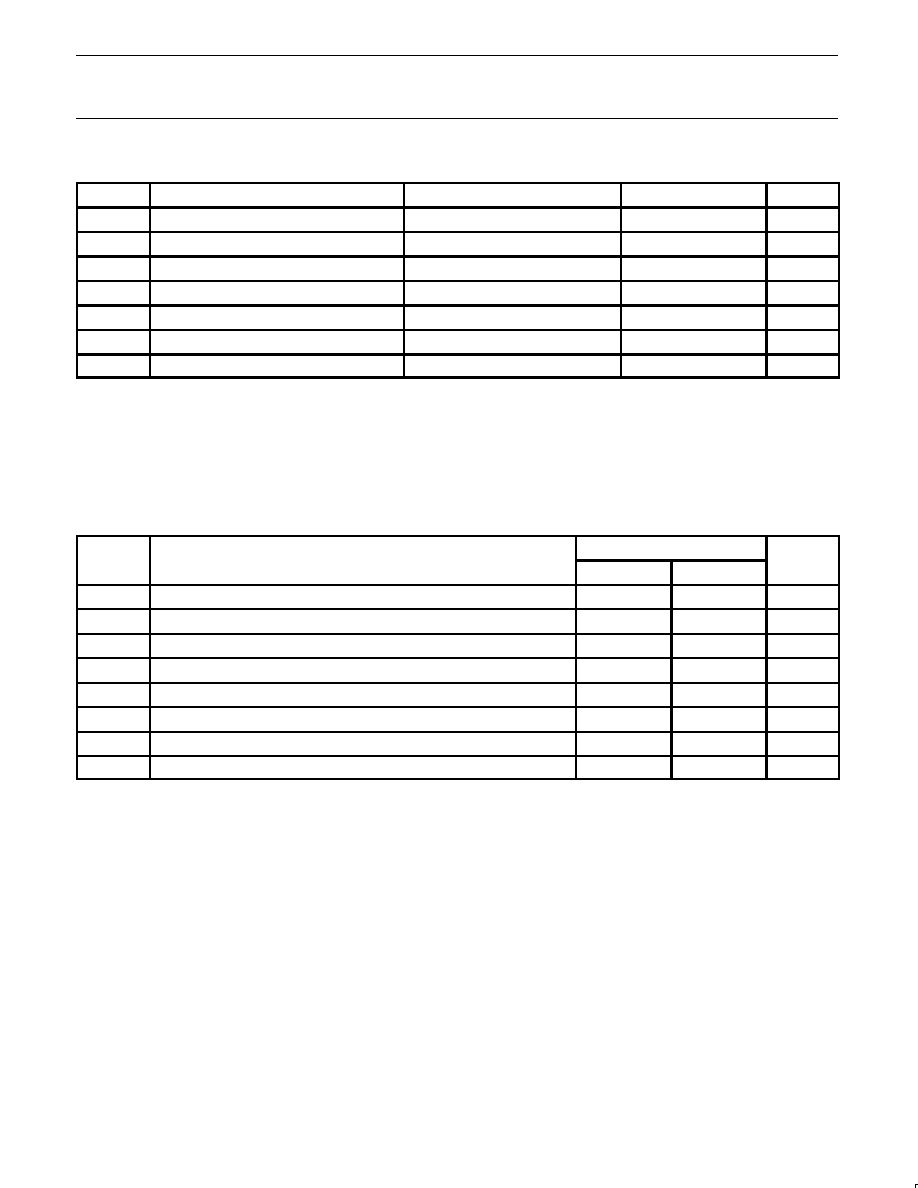
FUNCTION TABLE for Register nAx or nBx
INPUTS
INTERNAL
OPERATING
nAx or nBx
nCPXX
nCEXX
Q
MODE
X
X
H
NC
Hold data
L
H
L
L
L
H
Load data
H = High voltage level
L
= Low voltage level
= Low-to-High transition
X = Don't care
XX = AB or BA
NC= No change
Philips Semiconductors Advanced BiCMOS Products
Product specification
MB2052
Dual octal registered transceiver (3-State)
August 23, 1993
3
FUNCTION TABLE for Output Enable
INPUTS
INTERNAL
nAx or nBx
OPERATING
nOEXX
Q
OUTPUTS
MODE
H
X
Z
Disable outputs
L
L
L
H
L
H
Enable outputs
H = High voltage level
L
= Low voltage level
X = Don't care
XX = AB or BA
Z = High impedance "off" state
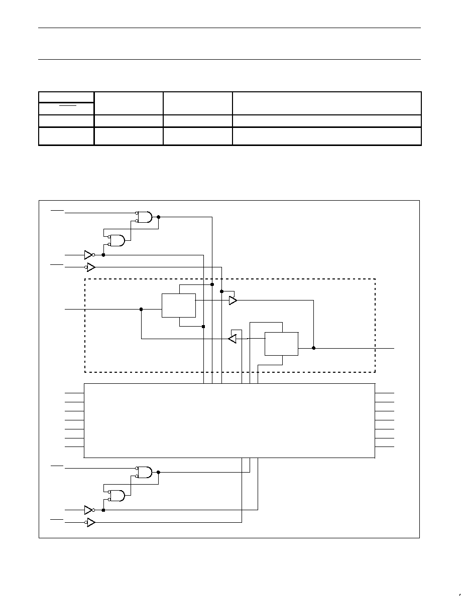
LOGIC DIAGRAM
nCEAB
CE
Q
CP
D
CE
Q
CP
D
DETAIL A
DETAIL A X 7
nCPAB
nOEAB
nA0
nA2
nCPBA
nOEBA
nB0
nA3
nA4
nA5
nA6
nA7
nCEBA
nB1
nB2
nB3
nB4
nB5
nB6
nB7
nA1
Philips Semiconductors Advanced BiCMOS Products
Product specification
MB2052
Dual octal registered transceiver (3-State)
August 23, 1993
4
ABSOLUTE MAXIMUM RATINGS
1, 2
SYMBOL
PARAMETER
CONDITIONS
RATING
UNIT
V
CC
DC supply voltage
0.5 to +7.0
V
I
IK
DC input diode current
V
I
< 0
18
mA
V
I
DC input voltage
3
1.2 to +7.0
V
I
OK
DC output diode current
V
O
< 0
50
mA
V
OUT
DC output voltage
3
output in Off or High state
0.5 to +5.5
V
I
OUT
DC output current
output in Low state
128
mA
T
stg
Storage temperature range
65 to 150
°
C
NOTES:
1. Stresses beyond those listed may cause permanent damage to the device. These are stress ratings only and functional operation of the
device at these or any other conditions beyond those indicated under "recommended operating conditions" is not implied. Exposure to
absolute-maximum-rated conditions for extended periods may affect device reliability.
2. The performance capability of a high-performance integrated circuit in conjunction with its thermal environment can create junction
temperatures which are detrimental to reliability. The maximum junction temperature of this integrated circuit should not exceed 150
°
C.
3. The input and output voltage ratings may be exceeded if the input and output current ratings are observed.
RECOMMENDED OPERATING CONDITIONS
SYMBOL
PARAMETER
LIMITS
UNIT
MIN
MAX
V
CC
DC supply voltage
4.5
5.5
V
V
I
Input voltage
0
V
CC
V
V
IH
High-level input voltage
2.0
V
V
IL
Low-level Input voltage
0.8
V
I
OH
High-level output current
32
mA
I
OL
Low-level output current
64
mA
t/
v
Input transition rise or fall rate
0
10
ns/V
T
amb
Operating free-air temperature range
40
+85
°
C
Philips Semiconductors Advanced BiCMOS Products
Product specification
MB2052
Dual octal registered transceiver (3-State)
August 23, 1993
5
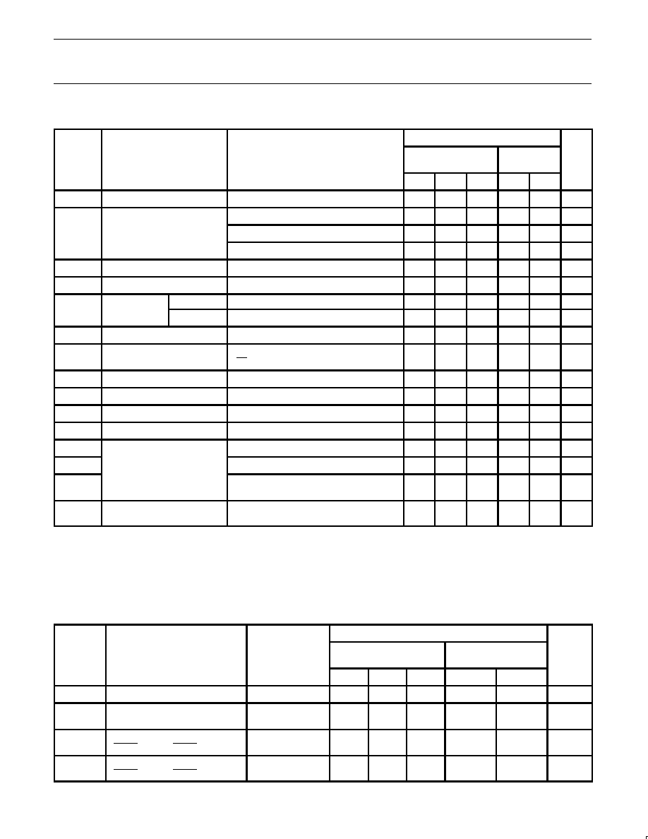
DC ELECTRICAL CHARACTERISTICS
LIMITS
SYMBOL
PARAMETER
TEST CONDITIONS
T
amb
= +25
°
C
T
amb
= 40
°
C
to +85
°
C
UNIT
MIN
TYP
MAX
MIN
MAX
V
IK
Input clamp voltage
V
CC
= 4.5V; I
IK
= 18mA
0.9
1.2
1.2
V
V
CC
= 4.5V; I
OH
= 3mA; V
I
= V
IL
or V
IH
2.5
2.9
2.5
V
V
OH
High-level output voltage
V
CC
= 5.0V; I
OH
= 3mA; V
I
= V
IL
or V
IH
3.0
3.4
3.0
V
V
CC
= 4.5V; I
OH
= 32mA; V
I
= V
IL
or V
IH
2.0
2.4
2.0
V
V
OL
Low-level output voltage
V
CC
= 4.5V; I
OL
= 64mA; V
I
= V
IL
or V
IH
0.42
0.55
0.55
V
V
RST
Power-up output low voltage
3
V
CC
= 5.5V; I
OL
= 1mA; V
I
= GND or V
CC
0.13
0.55
0.55
V
I
I
Input leakage
Control pins
V
CC
= 5.5V; V
I
= GND or 5.5V
±
0.01
±
1.0
±
1.0
µ
A
current
Data pins
V
CC
= 5.5V; V
I
= GND or 5.5V
5
100
100
µ
A
I
OFF
Power-off leakage current
V
CC
= 0V; V
O
or V
I
4.5V
±
5.0
±
100
±
100
µ
A
I
PU/PD
Power-up/down 3-State
output current
4
V
CC
= 2.1V; V
O
= 0.5V; V
I
= GND or V
CC
;
V
OE
= Don't care
±
5.0
±
50
±
50
µ
A
I
IH
+ I
OZH
3-State output High current
V
CC
= 5.5V; V
O
= 2.7V; V
I
= V
IL
or V
IH
5.0
50
50
µ
A
I
IL
+ I
OZL
3-State output Low current
V
CC
= 5.5V; V
O
= 0.5V; V
I
= V
IL
or V
IH
5.0
50
50
µ
A
I
CEX
Output High leakage current
V
CC
= 5.5V; V
O
= 5.5V; V
I
= GND or V
cc
5.0
50
50
µ
A
I
O
Output current
1
V
CC
= 5.5V; V
O
= 2.5V
50
70
180
50
180
mA
I
CCH
V
CC
= 5.5V; Outputs High, V
I
= GND or V
CC
120
250
250
µ
A
I
CCL
Quiescent supply current
V
CC
= 5.5V; Outputs Low, V
I
= GND or V
CC
39
60
60
mA
I
CCZ
V
CC
= 5.5V; Outputs 3-State;
V
I
= GND or V
CC
120
250
250
µ
A
I
CC
Additional supply current per
input pin
2
V
CC
= 5.5V; one input at 3.4V,
other inputs at V
CC
or GND
0.5
1.5
1.5
mA
NOTES:
1. Not more than one output should be tested at a time, and the duration of the test should not exceed one second.
2. This is the increase in supply current for each input at 3.4V.
3. For valid test results, data must not be loaded into the flip-flops (or latches) after applying the power.
4. This parameter is valid for any V
CC
between 0V and 2.1V with a transition time of up to 10msec. From V
CC
= 2.1V to V
CC
= 5V
±
10% a
transition time of up to 100
µ
sec is permitted.
AC CHARACTERISTICS
GND = 0V; t
R
= t
F
= 2.5ns; C
L
= 50pF, R
L
= 500
LIMITS
SYMBOL
PARAMETER
WAVEFORM
T
amb
= +25
°
C
V
CC
= +5.0V
T
amb
= 40
°
C to +85
°
C
V
CC
= +5.0V
±
0.5V
UNIT
MIN
TYP
MAX
MIN
MAX
f
MAX
Maximum clock frequency
1
200
250
200
MHz
t
PLH
t
PHL
Propagation delay
nCPBA to nAx, nCPAB to nBx
1
2.1
2.6
3.7
4.1
4.9
5.3
2.1
2.6
5.4
5.8
ns
t
PZH
t
PZL
Output enable time
nOEBA to nAx, nOEAB to nBx
3
4
1.2
2.0
2.9
3.7
4.1
5.0
1.2
2.0
4.8
5.8
ns
t
PHZ
t
PLZ
Output disable time
nOEBA to nAx, nOEAB to nBx
3
4
1.0
1.5
3.5
3.0
4.7
4.1
1.0
1.5
5.2
4.6
ns